 | –≠–ª–µ–∫—Ç—Ä–æ–Ω–Ω—ã–π –∫–æ–º–ø–æ–Ω–µ–Ω—Ç: HIP6301 | –°–∫–∞—á–∞—Ç—å:  PDF PDF  ZIP ZIP |

1
File Number
4765.1
HIP6301
Microprocessor CORE Voltage Regulator
Multi-Phase Buck PWM Controller
The HIP6301 multi-phase PWM control IC together with its
companion gate drivers, the HIP6601, HIP6602 or HIP6603
and internal MOSFETs provides a precision voltage
regulation system for advanced microprocessors.
Multiphase power conversion is a marked departure from
earlier single phase converter configurations previously
employed to satisfy the ever increasing current demands of
modern microprocessors. Multi-phase convertors, by
distributing the power and load current results in smaller and
lower cost transistors with fewer input and output capacitors.
These reductions accrue from the higher effective
conversion frequency with higher frequency ripple current
due to the phase interleaving process of this topology. For
example, a three phase convertor operating at 350kHz will
have a ripple frequency of 1.05MHz. Moreover, greater
convertor bandwidth of this design results in faster response
to load transients.
Outstanding features of this controller IC include
programmable VID codes from the microprocessor that
range from 1.100V to 1.850V with a system accuracy of
±
1%. Pull up currents on these VID pins eliminates the need
for external pull up resistors. In addition "droop"
compensation, used to reduce the overshoot or undershoot
of the CORE voltage, is easily programmed with a single
resistor.
Another feature of this controller IC is the PGOOD monitor
circuit which is held low until the CORE voltage increases,
during its Soft-Start sequence, to within 10% of the
programmed voltage. Over-voltage, 15% above programmed
CORE voltage, results in the converter shutting down and
turning the lower MOSFETs ON to clamp and protect the
microprocessor. Under voltage is also detected and results
in PGOOD low if the CORE voltage falls 10% below the
programmed level. Over-current protection reduces the
regulator current to less than 25% of the programmed trip
value. These features provide monitoring and protection for
the microprocessor and power system.
Features
∑ Multi-Phase Power Conversion
∑ Precision Channel Current Sharing
- Loss Less Current Sampling - Uses r
DS(ON)
∑ Precision CORE Voltage Regulation
-
±
1% System Accuracy Over Temperature
∑ Microprocessor Voltage Identification Input
- 5-Bit VID Input
- 1.100V to 1.850V in 25mV Steps
- Programmable "Droop" Voltage
∑ Fast Transient Recovery Time
∑ Over Current Protection
∑ Automatic Selection of 2, 3, or 4 Phase Operation
∑ High Ripple Frequency, (Channel Frequency) Times
Number Channels . . . . . . . . . . . . . . . . . 100kHz to 6MHz
Pinout
HIP6301 (SOIC)
TOP VIEW
Ordering Information
PART NUMBER
TEMP. (
o
C)
PACKAGE
PKG. NO.
HIP6301CB
0 to 70
20 Ld SOIC
M20.3
HIP6301CB-T
20 Ld SOIC Tape and Reel
HIP6301EVAL1
Evaluation Platform
11
12
13
14
15
16
17
18
20
19
10
9
8
7
6
5
4
3
2
1
VID4
VID3
VID2
VID1
VID0
FS/DIS
PWM2
PGOOD
PWM3
ISEN4
ISEN1
V
CC
GND
ISEN3
FB
PWM4
VSEN
COMP
PWM1
ISEN2
Data Sheet
March 2000
CAUTION: These devices are sensitive to electrostatic discharge; follow proper IC Handling Procedures.
1-888-INTERSIL or 321-724-7143
|
Copyright
©
Intersil Corporation 2000

2
Block Diagram
D/A
CURRENT
CORRECTION
OV
LATCH
POWER-ON
RESET (POR)
SOFT-
START
AND FAULT
LOGIC
CHANNEL
DETECTOR
+
-
+
-
UV
OVP
+
-
E/A
+
-
PWM
PWM
OC
+
-
PWM1
PWM2
PWM3
PWM4
GND
PGOOD
V
CC
FB
I_TRIP
FS/EN
S
STATE
I_TOT
+
-
+
-
+
-
+
-
+
+
+
+
+
-
PHASE
+
-
PWM
+
-
PWM
CLOCK AND
NUMBER
THREE
VID0
VID1
VID2
VID3
COMP
VSEN
GENERATOR
SAWTOOTH
X1.15
X 0.9
ISEN1
ISEN2
ISEN3
ISEN4
VID4
HIP6301

3
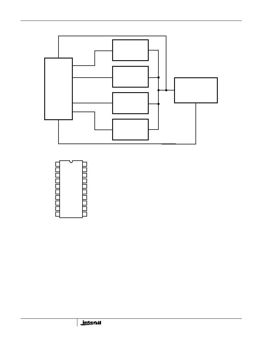
Simplified Power System Diagram
Functional Pin Description
VID4 (Pin 1), VID3(Pin 2), VID2 (Pin 3), VID1(Pin 4)
and VID0 (Pin 5)
Voltage Identification inputs from microprocessor. These pins
respond to TTL and 3.3V logic signals. The HIP6301 decodes
VID bits to establish the output voltage. See Table 1.
COMP (Pin 6)
Output of the internal error amplifier. Connect this pin to the
external feedback and compensation network.
FB (Pin 7)
Inverting input of the internal error amplifier.
FS/DIS (Pin 8)
Channel frequency, F
SW
, select and disable. A resistor from
this pin to ground sets the switching frequency of the
converter. Pulling this pin to ground disables the converter
and three states the PWM outputs. See Figure 10.
GND (Pin 9)
Bias and reference ground. All signals are referenced to this
pin.
VSEN (Pin 10)
Power good monitor input. Connect to the microprocessor-
CORE voltage.
PWM1 (Pin 15), PWM2 (Pin 14), PWM3 (Pin 11) and
PWM4 (Pin 18)
PWM outputs for each driven channel in use. Connect these
pins to the PWM input of a HIP6601/2/3 driver. For systems
which use 3 channels, connect PWM4 high. Two channel
systems connect PWM3 and PWM4 high.
ISEN1 (Pin 16), ISEN2 (Pin 13), ISEN3 (Pin 12) and
ISEN4 (Pin 17)
Current sense inputs from the individual converter channel's
phase nodes. Unused sense lines MUST be left open.
PGOOD (Pin 19)
Power good. This pin provides a logic-high signal when the
microprocessor CORE voltage (VSEN pin) is within specified
limits and Soft-Start has timed out.
V
CC
(Pin 20)
Bias supply. Connect this pin to a 5V supply.
SYNCHRONOUS
HIP6301
MICROPROCESSOR
VSEN
VID
RECTIFIED BUCK
CHANNEL
SYNCHRONOUS
RECTIFIED BUCK
CHANNEL
SYNCHRONOUS
RECTIFIED BUCK
CHANNEL
SYNCHRONOUS
RECTIFIED BUCK
CHANNEL
PWM 1
PWM 2
PWM 3
PWM 4
11
12
13
14
15
16
17
18
20
19
10
9
8
7
6
5
4
3
2
1
VID4
VID3
VID2
VID1
VID0
FS/DIS
PWM2
PGOOD
PWM3
ISEN4
ISEN1
V
CC
GND
ISEN3
FB
PWM4
VSEN
COMP
PWM1
ISEN2
HIP6301
HIP6301

4
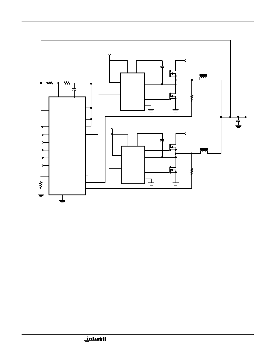
Typical Application - 2 Phase Converter Using HIP6601 Gate Drivers
MAIN
CONTROL
HIP6301
VID3
VID0
PGOOD
FB
+5V
COMP
PWM3
PWM2
PWM1
ISEN3
ISEN2
ISEN1
VSEN
DRIVER
HIP6601
PWM
VCC
BOOT
UGATE
PHASE
LGATE
V
IN
= +5V
PVCC
PWM
VCC
BOOT
UGATE
PHASE
LGATE
V
IN
= +5V
DRIVER
HIP6601
PVCC
FS/DIS
PWM4
ISEN4
NC
GND
GND
GND
V
CC
+V
CORE
NC
+12V
+12V
VID2
VID4
VID1
HIP6301

5
HIP6301
Typical Application - 4 Phase Converter Using HIP6602 Gate Drivers
VID3
VID2
VID1
VID0
FB
+5V
COMP
PWM1
PWM2
ISEN2
PWM3
PWM4
ISEN4
VSEN
FS/DIS
ISEN1
ISEN3
GND
V
IN
+12V
BOOT2
UGATE2
PHASE2
LGATE2
BOOT1
UGATE1
PHASE1
LGATE1
PWM1
PVCC
+5V
V
CC
V
IN
= +12V
+12V
DUAL
DRIVER
HIP6602
V
IN
+12V
BOOT4
UGATE4
PHASE4
LGATE4
BOOT3
UGATE3
PHASE3
LGATE3
PWM3
PVCC
+5V
V
CC
V
IN
+12V
+12V
DUAL
DRIVER
HIP6602
PGOOD
GND
GND
V
CC
+V
CORE
L
01
L
02
L
03
L
04
PWM2
PWM4
MAIN
CONTROL
HIP6301
VID4

6
Absolute Maximum Ratings
Supply Voltage, V
CC
. . . . . . . . . . . . . . . . . . . . . . . . . . . . . . . . . +7V
Input, Output, or I/O Voltage . . . . . . . . . . GND -0.3V to V
CC
+ 0.3V
ESD Classification . . . . . . . . . . . . . . . . . . . . . . . . . . . . . . . . . . 1.5KV
Recommended Operating Conditions
Supply Voltage . . . . . . . . . . . . . . . . . . . . . . . . . . . . . . . . . . +5V
±
5%
Ambient Temperature. . . . . . . . . . . . . . . . . . . . . . . . . . . 0
o
C to 70
o
C
Thermal Information
Thermal Resistance (Typical, Note 1)
JA
(
o
C/W)
SOIC Package . . . . . . . . . . . . . . . . . . . . . . . . . . . . .
87
Maximum Junction Temperature . . . . . . . . . . . . . . . . . . . . . . .150
o
C
Maximum Storage Temperature Range . . . . . . . . . . -65
o
C to 150
o
C
Maximum Lead Temperature (Soldering 10s) . . . . . . . . . . . . .300
o
C
(SOIC - Lead Tips Only)
CAUTION: Stress above those listed in "Absolute Maximum Ratings" may cause permanent damage to the device. This is a stress only rating and operation of the
device at these or any other conditions above those indicated in the operational section of this specification is not implied.
NOTE:
1.
JA
is measured with the component mounted on a low effective thermal conductivity test board in free air. (See Tech Brief TB379 for details.)
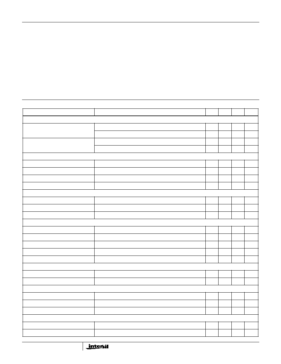
Electrical Specifications
Operating Conditions: V
CC
= 5V, T
A
= 0
o
C to 70
o
C, Unless Otherwise Specified
PARAMETER
TEST CONDITIONS
MIN
TYP
MAX
UNITS
INPUT SUPPLY POWER
Input Supply Current
R
T
= 100k
-
10
15
mA
EN = 0V
4.25
8.8
4.5
mA
POR (Power-On Reset) Threshold
V
CC
Rising
4.25
4.38
4.5
V
V
CC
Falling
3.75
3.88
4.00
V
REFERENCE AND DAC
System Accuracy
Percent system deviation from programmed VID Codes
-1
-
1
%
DAC (VID0 - VID3) Input Low Voltage
DAC Programming Input Low Threshold Voltage
-
-
0.8
V
DAC (VID0 - VID3) Input High Voltage
DAC Programming Input High Threshold Voltage
2.0
-
-
V
VID Pull-Up
VIDx = 0V or VIDx = 3V
10
20
40
µ
A
CHANNEL GENERATOR
Frequency, F
SW
R
T
= 100k
,
±
1%
224
280
336
kHz
Adjustment Range
See Figure 10
0.05
-
1.5
MHz
Disable Voltage
Maximum voltage at FS/DIS to disable controller. I
FS/DIS
= 1mA.
-
1.2
1.0
V
ERROR AMPLIFIER
DC Gain
R
L
= 10K to ground
-
72
-
dB
Gain-Bandwidth Product
C
L
= 100pF, R
L
= 10K to ground
-
18
-
MHz
Slew Rate
C
L
= 100pF, R
L
= 10K to ground
-
5.3
-
V/
µ
s
Maximum Output Voltage
R
L
= 10K to ground
3.6
4.1
-
V
Minimum Output Voltage
R
L
= 10K to ground
-
0.16
0.5
V
I
SEN
Full Scale Input Current
-
50
-
µ
A
Over-Current Trip Level
-
82.5
-
µ
A
POWER GOOD MONITOR
Under-Voltage Threshold
VSEN Rising
-
0.92
-
V
DAC
Under-Voltage Threshold
VSEN Falling
-
0.90
-
V
DAC
PGOOD Low Output Voltage
I
PGOOD
= 4mA
-
0.18
0.4
V
PROTECTION
Over-Voltage Threshold
VSEN Rising
1.12
1.15
1.2
V
DAC
Percent Over-Voltage Hysteresis
VSEN Falling after Over-Voltage
-
2
-
%
HIP6301

7
Operation
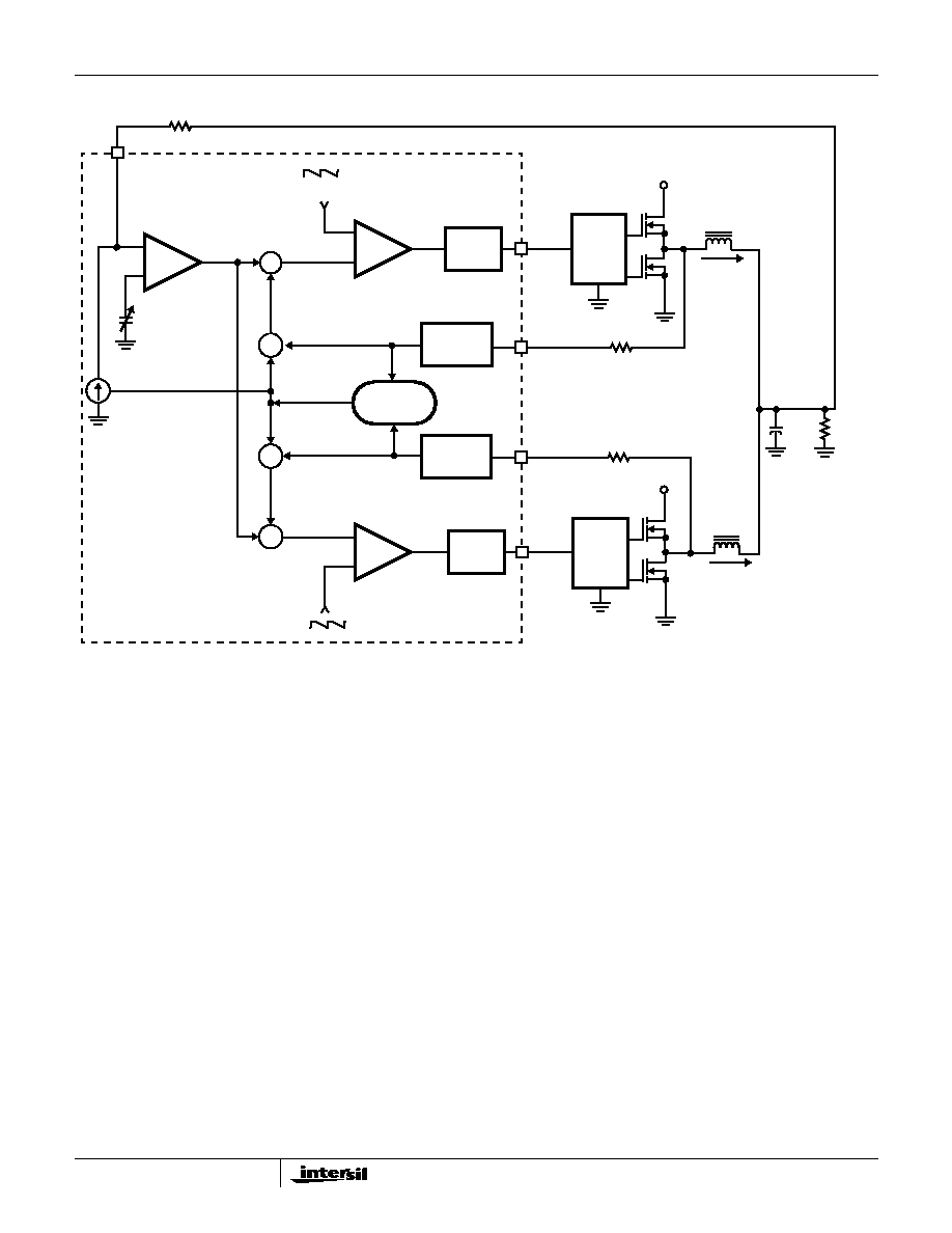
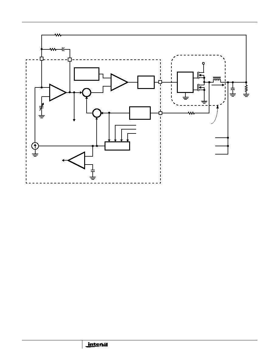
Figure 1 shows a simplified diagram of the voltage regulation
and current control loops. Both voltage and current feedback
are used to precisely regulate voltage and tightly control
output currents, I
L1
and I
L2
, of the two power channels. The
voltage loop comprises the Error Amplifier, Comparators,
gate drivers and output MOSFETs. The Error Amplifier is
essentially connected as a voltage follower that has as an
input, the Programmable Reference DAC and an output that
is the CORE voltage.
Voltage Loop
Feedback from the CORE voltage is applied via resistor R
IN
to the inverting input of the Error Amplifier. This signal can
drive the Error Amplifier output either high or low, depending
upon the CORE voltage. Low CORE voltage makes the
amplifier output move towards a higher output voltage level.
Amplifier output voltage is applied to the positive inputs of
the Comparators via the Correction summing networks. Out-
of-phase sawtooth signals are applied to the two
Comparators inverting inputs. Increasing Error Amplifier
voltage results in increased Comparator output duty cycle.
This increased duty cycle signal is passed through the PWM
CIRCUIT with no phase reversal and on to the HIP6601,
again with no phase reversal for gate drive to the upper
MOSFETs, Q1 and Q3. Increased duty cycle or ON time for
the MOSFET transistors results in increased output voltage
to compensate for the low output voltage sensed.
Current Loop
The current control loop works in a similar fashion to the
voltage control loop, but with current control information
applied individually to each channel's Comparator. The
information used for this control is the voltage that is
developed across r
DS(ON)
of each lower MOSFET, Q2 and
Q4, when they are conducting. A single resistor converts
and scales the voltage across the MOSFETs to a current
that is applied to the Current Sensing circuit within the
HIP6301. Output from these sensing circuits is applied to the
current averaging circuit. Each PWM channel receives the
difference current signal from the summing circuit that
compares the average sensed current to the individual
channel current. When a power channel's current is greater
CURRENT
SENSING
COMPARATOR
PWM
CIRCUIT
+
R
ISEN1
+
CORRECTION
ERROR
AMPLIFIER
FB
REFERENCE
I
SEN1
R
IN
V
CORE
Q3
Q4
L
02
PHASE
PWM1
I
L2
DAC
HIP6303
C
OUT
R
LOAD
V
IN
HIP6601
-
Q1
Q2
L
01
PHASE
I
L1
V
IN
HIP6601
CURRENT
SENSING
COMPARATOR
PWM
CIRCUIT
CORRECTION
PWM2
-
I AVERAGE
+
+
+
-
PROGRAMMABLE
R
ISEN2
I
SEN2
-
-
-
-
+
+
CURRENT
AVERAGING
FIGURE 1. SIMPLIFIED BLOCK DIAGRAM OF THE HIP6301 VOLTAGE AND CURRENT CONTROL LOOPS FOR A TWO POWER
CHANNEL REGULATOR
HIP6301
HIP6301

8
than the average current, the signal applied via the summing
Correction circuit to the Comparator, reduces the output
pulse width of the Comparator to compensate for the
detected "above average" current in that channel.
Droop Compensation
In addition to control of each power channel's output current,
the average channel current is also used to provide CORE
voltage "droop" compensation. Average full channel current
is defined as 50
µ
A. By selecting an input resistor, R
IN
, the
amount of voltage droop required at full load current can be
programmed. The average current driven into the FB pin
results in a voltage increase across resistor R
IN
that is in the
direction to make the Error Amplifier "see" a higher voltage
at the inverting input, resulting in the Error Amplifier adjust-
ing the output voltage lower. The voltage developed across
R
IN
is equal to the "droop" voltage. See the "Current Sensing
and Balancing" section for more details.
Applications and Convertor Start-Up
Each PWM power channel's current is regulated. This
enables the PWM channels to accurately share the load
current for enhanced reliability. The HIP6601, HIP6602 or
HIP6603 MOSFET driver interfaces with the HIP6301. For
more information, see the HIP6601, HIP6602 or HIP6603
data sheets.
The HIP6301 is capable of controlling up to 4 PWM power
channels. Connecting unused PWM outputs to V
CC
automatically sets the number of channels. The phase
relationship between the channels is 360
o
/number of active
PWM channels. For example, for three channel operation,
the PWM outputs are separated by 120
o
. Figure 2 shows the
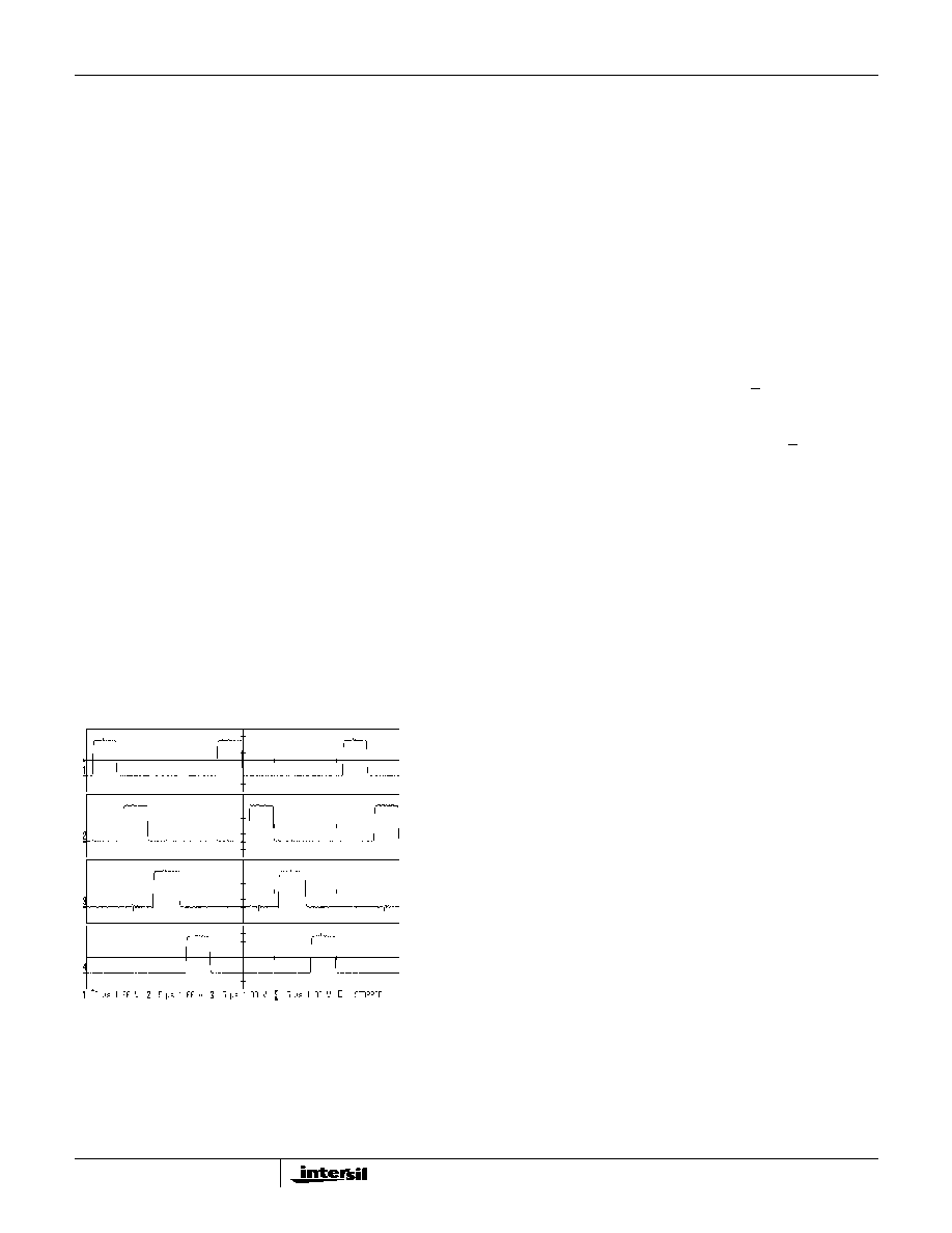
PWM output signals for a four channel system.
Power supply ripple frequency is determined by the channel
frequency, F
SW
, multiplied by the number of active channels.
For example, if the channel frequency is set to 250kHz and
there are three phases, the ripple frequency is 750kHz.
The IC monitors and precisely regulates the CORE voltage
of a microprocessor. After initial start-up, the controller also
provides protection for the load and the power supply. The
following section discusses these features.
Initialization
The HIP6301 usually operates from an ATX power supply.
Many functions are initiated by the rising supply voltage to
the V
CC
pin of the HIP6301. Oscillator, Sawtooth Generator,
Soft-Start and other functions are initialized during this
interval. These circuits are controlled by POR, Power-On
Reset. During this interval, the PWM outputs are driven to a
three state condition that makes these outputs essentially
open. This state results in no gate drive to the output
MOSFETS.
Once the V
CC
voltage reaches 4.375V (+125mV), a voltage
level to insure proper internal function, the PWM outputs are
enabled and the Soft-Start sequence is initiated. If for any
reason, the V
CC
voltage drops below 3.875V (+125mV). the
POR circuit shuts the converter down and again three states
the PWM outputs.
Soft-Start
After the POR function is completed with V
CC
reaching
4.375V, the Soft-Start sequence is initiated. Soft-Start, by its
slow rise in CORE voltage from zero, avoids an over-current
condition by slowly charging the discharged output
capacitors. This voltage rise is initiated by an internal DAC
that slowly raises the reference voltage to the error amplifier
input. The voltage rise is controlled by the oscillator
frequency and the DAC within the HIP6301, therefore, the
output voltage is effectively regulated as it rises to the final
programmed CORE voltage value.
For the first 32 PWM switching cycles, the DAC output
remains inhibited and the PWM outputs remain three stated.
From the 33rd cycle and for another, approximately 150
cycles the PWM output remains low, clamping the lower
output MOSFETs to ground, see Figure 3. The time
variability is due to the Error Amplifier, Sawtooth Generator
and Comparators moving into their active regions. After this
short interval, the PWM outputs are enabled and increment
the PWM pulse width from zero duty cycle to operational
pulse width, thus allowing the output voltage to slowly reach
the CORE voltage. The CORE voltage will reach its
programmed value before the 2048 cycles, but the PGOOD
output will not be initiated until the 2048th PWM switching
cycle.
The Soft-Start time or delay time, DT = 2048/F
SW
. For an
oscillator frequency, F
SW
, of 200kHz, the first 32 cycles or
160
µ
s, the PWM outputs are held in a three state level as
explained above. After this period and a short interval
described above, the PWM outputs are initiated and the
voltage rises in 10.08ms, for a total delay time DT of
10.24ms.
PWM 1
PWM 2
PWM 3
PWM 4
FIGURE 2. FOUR PHASE PWM OUTPUT AT 500kHz
HIP6301
HIP6301

9
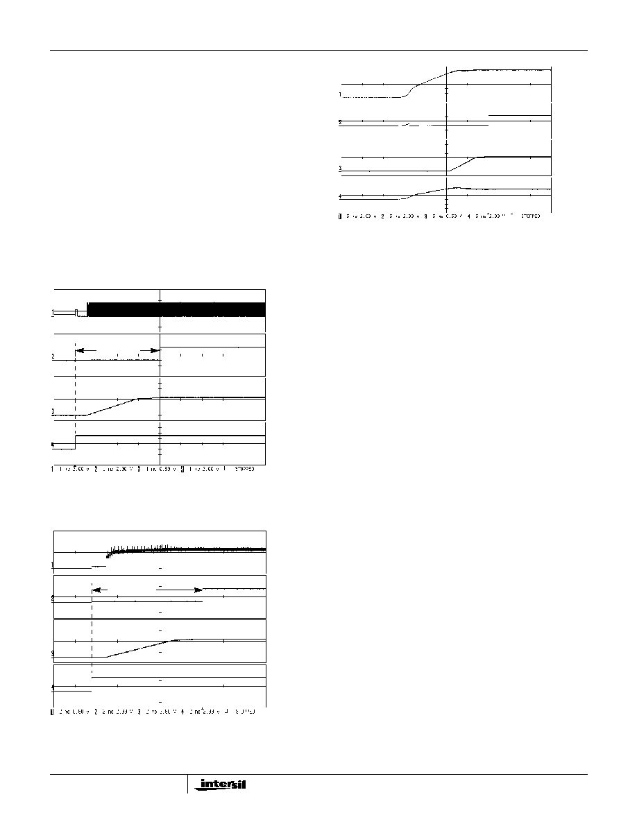
Figure 3 shows the start-up sequence as initiated by a fast
rising 5V supply, V
CC,
applied to the HIP6301. Note the
short rise to the three state level in PWM 1 output during first
32 PWM cycles.
Figure 4 shows the waveforms when the regulator is
operating at 200kHz. Note that the Soft-Start duration is a
function of the Channel Frequency as explained previously.
Also note the pulses on the COMP terminal. These pulses
are the current correction signal feeding into the comparator
input (see the Block Diagram on page 2).
Figure 5 shows the regulator operating from an ATX supply.
In this figure, note the slight rise in PGOOD as the 5V supply
rises.The PGOOD output stage is made up of NMOS and
PMOS transistors. On the rising V
CC
, the PMOS device
becomes active slightly before the NMOS transistor pulls
"down", generating the slight rise in the PGOOD voltage.
Note that Figure 5 shows the 12V gate driver voltage
available before the 5V supply to the HIP6301 has reached
its threshold level. If conditions were reversed and the 5V
supply was to rise first, the start-up sequence would be
different. In this case the HIP6303 will sense an over-current
condition due to charging the output capacitors. The supply
will then restart and go through the normal Soft-Start cycle.
Fault Protection
The HIP6301 protects the microprocessor and the entire
power system from damaging stress levels. Within the
HIP6301 both Over-Voltage and Over-Current circuits are
incorporated to protect the load and regulator.
Over-Voltage
The VSEN pin is connected to the microprocessor CORE
voltage. A CORE over-voltage condition is detected when
the VSEN pin goes more than 15% above the programmed
VID level.
The over-voltage condition is latched, disabling normal PWM
operation, and causing PGOOD to go low. The latch can
only be reset by lowering and returning V
CC
high to initiate a
POR and Soft-Start sequence.
During a latched over-voltage, the PWM outputs will be
driven either low or three state, depending upon the VSEN
input. PWM outputs are driven low when the VSEN pin
detects that the CORE voltage is 15% above the
programmed VID level. This condition drives the PWM
outputs low, resulting in the lower or synchronous rectifier
MOSFETS to conduct and shunt the CORE voltage to
ground to protect the load.
If after this event, the CORE voltage falls below the over-
voltage limit (plus some hysteresis), the PWM outputs will
three state. The HIP6601 family drivers pass the three state
information along, and shuts off both upper and lower
MOSFETs. This prevents "dumping" of the output capacitors
back through the lower MOSFETs, avoiding a possibly
PWM 1
PGOOD
V
CORE
5V
OUTPUT
V
CC
V
IN
= 12V
DELAY TIME
FIGURE 3. START-UP OF 4 PHASE SYSTEM OPERATING AT
500kHz
PGOOD
V
CORE
5V
V COMP
V
CC
V
IN
= 12V
DELAY TIME
FIGURE 4. START-UP OF 4 PHASE SYSTEM OPERATING AT
200kHz
12V ATX
SUPPLY
PGOOD
5 V ATX
V
CORE
SUPPLY
ATX SUPPLY ACTIVATED BY ATX "PS-ON PIN"
V
IN
= 5V, CORE LOAD CURRENT = 31A
FIGURE 5. SUPPLY POWERED BY ATX SUPPLY
FREQUENCY 200kHz
HIP6301
HIP6301

10
destructive ringing of the capacitors and output inductors. If
the conditions that caused the over-voltage still persist, the
PWM outputs will be cycled between three state and V
CORE
clamped to ground, as a hysteretic shunt regulator.
Under-Voltage
The VSEN pin also detects when the CORE voltage falls
more than 10% below the VID programmed level. This
causes PGOOD to go low, but has no other effect on
operation and is not latched. There is also hysteresis in this
detection point.
Over-Current
In the event of an over-current condition, the over-current
protection circuit reduces the average current delivered to
less than 25% of the current limit. When an over-current
condition is detected, the controller forces all PWM outputs
into a three state mode. This condition results in the gate
driver removing drive to the output stages.The HIP6301
goes into a wait delay timing cycle that is equal to the Soft-
Start ramp time. PGOOD also goes "low" during this time
due to VSEN going below its threshold voltage.To lower the
average output dissipation, the Soft-Start initial wait time is
increased from 32 to 2048 cycles, then the Soft-Start ramp is
initiated. At a PWM frequency of 200kHz, for instance, an
over-current detection would cause a dead time of 10.24ms,
then a ramp of 10.08ms.
At the end of the delay, PWM outputs are restarted and the
soft start ramp is initiated. If a short is present at that time,
the cycle is repeated. This is the hiccup mode.
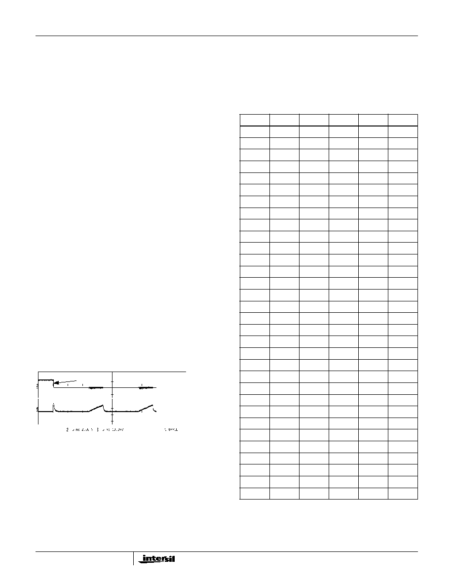
Figure 6 shows the supply shorted under operation and the
hiccup operating mode described above. Note that due to
the high short circuit current, over-current is detected before
completion of the start-up sequence so the delay is not quite
as long as the normal Soft-Start cycle.
CORE Voltage Programming
The voltage identification pins (VID0, VID1, VID3, and VID4)
set the CORE output voltage. Each VID pin is pulled to V
CC
by an internal 20
µ
A current source and accepts open-
collector/open-drain/open-switch-to-ground or standard low-
voltage TTL or CMOS signals.
Table 1 shows the nominal DAC voltage as a function of the
VID codes. The power supply system is
±
1% accurate over
the operating temperature and voltage range.
PGOOD
SHORT
50A/Div
CURRENT
ATX SUPPLY ACTIVATED BY ATX "PS-ON PIN"
SUPPLY FREQUENCY = 200kHz, V
IN
= 12V
HICCUP MODE. SUPPLY POWERED BY ATX SUPPLY
CORE LOAD CURRENT = 31A, 5V LOAD = 5A
SHORT APPLIED HERE
FIGURE 6. SHORT APPLIED TO SUPPLY AFTER POWER-UP
TABLE 1. VOLTAGE IDENTIFICATION CODES
VID4
VID3
VID2
VID1
VID0
VDAC
1
1
1
1
1
Off
1
1
1
1
0
1.100
1
1
1
0
1
1.125
1
1
1
0
0
1.150
1
1
0
1
1
1.175
1
1
0
1
0
1.200
1
1
0
0
1
1.225
1
1
0
0
0
1.250
1
0
1
1
1
1.275
1
0
1
1
0
1.300
1
0
1
0
1
1.325
1
0
1
0
0
1.350
1
0
0
1
1
1.375
1
0
0
1
0
1.400
1
0
0
0
1
1.425
1
0
0
0
0
1.450
0
1
1
1
1
1.475
0
1
1
1
0
1.500
0
1
1
0
1
1.525
0
1
1
0
0
1.550
0
1
0
1
1
1.575
0
1
0
1
0
1.600
0
1
0
0
1
1.625
0
1
0
0
0
1.650
0
0
1
1
1
1.675
0
0
1
1
0
1.700
0
0
1
0
1
1.725
0
0
1
0
0
1.750
0
0
0
1
1
1.775
0
0
0
1
0
1.800
0
0
0
0
1
1.825
0
0
0
0
0
1.850
HIP6301
HIP6301

11
Current Sensing and Balancing
Overview
The HIP6301 samples the on-state voltage drop across each
synchronous rectifier FET, Q2, as an indication of the
inductor current in that phase, see Figure 7. Neglecting AC
effects (to be discussed later), the voltage drop across Q2 is
simply r
DS(ON)
(Q2) x inductor current (I
L
). Note that I
L
, the
inductor current, is either 1/2, 1/3, or 1/4 of the total current
(I
LT
), depending on how many phases are in use.
The voltage at Q2's drain, the PHASE node, is applied to the
R
ISEN
resistor to develop the I
ISEN
current to the HIP6301
ISEN pin. This pin is held at virtual ground, so the current
through R
ISEN
is I
L
x r
DS(ON)
(Q2) / R
ISEN
.
The I
ISEN
current provides information to perform the
following functions:
1. Detection of an over-current condition
2. Reduce the regulator output voltage with increasing load
current (droop)
3. Balance the I
L
currents in multiple channels
Over-Current, Selecting R
ISEN
The current detected through the R
ISEN
resistor is averaged
with the current(s) detected in the other 1, 2, or 3 channels.
The averaged current is compared with a trimmed, internally
generated current, and used to detect an over-current
condition.
The nominal current through the R
ISEN
resistor should be
50
µ
A at full output load current, and the nominal trip point for
over-current detection is 165% of that value, or 82.5
µ
A.
Therefore, R
ISEN
= I
L
x r
DS(ON)
(Q2) / 50
µ
A.
For a full load of 25A per phase, and an r
DS(ON)
(Q2) of
4m
, R
ISEN
= 2k
.
The over-current trip point would be 165% of 25A, or ~ 41A
per phase. The R
ISEN
value can be adjusted to change the
over-current trip point, but it is suggested to stay within
±
25%
of nominal.
Droop, Selection of R
IN
The average of the currents detected through the R
ISEN
resistors is also steered to the FB pin. There is no DC return
path connected to the FB pin except for R
IN
, so the average
current creates a voltage drop across R
IN
. This drop
FIGURE 7. SIMPLIFIED FUNCTIONAL BLOCK DIAGRAM SHOWING CURRENT AND VOLTAGE SAMPLING
CURRENT
SENSING
COMPARATOR
PWM
CIRCUIT
AVERAGING
CURRENT
FROM
OTHER
CHANNELS
SAWTOOTH
GENERATOR
+
DIFFERENCE
R
ISEN
+
CORRECTION
ERROR
AMPLIFIER
FB
COMP
REFERENCE
TO OTHER
CHANNELS
I
SEN
R
IN
R
FB
C
c
V
CORE
Q1
Q2
COMPARATOR
REFERENCE
TO OVER
CURRENT
TRIP
L
01
PHASE
INDUCTOR
CURRENT(S)
FROM
OTHER
CHANNELS
PWM
I
L
DAC
HIP6301
C
OUT
R
LO
AD
V
IN
ONLY ONE OUTPUT
HIP6601
-
-
STAGE SHOWN
-
+
SENSING
-
+
-
+
HIP6301
HIP6301

12
increases the apparent V
CORE
voltage with increasing load
current, causing the system to decrease V
CORE
to maintain
balance at the FB pin. This is the desired "droop" voltage
used to maintain V
CORE
within limits under transient
conditions.
With a high dv/dt load transient, typical of high performance
microprocessors, the largest deviations in output voltage
occur at the leading and trailing edges of the load transient.
In order to fully utilize the output-voltage tolerance range, the
output voltage is positioned in the upper half of the range
when the output is unloaded and in the lower half of the
range when the controller is under full load. This droop
compensation allows larger transient voltage deviations and
thus reduces the size and cost of the output filter
components.
R
IN
should be selected to give the desired "droop" voltage at
the normal full load current 50
µ
A applied through the R
ISEN
resistor (or at a different full load current if adjusted as under
"Over-Current, Selecting R
ISEN
" above).
R
IN
= Vdroop / 50
µ
A
For a Vdroop of 80mV, R
IN
= 1.6k
The AC feedback components, R
FB
and Cc, are scaled in
relation to R
IN
.
Current Balancing
The detected currents are also used to balance the phase
currents.
Each phase's current is compared to the average of all
phase currents, and the difference is used to create an offset
in that phase's PWM comparator. The offset is in a direction
to reduce the imbalance.
The balancing circuit can not make up for a difference in
r
DS(ON)
between synchronous rectifiers. If a FET has a
higher r
DS(ON)
, the current through that phase will be
reduced.
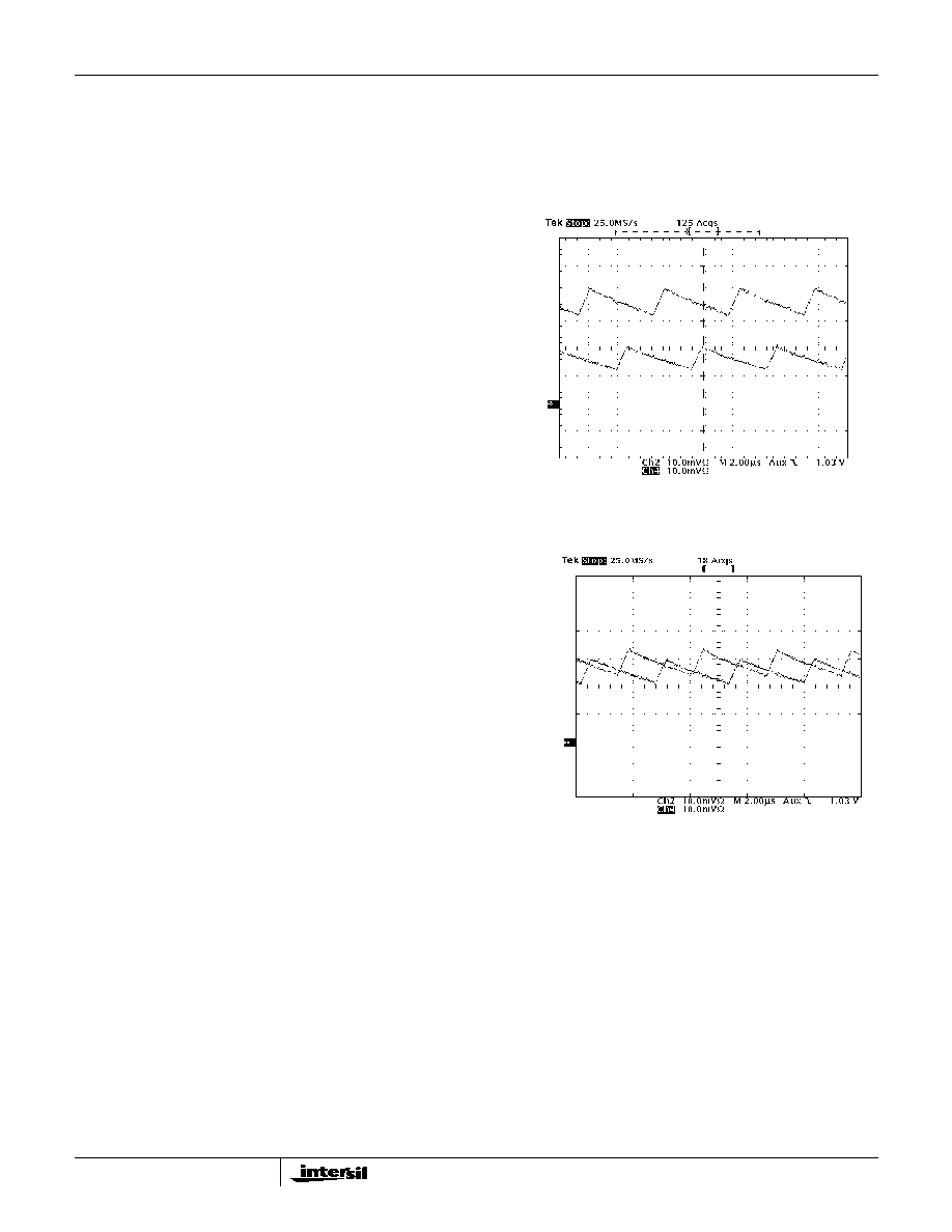
Figures 8 and 9 show the inductor current of a two phase
system without and with current balancing.
Inductor Current
The inductor current in each phase of a multi-phase Buck
converter has two components. There is a current equal to
the load current divided by the number of phases (I
LT
/ n),
and a sawtooth current, (i
PK-PK
) resulting from switching.
The sawtooth component is dependent on the size of the
inductors, the switching frequency of each phase, and the
values of the input and output voltage. Ignoring secondary
effects, such as series resistance, the peak to peak value of
the sawtooth current can be described by:
i
PK-PK
= (V
IN
x V
CORE
- V
CORE
2
) / (L x F
SW
x V
IN
)
Where: V
CORE
= DC value of the output or V
ID
voltage
V
IN
= DC value of the input or supply voltage
L = value of the inductor
F
SW
= switching frequency
Example: For V
CORE
= 1.6V,
V
IN
= 12V,
L = 1.3
µ
H,
F
SW
= 250kHz,
Then i
PK-PK
= 4.3A
The inductor, or load current, flows alternately from V
IN
through Q1 and from ground through Q2. The HIP6301
samples the on-state voltage drop across each Q2 transistor
to indicate the inductor current in that phase. The voltage
drop is sampled 1/3 of a switching period, i/F
SW
, after Q1 is
turned OFF and Q2 is turned on. Because of the sawtooth
current component, the sampled current is different from the
average current per phase. Neglecting secondary effects,
the sampled current (I
SAMPLE
) can be related to the load
current (I
LT
) by:
I
SAMPLE
= I
LT
/ n + (V
IN
V
CORE
-3V
CORE
2
) / (6L x F
SW
x
V
IN
)
0
5
10
15
20
25
AMPERES
FIGURE 8. TWO CHANNEL MULTIPHASE SYSTEM WITH
CURRENT BALANCING DISABLED
0
5
10
15
20
25
AMPERES
FIGURE 9. TWO CHANNEL MULTIPHASE SYSTEM WITH
CURRENT BALANCING ENABLED
HIP6301
HIP6301

13
Where: I
LT
= total load current
n = the number of channels
Example: Using the previously given conditions, and
For I
LT
= 100A,
n = 4
Then I
SAMPLE
= 25.49A
As discussed previously, the voltage drop across each Q2
transistor at the point in time when current is sampled is
r
DSON
(Q2) x I
SAMPLE
. The voltage at Q2's drain, the
PHASE node, is applied through the R
ISEN
resistor to the
HIP6301 ISEN pin. This pin is held at virtual ground, so the
current into ISEN is:
I
SENSE
= I
SAMPLE
x r
DS(ON)
(Q2) / R
ISEN
.
R
Isen
= I
SAMPLE
x r
DS(ON)
(Q2) / 50
µ
A
Example: From the previous conditions,
where I
LT
= 100A,
I
SAMPLE
= 25.49A,
r
DS(ON)
(Q2)
= 4m
Then: R
ISEN
= 2.04K and
I
CURRENT TRIP
= 165%
Short circuit I
LT
= 165A.
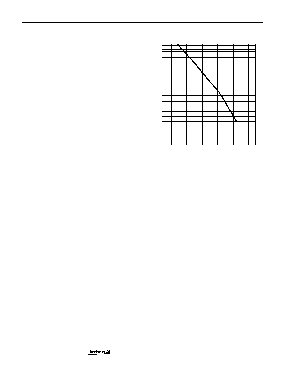
Channel Frequency Oscillator
The channel oscillator frequency is set by placing a resistor,
R
T
, to ground from the FS/DIS pin. Figure 10 is a curve
showing the relationship between frequency, F
SW,
and
resistor R
T
. To avoid pickup by the FS/DIS pin, it is important
to place this resistor next to the pin.
Layout Considerations
MOSFETs switch very fast and efficiently. The speed with
which the current transitions from one device to another
causes voltage spikes across the interconnecting
impedances and parasitic circuit elements. These voltage
spikes can degrade efficiency, radiate noise into the circuit
and lead to device over-voltage stress. Careful component
layout and printed circuit design minimizes the voltage
spikes in the converter. Consider, as an example, the turnoff
transition of the upper PWM MOSFET. Prior to turnoff, the
upper MOSFET was carrying channel current. During the
turnoff, current stops flowing in the upper MOSFET and is
picked up by the lower MOSFET. Any inductance in the
switched current path generates a large voltage spike during
the switching interval. Careful component selection, tight
layout of the critical components, and short, wide circuit
traces minimize the magnitude of voltage spikes. Contact
Intersil for evaluation board drawings of the component
placement and printed circuit board.
There are two sets of critical components in a DC-DC
converter using a HIP6301 controller and a HIP6601 gate
driver. The power components are the most critical because
they switch large amounts of energy. Next are small signal
components that connect to sensitive nodes or supply
critical bypassing current and signal coupling.
The power components should be placed first. Locate the
input capacitors close to the power switches. Minimize the
length of the connections between the input capacitors, C
IN
,
and the power switches. Locate the output inductors and
output capacitors between the MOSFETs and the load.
Locate the gate driver close to the MOSFETs.
The critical small components include the bypass capacitors
for VCC and PVCC on the gate driver ICs. Locate the
bypass capacitor, C
BP
, for the HIP6301 controller close to
the device. It is especially important to locate the resistors
associated with the input to the amplifiers close to their
respective pins, since they represent the input to feedback
amplifiers. Resistor R
T
, that sets the oscillator frequency
should also be located next to the associated pin. It is
especially important to place the R
SEN
resistor(s) at the
respective terminals of the HIP6301.
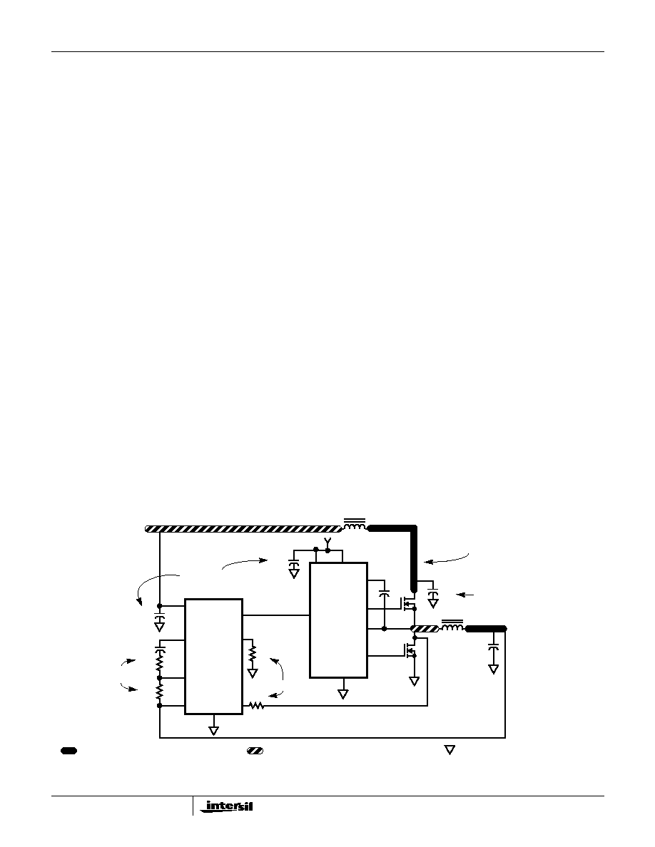
A multi-layer printed circuit board is recommended. Figure 11
shows the connections of the critical components for one output
channel of the converter. Note that capacitors C
IN
and C
OUT
could each represent numerous physical capacitors. Dedicate
one solid layer, usually the middle layer of the PC board, for a
ground plane and make all critical component ground
connections with vias to this layer. Dedicate another solid layer as
a power plane and break this plane into smaller islands of
common voltage levels. Keep the metal runs from the PHASE
terminal to inductor L
O1
short. The power plane should support
the input power and output power nodes. Use copper filled
polygons on the top and bottom circuit layers for the phase nodes.
Use the remaining printed circuit layers for small signal wiring.
50
100
10
20
200
500 1,000
5,000 10,000
2,000
1
2
5
10
20
50
100
200
500
1,000
R
T
(k
)
CHANNEL OSCILLATOR FREQUENCY, F
SW
(kHz)
FIGURE 10. RESISTANCE R
T
vs FREQUENCY
HIP6301

14
The wiring traces from the driver IC to the MOSFET gate and
source should be sized to carry at least one ampere of current.
Component Selection Guidelines
Output Capacitor Selection
The output capacitor is selected to meet both the dynamic
load requirements and the voltage ripple requirements. The
load transient for the microprocessor CORE is characterized
by high slew rate (di/dt) current demands. In general,
multiple high quality capacitors of different size and dielectric
are paralleled to meet the design constraints.
Modern microprocessors produce severe transient load rates.
High frequency capacitors supply the initially transient current
and slow the load rate-of-change seen by the bulk capacitors.
The bulk filter capacitor values are generally determined by
the ESR (effective series resistance) and voltage rating
requirements rather than actual capacitance requirements.
High frequency decoupling capacitors should be placed as
close to the power pins of the load as physically possible. Be
careful not to add inductance in the circuit board wiring that
could cancel the usefulness of these low inductance
components. Consult with the manufacturer of the load on
specific decoupling requirements.
Use only specialized low-ESR capacitors intended for
switching-regulator applications for the bulk capacitors. The
bulk capacitor's ESR determines the output ripple voltage
and the initial voltage drop following a high slew-rate
transient's edge. In most cases, multiple capacitors of small
case size perform better than a single large case capacitor.
Bulk capacitor choices include aluminum electrolytic, OS-
Con, Tantalum and even ceramic dielectrics. An aluminum
electrolytic capacitor's ESR value is related to the case size
with lower ESR available in larger case sizes. However, the
equivalent series inductance (ESL) of these capacitors
increases with case size and can reduce the usefulness of
the capacitor to high slew-rate transient loading.
Unfortunately, ESL is not a specified parameter. Consult the
capacitor manufacturer and measure the capacitor's
impedance with frequency to select a suitable component.
Output Inductor Selection
One of the parameters limiting the converter's response to a
load transient is the time required to change the inductor
current. Small inductors in a multi-phase converter reduces
the response time without significant increases in total ripple
current.
The output inductor of each power channel controls the
ripple current. The control IC is stable for channel ripple
current (peak-to-peak) up to twice the average current. A
single channel's ripple current is approximately:
The current from multiple channels tend to cancel each other
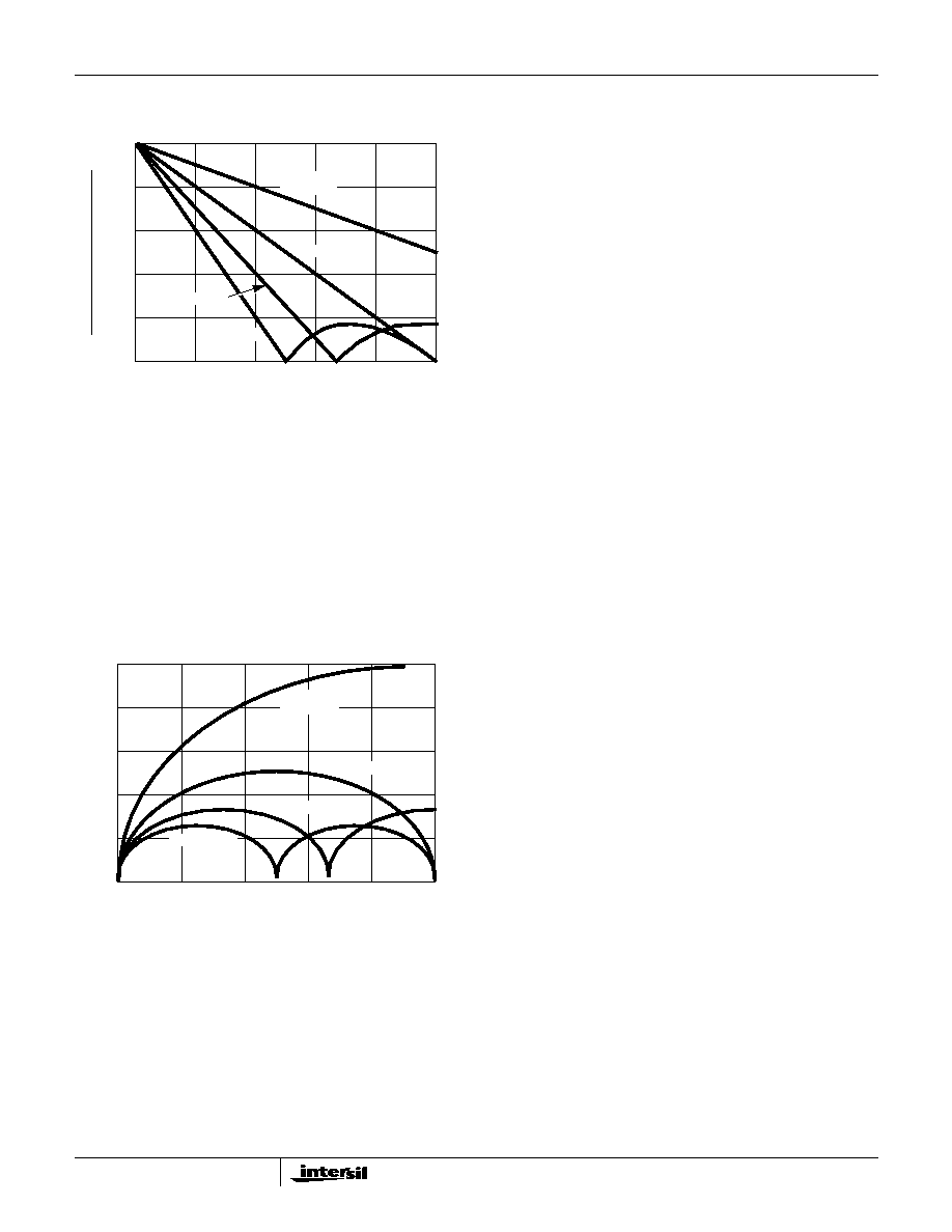
and reduce the total ripple current. Figure 12 gives the total
ripple current as a function of duty cycle, normalized to the
parameter
at zero duty cycle. To determine
the total ripple current from the number of channels and the
duty cycle, multiply the y-axis value by
.
Small values of output inductance can cause excessive
power dissipation. The HIP6303 is designed for stable
operation for ripple currents up to twice the load current.
However, for this condition, the RMS current is 115% above
the value shown in the following MOSFET Selection and
Considerations section. With all else fixed, decreasing the
I
V
IN
V
OUT
≠
F
SW
L
◊
--------------------------------
V
OUT
V
IN
----------------
◊
=
V
CORE
+12V
VIA CONNECTION TO GROUND PLANE
ISLAND ON POWER PLANE LAYER
ISLAND ON CIRCUIT PLANE LAYER
L
O1
C
OUT
C
IN
+5V
IN
KEY
PHASE
VCC
USE INDIVIDUAL METAL RUNS
COMP
HIP6301
PWM
R
T
R
IN
R
FB
C
BP
FB
VSEN
ISEN
R
SEN
HIP6601
C
BOOT
C
BP
C
T
V
CC
FS/DIS
PVCC
LOCATE NEXT TO IC PIN
LOCATE NEXT
TO FB PIN
LOCATE NEXT TO IC PIN(S)
ISOLATE OUTPUT STAGES
FOR EACH CHANNEL TO HELP
LOCATE NEAR TRANSISTOR
FIGURE 11. PRINTED CIRCUIT BOARD POWER PLANES AND ISLANDS
Vo
(
)
LxF
SW
(
)
/
Vo
(
)
LxF
SW
(
)
/
HIP6301
HIP6301

15
inductance could increase the power dissipated in the
MOSFETs by 30%.
Input Capacitor Selection
The important parameters for the bulk input capacitors are
the voltage rating and the RMS current rating. For reliable
operation, select bulk input capacitors with voltage and
current ratings above the maximum input voltage and largest
RMS current required by the circuit. The capacitor voltage
rating should be at least 1.25 times greater than the
maximum input voltage and a voltage rating of 1.5 times is a
conservative guideline. The RMS current required for a
multi-phase converter can be approximated with the aid of
Figure 13.
First determine the operating duty ratio as the ratio of the
output voltage divided by the input voltage. Find the Current
Multiplier from the curve with the appropriate power
channels. Multiply the current multiplier by the full load
output current. The resulting value is the RMS current rating
required by the input capacitor.
Use a mix of input bypass capacitors to control the voltage
overshoot across the MOSFETs. Use ceramic capacitance for
the high frequency decoupling and bulk capacitors to supply
the RMS current. Small ceramic capacitors should be placed
very close to the drain of the upper MOSFET to suppress the
voltage induced in the parasitic circuit impedances.
For bulk capacitance, several electrolytic capacitors
(Panasonic HFQ series or Nichicon PL series or Sanyo
MV-GX or equivalent) may be needed. For surface mount
designs, solid tantalum capacitors can be used, but caution
must be exercised with regard to the capacitor surge current
rating. These capacitors must be capable of handling the
surge-current at power-up. The TPS series available from
AVX, and the 593D series from Sprague are both surge
current tested.
MOSFET Selection and Considerations
In high-current PWM applications, the MOSFET power
dissipation, package selection and heatsink are the
dominant design factors. The power dissipation includes two
loss components; conduction loss and switching loss. These
losses are distributed between the upper and lower
MOSFETs according to duty factor (see the following
equations). The conduction losses are the main component
of power dissipation for the lower MOSFETs, Q2 and Q4 of
Figure 1. Only the upper MOSFETs, Q1 and Q3 have
significant switching losses, since the lower device turns on
and off into near zero voltage.
The equations assume linear voltage-current transitions and
do not model power loss due to the reverse-recovery of the
lower MOSFETs body diode. The gate-charge losses are
dissipated by the Driver IC and don't heat the MOSFETs.
However, large gate-charge increases the switching time,
t
SW
which increases the upper MOSFET switching losses.
Ensure that both MOSFETs are within their maximum
junction temperature at high ambient temperature by
calculating the temperature rise according to package
thermal-resistance specifications. A separate heatsink may
be necessary depending upon MOSFET power, package
type, ambient temperature and air flow.
A diode, anode to ground, may be placed across Q2 and Q4
of Figure 1. These diodes function as a clamp that catches
the negative inductor swing during the dead time between
the turn off of the lower MOSFETs and the turn on of the
upper MOSFETs. The diodes must be a Schottky type to
prevent the lossy parasitic MOSFET body diode from
conducting. It is usually acceptable to omit the diodes and let
the body diodes of the lower MOSFETs clamp the negative
inductor swing, but efficiency could drop one or two percent
as a result. The diode's rated reverse breakdown voltage
must be greater than the maximum input voltage.
1.0
0.8
0.6
0.4
0.2
0
0
0.1
0.2
0.3
0.4
0.5
DUTY CYCLE (V
O
/V
IN
)
RIPPLE CURRENT (A
PEAK-PEAK
)
V
O
/ (L
X
F
SW
)
SINGLE
CHANNEL
2 CHANNEL
3 CHANNEL
4 CHANNEL
FIGURE 12. RIPPLE CURRENT vs DUTY CYCLE
0.5
0.4
0.3
0.2
0.1
0
0
0.1
0.2
0.3
0.4
0.5
DUTY CYCLE (V
O
/V
IN
)
CURRENT MUL
TIPLIER
SINGLE
CHANNEL
3 CHANNEL
4 CHANNEL
2 CHANNEL
FIGURE 13. CURRENT MULTIPLIER vs DUTY CYCLE
P
UPPER
I
O
2
r
DS ON
(
)
◊
V
OUT
◊
V
IN
------------------------------------------------------------
I
O
V
IN
◊
t
SW
◊
F
SW
◊
2
----------------------------------------------------------
+
=
P
LOWER
I
O
2
r
DS ON
(
)
◊
V
IN
V
OUT
≠
(
)
◊
V
IN
---------------------------------------------------------------------------------
=
HIP6301
HIP6301

16
All Intersil semiconductor products are manufactured, assembled and tested under ISO9000 quality systems certification.
Intersil semiconductor products are sold by description only. Intersil Corporation reserves the right to make changes in circuit design and/or specifications at any time with-
out notice. Accordingly, the reader is cautioned to verify that data sheets are current before placing orders. Information furnished by Intersil is believed to be accurate and
reliable. However, no responsibility is assumed by Intersil or its subsidiaries for its use; nor for any infringements of patents or other rights of third parties which may result
from its use. No license is granted by implication or otherwise under any patent or patent rights of Intersil or its subsidiaries.
For information regarding Intersil Corporation and its products, see web site www.intersil.com
Sales Office Headquarters
NORTH AMERICA
Intersil Corporation
P. O. Box 883, Mail Stop 53-204
Melbourne, FL 32902
TEL: (321) 724-7000
FAX: (321) 724-7240
EUROPE
Intersil SA
Mercure Center
100, Rue de la Fusee
1130 Brussels, Belgium
TEL: (32) 2.724.2111
FAX: (32) 2.724.22.05
ASIA
Intersil (Taiwan) Ltd.
7F-6, No. 101 Fu Hsing North Road
Taipei, Taiwan
Republic of China
TEL: (886) 2 2716 9310
FAX: (886) 2 2715 3029
HIP6301
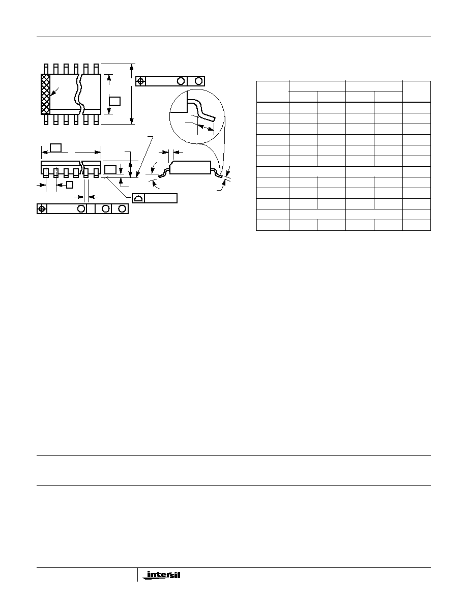
Small Outline Plastic Packages (SOIC)
NOTES:
1. Symbols are defined in the "MO Series Symbol List" in Section 2.2 of
Publication Number 95.
2. Dimensioning and tolerancing per ANSI Y14.5M-1982.
3. Dimension "D" does not include mold flash, protrusions or gate burrs.
Mold flash, protrusion and gate burrs shall not exceed 0.15mm (0.006
inch) per side.
4. Dimension "E" does not include interlead flash or protrusions. Interlead
flash and protrusions shall not exceed 0.25mm (0.010 inch) per side.
5. The chamfer on the body is optional. If it is not present, a visual index
feature must be located within the crosshatched area.
6. "L" is the length of terminal for soldering to a substrate.
7. "N" is the number of terminal positions.
8. Terminal numbers are shown for reference only.
9. The lead width "B", as measured 0.36mm (0.014 inch) or greater
above the seating plane, shall not exceed a maximum value of
0.61mm (0.024 inch)
10. Controlling dimension: MILLIMETER. Converted inch dimensions
are not necessarily exact.
INDEX
AREA
E
D
N
1
2
3
-B-
0.25(0.010)
C A
M
B S
e
-A-
L
B
M
-C-
A1
A
SEATING PLANE
0.10(0.004)
h x 45
o
C
H
0.25(0.010)
B
M
M
M20.3
(JEDEC MS-013-AC ISSUE C)
20 LEAD WIDE BODY SMALL OUTLINE PLASTIC PACKAGE
SYMBOL
INCHES
MILLIMETERS
NOTES
MIN
MAX
MIN
MAX
A
0.0926
0.1043
2.35
2.65
-
A1
0.0040
0.0118
0.10
0.30
-
B
0.013
0.0200
0.33
0.51
9
C
0.0091
0.0125
0.23
0.32
-
D
0.4961
0.5118
12.60
13.00
3
E
0.2914
0.2992
7.40
7.60
4
e
0.050 BSC
1.27 BSC
-
H
0.394
0.419
10.00
10.65
-
h
0.010
0.029
0.25
0.75
5
L
0.016
0.050
0.40
1.27
6
N
20
20
7
0
o
8
o
0
o
8
o
-
Rev. 0 12/93


