1
Æ
FN4902.2
HIP6602A
Dual Channel Synchronous Rectified
Buck MOSFET Driver
The HIP6602A is a high frequency, two power channel
MOSFET driver specifically designed to drive four power
N-Channel MOSFETs in a synchronous rectified buck
converter topology. This device is available in either a 14
lead SOIC or a 16 lead QFN package with a PAD to
thermally enhance the package. These drivers combined
with a HIP63xx or ISL65xx series of Multi-Phase Buck PWM
controllers and MOSFETs form a complete core voltage
regulator solution for advanced microprocessors.
The HIP6602A drives both upper and lower gates over a
range of 5V to 12V. This drive-voltage flexibility provides the
advantage of optimizing applications involving trade-offs
between switching losses and conduction losses.
The output drivers in the HIP6602A have the capacity to
efficiently switch power MOSFETs at high frequencies. Each
driver is capable of driving a 3000pF load with a 30ns
propagation delay and 50ns transition time. This device
implements bootstrapping on the upper gates with only a
single external capacitor required for each power channel.
This reduces implementation complexity and allows the use
of higher performance, cost effective, N-Channel MOSFETs.
Adaptive shoot-through protection is integrated to prevent
both MOSFETs from conducting simultaneously.
Features
∑ Drives Four N-channel MOSFETs
∑ Adaptive Shoot-Through Protection
∑ Internal Bootstrap Devices
∑ Supports High Switching Frequency
- Fast Output Rise Time
- Propagation Delay 30ns
∑ Small 14-Lead SOIC Package
∑ Smaller 16-Lead QFN Thermally Enhanced Package
∑ 5V to 12V Gate-Drive Voltages for Optimal Efficiency
∑ Three-State Input for Bridge Shutdown
∑ Supply Under-Voltage Protection
Applications
∑ Core Voltage Supplies for Intel PentiumÆ III
and AMDÆ
Athlon
TM
Microprocessors.
∑ High Frequency Low Profile DC/DC Converters
∑ High Current Low Voltage DC/DC Converters
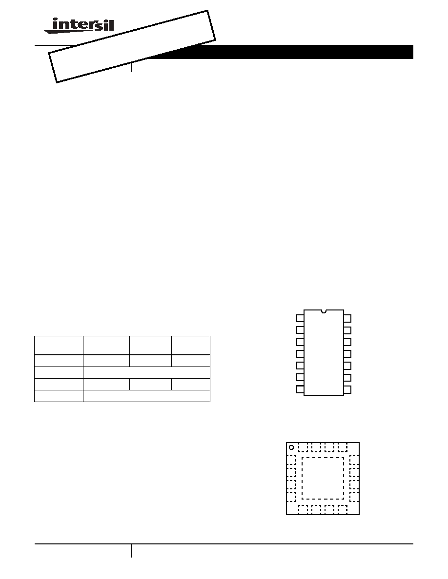
Pinout
HIP6602ACB (SOIC)
TOP VIEW
Ordering Information
PART NUMBER
TEMP. RANGE
(∞C)
PACKAGE
PKG. DWG #
HIP6602ACB
0 to 85
14 Ld SOIC
M14.15
HIP6602ACB-T
14 Ld SOIC Tape and Reel
HIP6602ACR
0 to 85
16 Ld 5x5 QFN L16.5x5
HIP6602ACR-T
16 Ld 5x5 QFN Tape and Reel
PWM1
PWM2
GND
LGATE1
1
2
3
4
14
13
12
PHASE1
UGATE1
BOOT1
PVCC
1
2
10
9
8
7
6
5
BOOT2
UGATE2
PHASE2
VCC
PGND
LGATE2
11
GND
LG1
PVCC
PGND
PWM2
PWM1
VCC
PHAS
E1
UG1
BOOT1
BOOT2
UG2
NC
LG
2
PHASE2
NC
HIP6602ACR (16 LEAD QFN)
TOP VIEW
1
3
4
15
16
14
13
2
12
10
9
11
6
5
7
8
Data Sheet
July 2003
CCAUTION: These devices are sensitive to electrostatic discharge; follow proper IC Handling Procedures.
1-888-INTERSIL or 1-888-468-3774
|
Intersil (and design) is a registered trademark of Intersil Americas Inc.
Copyright © Intersil Americas Inc. 2003. All Rights Reserved. All other trademarks mentioned are the property of their respective owners.
AMDÆ is a registered trademark of Advanced Micro Devices, Inc. AthlonTM is a trademark of Advanced Micro Devices, Inc.PentiumÆ is a registered trademark of Intel Corporation.
NOT
RECO
MME
NDED
FOR
NEW
DES
IGNS
POSS
IBLE
SUB
STITU
TE P
ROD
UCTS
(ISL6
614,
ISL66
14A,
and I
SL66
14B)
2
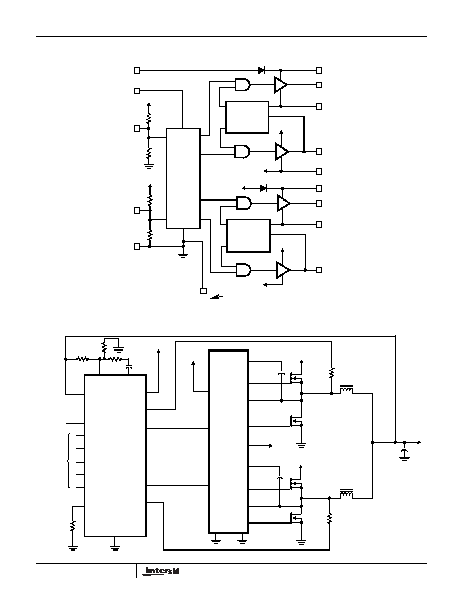
Block Diagram
Typical Application - 2 Channel Converter Using a HIP6302 and a HIP6602A Gate Driver
VCC
PWM1
+5V
10K
10K
CONTROL
LOGIC
SHOOT-
THROUGH
PROTECTION
BOOT1
UGATE1
PHASE1
LGATE1
PGND
PWM2
10K
10K
SHOOT-
THROUGH
PROTECTION
BOOT2
UGATE2
PHASE2
LGATE2
+5V
GND
PVCC
PVCC
PVCC
PVCC
PGND
PGND
HIP6602A
PAD
package MUST be soldered to the PC board
For HIP6602ACR, the PAD on the bottom side of the
MAIN
CONTROL
HIP6302
FB
+5V
COMP
PWM1
PWM2
ISEN2
VSEN
FS/DIS
ISEN1
GND
BOOT2
UGATE2
PHASE2
LGATE2
BOOT1
UGATE1
LGATE1
PWM1
PVCC
+5V/12V
VCC
+12V
DUAL
DRIVER
HIP6602A
PGND
V
CC
+V
CORE
PWM2
PGOOD
VID
+12V
+12V
GND
PHASE1
HIP6602A
3
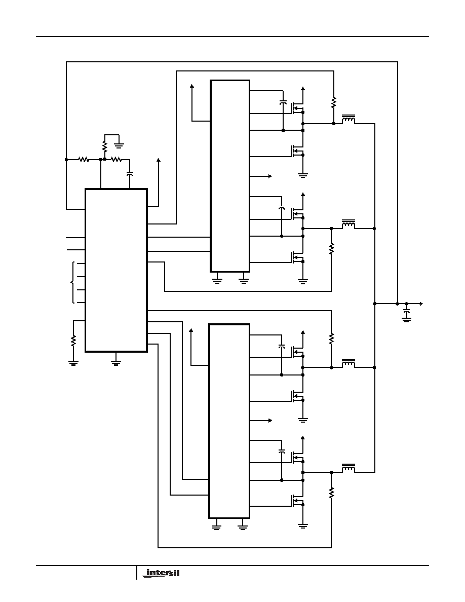
Typical Application - 4 Channel Converter Using a HIP6303 and HIP6602A Gate Driver
MAIN
CONTROL
HIP6303
FB
+5V
COMP
PWM1
PWM2
ISEN2
PWM3
PWM4
ISEN4
VSEN
FS/DIS
ISEN1
ISEN3
GND
BOOT2
UGATE2
PHASE2
LGATE2
BOOT1
UGATE1
PHASE1
LGATE1
PWM1
PVCC
+5V/12V
VCC
DUAL
DRIVER
HIP6602A
BOOT4
UGATE4
PHASE4
LGATE4
BOOT3
UGATE3
PHASE3
LGATE3
PWM3
PVCC
VCC
DUAL
DRIVER
HIP6602A
V
CC
+V
CORE
PWM2
PWM4
EN
VID
PGOOD
+12V
+12V
+12V
+12V
+12V
+5V/12V
+12V
PGND
GND
PGND
GND
HIP6602A
4
Absolute Maximum Ratings
Thermal Information
Supply Voltage (VCC) . . . . . . . . . . . . . . . . . . . . . . . . . . . . . . . . .15V
Supply Voltage (PVCC) . . . . . . . . . . . . . . . . . . . . . . . . . VCC + 0.3V
BOOT Voltage (V
BOOT
- V
PHASE
) . . . . . . . . . . . . . . . . . . . . . . .15V
Input Voltage (VPWM) . . . . . . . . . . . . . . . . . . . . . . GND - 0.3V to 7V
UGATE. . . . . . . . . . . . . . . . . . . . . . V
PHASE
- 0.3V to V
BOOT
+ 0.3V
LGATE . . . . . . . . . . . . . . . . . . . . . . . . .GND - 0.3V to V
PVCC
+ 0.3V
ESD Rating
Human Body Model (Per MIL-STD-883 Method 3015.7) . . . . .3kV
Machine Model (Per EIAJ ED-4701 Method C-111) . . . . . . .200V
Operating Conditions
Ambient Temperature Range. . . . . . . . . . . . . . . . . . . . . 0∞C to 85∞C
Maximum Operating Junction Temperature. . . . . . . . . . . . . . . 125∞C
Supply Voltage, VCC . . . . . . . . . . . . . . . . . . . . . . . . . . . . 12V
±
10%
Supply Voltage Range PVCC . . . . . . . . . . . . . . . . . . . . . 5V to 12V
Thermal Resistance
JA
(∞C/W)
JC
(∞C/W)
SOIC Package (Note 1) . . . . . . . . . . . .
68
NA
QFN Package (Note 2). . . . . . . . . . . . .
36
6
Maximum Junction Temperature (Plastic Package) . . . . . . . . 150∞C
Maximum Storage Temperature Range . . . . . . . . . . -65∞C to 150∞C
Maximum Lead Temperature (Soldering 10s) . . . . . . . . . . . . . 300∞C
(SOIC - Lead Tips Only)
For Recommended soldering conditions see Tech Brief TB389.
CAUTION: Stresses above those listed in "Absolute Maximum Ratings" may cause permanent damage to the device. This is a stress only rating and operation of the
device at these or any other conditions above those indicated in the operational sections of this specification is not implied.
NOTE:
1.
JA
is measured with the component mounted on a high effective thermal conductivity test board in free air. See Tech Brief TB379 for details.
2.
JA
is measured in free air with the component mounted on a high effective thermal conductivity test board with "direct attach" features.
JC,
the
"case temp" is measured at the center of the exposed metal pad on the package underside. See Tech Brief TB379.
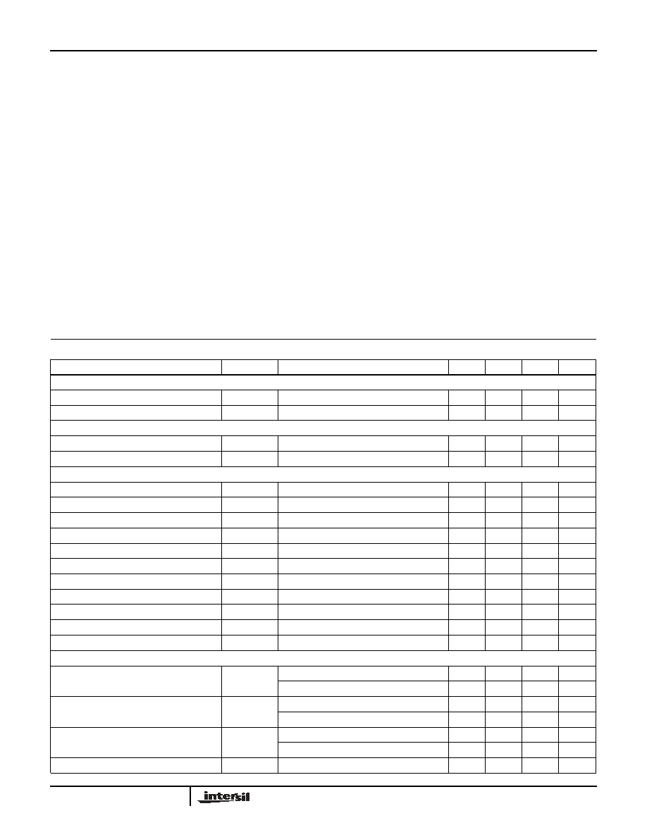
Electrical Specifications
Recommended Operating Conditions, Unless Otherwise Noted
PARAMETER
SYMBOL
TEST CONDITIONS
MIN
TYP
MAX
UNITS
VCC SUPPLY CURRENT
Bias Supply Current
I
VCC
f
PWM
= 500kHz, V
PVCC
= 12V
-
3.7
5.0
mA
Power Supply Current
I
PVCC
f
PWM
= 500kHz, V
PVCC
= 12V
-
2.0
4.0
mA
POWER-ON RESET
VCC Rising Threshold
9.7
9.95
10.4
V
VCC Falling Threshold
9.0
9.2
9.5
V
PWM INPUT
Input Current
I
PWM
V
PWM
= 0 or 5V (See Block Diagram)
-
500
-
µ
A
PWM Rising Threshold
V
PVCC
= 12V
3.45
3.6
-
V
PWM Falling Threshold
V
PVCC
= 12V
-
1.45
1.55
V
UGATE Rise Time
TR
UGATE
V
PVCC
= V
VCC
= 12V, 3nF Load
-
20
-
ns
LGATE Rise Time
TR
LGATE
V
PVCC
= V
VCC
= 12V, 3nF Load
-
50
-
ns
UGATE Fall Time
TF
UGATE
V
PVCC
= V
VCC
= 12V, 3nF Load
-
20
-
ns
LGATE Fall Time
TF
LGATE
V
PVCC
= V
VCC
= 12V, 3nF Load
-
20
-
ns
UGATE Turn-Off Propagation Delay
TPDL
UGATE
V
PVCC
= V
VCC
= 12V, 3nF Load
-
30
-
ns
LGATE Turn-Off Propagation Delay
TPDL
LGATE
V
PVCC
= V
VCC
= 12V, 3nF Load
-
20
-
ns
Shutdown Window
1.4
-
3.6
V
Shutdown Holdoff Time
-
230
-
ns
OUTPUT
Upper Drive Source Impedance
R
UGATE
V
VCC
= 12V, V
PVCC
= 5V
-
1.7
3.0
V
VCC
= V
PVCC
= 12V
-
3.0
5.0
Upper Drive Sink Impedance
R
UGATE
V
VCC
= 12V, V
PVCC
= 5V
-
2.3
4.0
V
VCC
= V
PVCC
= 12V
-
1.1
2.0
Lower Drive Source Current
I
LGATE
V
VCC
= 12V, V
PVCC
= 5V
400
580
-
mA
V
VCC
= V
PVCC
= 12V
500
730
-
mA
Lower Drive Sink Impedance
R
LGATE
V
VCC
= 12V, V
PVCC
= 5V or 12V
-
1.6
4.0
HIP6602A
5
Functional Pin Descriptions
PWM1 (Pin 1) and PWM2 (Pin 2)
The PWM signal is the control input for the driver. The PWM
signal can enter three distinct states during operation, see the
three-state PWM Input section under DESCRIPTION for further
details. Connect this pin to the PWM output of the controller.
GND (Pin 3)
Bias and reference ground. All signals are referenced to this
node.
LGATE1 (Pin 4) and LGATE2 (Pin 7)
Lower gate drive outputs. Connect to gates of the low-side
power N-Channel MOSFETs.
PVCC (Pin 5)
This pin supplies the upper and lower gate drivers bias.
Connect this pin from +12V down to +5V.
PGND (Pin 6)
This pin is the power ground return for the lower gate
drivers.
PHASE2 (Pin 8) and PHASE1 (Pin 13)
Connect these pins to the source of the upper MOSFETs
and the drain of the lower MOSFETs. The PHASE voltage is
monitored for adaptive shoot-through protection. These pins
also provide a return path for the upper gate drive.
UGATE2 (Pin 9) and UGATE1 (Pin 12)
Upper gate drive outputs. Connect to gate of high-side
power N-Channel MOSFETs.
BOOT 2 (Pin 10) and BOOT 1 (Pin 11)
Floating bootstrap supply pins for the upper gate drivers.
Connect the bootstrap capacitor between these pins and the
PHASE pin. The bootstrap capacitor provides the charge to
turn on the upper MOSFETs. See the Internal Bootstrap
Device section under DESCRIPTION for guidance in
choosing the appropriate capacitor value.
VCC (Pin 14)
Connect this pin to a +12V bias supply. Place a high quality
bypass capacitor from this pin to GND. To prevent forward
biasing an internal diode, this pin should be more positive
then PVCC during converter start-up.
Description
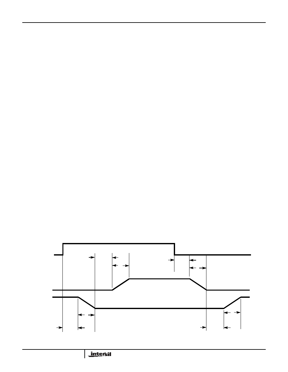
Operation
Designed for versatility and speed, the HIP6602A two channel,
dual MOSFET driver controls both high-side and low-side
N-Channel FETs from two externally provided PWM signals.
The upper and lower gates are held low until the driver is
initialized. Once the VCC voltage surpasses the VCC Rising
Threshold (See Electrical Specifications), the PWM signal
takes control of gate transitions. A rising edge on PWM
initiates the turn-off of the lower MOSFET (see Timing
Diagram). After a short propagation delay [TPDL
LGATE
], the
lower gate begins to fall. Typical fall times [TF
LGATE
] are
provided in the Electrical Specifications section. Adaptive
shoot-through circuitry monitors the LGATE voltage and
determines the upper gate delay time [TPDH
UGATE
] based
on how quickly the LGATE voltage drops below 2.2V. This
prevents both the lower and upper MOSFETs from
conducting simultaneously or shoot-through. Once this delay
period is complete the upper gate drive begins to rise
[TR
UGATE
] and the upper MOSFET turns on.
Timing Diagram
PWM
UGATE
LGATE
TPDL
LGATE
TF
LGATE
TPDH
UGATE
TR
UGATE
TPDL
UGATE
TF
UGATE
TPDH
LGATE
TR
LGATE
HIP6602A