1
TM
HIP9010
Engine Knock Signal Processor
The HIP9010 is used to provide a method of detecting
premature detonation or "Knock" in automotive engines.
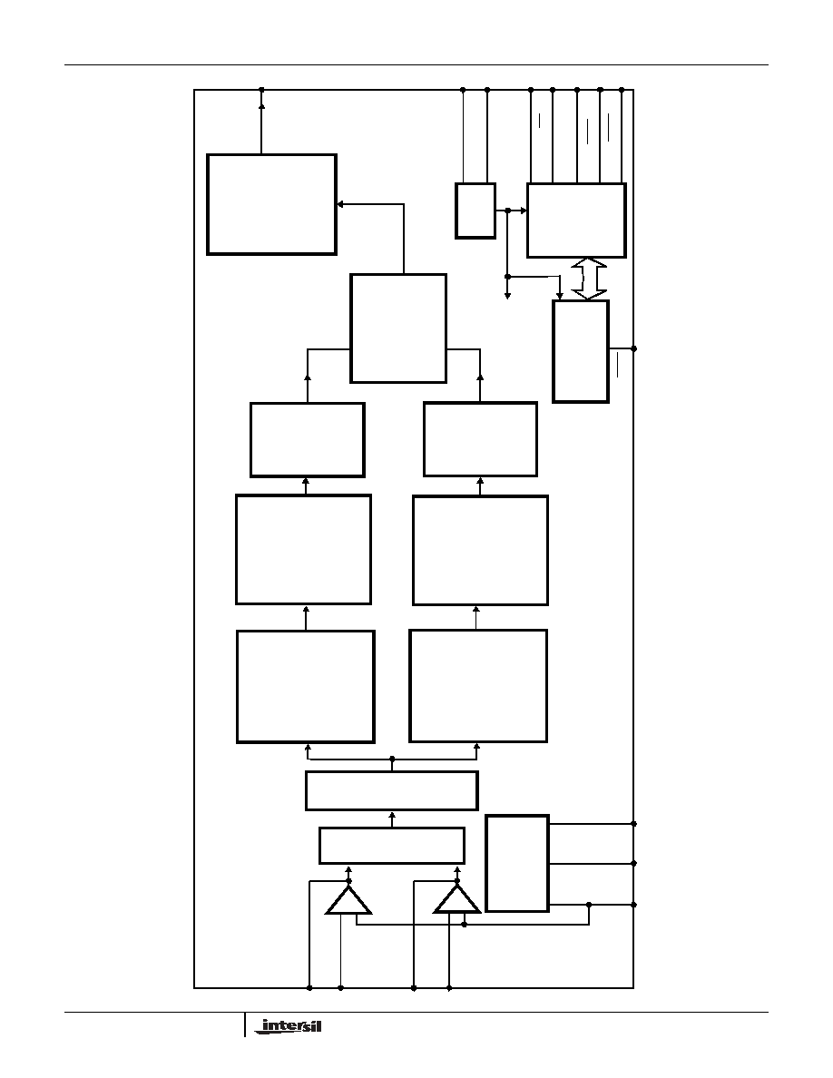
A block diagram of this IC is shown in Figure 1. The chip
alternately selects one of the two sensors mounted on the
engine block. Two programmable bandpass filters process
the signal from both sensors, and divides the signal into two
channels. When the engine is not knocking, programmable
gain adjust stages are set to ensure that both the reference
channel and the knock channel contain similar energies.
This technique ensures that the detection system is
comparatively immune to changes in the engine background
noise level. When the engine is knocking, the energy in the
knock channel increases.
Features
∑ Two Sensor Inputs
∑ Microprocessor Programmable
∑ Accurate and Stable Filter Elements
∑ Digitally Programmable Gain
∑ Digitally Programmable Time Constants
∑ Digitally Programmable Filter Characteristics
∑ On-Chip Clock
∑ Operating Temperature Range -40
o
C to 125
o
C
Applications
∑ Engine Knock Detector Processor
∑ Analog Signal Processing where Controllable Filter
Characteristics are Required
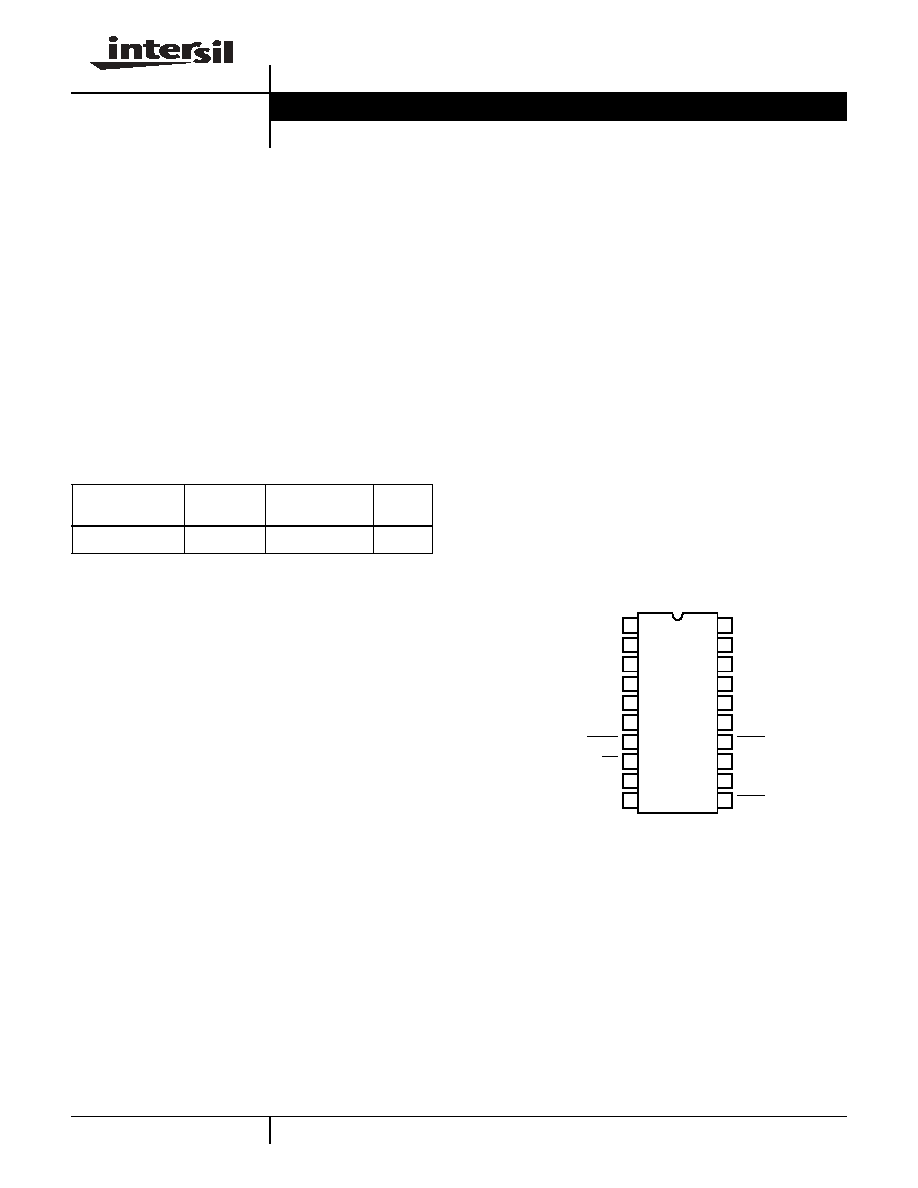
Pinout
HIP9010
(SOIC)
TOP VIEW
Ordering Information
PART NUMBER
TEMP.
RANGE (
o
C)
PACKAGE
PKG.
NO.
HIP9010AB
-40 to 125
20 Ld SOIC (W)
M20.3
11
12
13
14
15
16
17
18
20
19
10
9
8
7
6
5
4
3
2
1
V
DD
GND
V
MID
INOUT
NC
NC
CS
INT/HOLD
OSCIN
OSCOUT
S0IN
S1FB
S1IN
NC
S0FB
NC
TEST
SCK
MOSI
MISO
Data Sheet
November 1998
FN3601.4
CAUTION: These devices are sensitive to electrostatic discharge; follow proper IC Handling Procedures.
1-888-INTERSIL or 321-724-7143
|
Intersil (and design) is a trademark of Intersil Americas Inc.
Copyright © Intersil Americas Inc. 2002. All Rights Reserved
2
H
I
P
901
0
Simplified Block Diagram
ANT
IAL
I
AS
ING
FI
LT
E
R
3
RD O
RDE
R
-
+
-
+
KNOCK FREQUENCY CHANNEL
REFERENCE FREQUENCY CHANNEL
TO SWITCHED
CAPACITOR
NETWORKS
(14) TEST
PROGRAMMABLE
BANDPASS
FILTER
1-20kHz
64 STEPS
PROGRAMMABLE
GAIN
STAGE
1-0.133
64 STEPS
PROGRAMMABLE
BANDPASS
FILTER
1-20kHz
64 STEPS
PROGRAMMABLE
GAIN
STAGE
1-0.133
64 STEPS
ACTIVE
FULL WAVE
RECTIFIER
REGISTERS
AND
STATE MACHINE
SPI
INTERSPACE
POWER SUPPLY
AND
BIAS CIRCUITS
(17) S1IN
(18) S1FB
(20) S0IN
(19) S0FB
(2) GND
OSCIN (9)
OSCOUT (10)
SCK (13)
CS (8)
MOSI (12)
MISO (11)
INT/HOLD (7)
DIFFERENTIAL
TO
SINGLE-ENDED
CONVERTER
AND OUTPUT
DRIVER
PROGRAMMABLE
INTEGRATOR
40-600
µ
s
32 STEPS
ACTIVE
FULL WAVE
RECTIFIER
INOUT (4)
(1) V
DD
(3) V
MID
CLOCK
CHANNE
L
S
E
L
E
CT
S
W
IT
CHE
S
FIGURE 1.
3
Absolute Maximum Ratings
Thermal Information
DC Logic Supply, V
DD
. . . . . . . . . . . . . . . . . . . . . . . . -0.5V to +7.0V
Output Voltage, V
O
. . . . . . . . . . . . . . . . . . . . . . . . . . -0.5V to +7.0V
Input Voltage, V
IN
. . . . . . . . . . . . . . . . . . . . . . . . . . . . . . +7V (Max)
Operating Conditions
Temperature Range. . . . . . . . . . . . . . . . . . . . . . . . . -40
o
C to 125
o
C
Thermal Resistance (Typical, Note 1)
JA
(
o
C/W)
SOIC Package . . . . . . . . . . . . . . . . . . . . . . . . . . . . .
115
Maximum Storage Temperature Range, T
STG
. . . . -65
o
C to 150
o
C
Maximum Junction Temperature . . . . . . . . . . . . . . . . . . . . . . . 150
o
C
Maximum Lead Temperature (Soldering) . . . . . . . . . . . . . . . 300
o
C
At distance 1/16in
±
1/32in (1.59mm
±
0.79mm) from case
for 10s (Max) (SOIC - Lead Tips Only)
CAUTION: Stresses above those listed in "Absolute Maximum Ratings" may cause permanent damage to the device. This is a stress only rating and operation of the
device at these or any other conditions above those indicated in the operational sections of this specification is not implied.
NOTE:
1.
JA
is measured with the component mounted on an evaluation PC board in free air.
Electrical Specifications
V
DD
= 5V,
±
5%, GND = 0V, Clock Frequency 4MHz,
±
0.5%, T
A
= -40
o
C to 125
o
C,
Unless Otherwise Specified
PARAMETER
SYMBOL
TEST CONDITIONS
MIN
TYP
MAX
UNITS
DC ELECTRICAL CHARACTERISTICS
Quiescent Supply Current
I
DD
V
DD
= 5.25V, GND = 0V
3
7.5
12
mA
Midpoint Voltage, Pin 3
V
MID
V
DD
= 5.0V, I
L
= 2mA Source
2.3
2.45
2.55
V
Midpoint Voltage, Pin 3
V
MID
V
DD
= 5.0V, I
L
= 0mA
2.4
2.5
2.6
V
Input Leakage, Pin 14
IL
TEST
Measured at V
DD
= 5.0V
-
-
3
µ
A
Internal Pull-Up Resistance, Pin 14
R
TEST
V
DD
= 5.0V, I Measure = 15
µ
A
30
100
200
K
Leakage of Pins 7, 8, 12 and 13
I
L
Measured at GND and V
DD
= 5V
-
-
±
3
µ
A
Low Input Voltage, Pins 7, 8, 12 and 13
V
IL
-
-
30
% of V
DD
High Input Voltage, Pins 7, 8, 12 and 13
V
IH
70
-
-
% of V
DD
Low Level Output, Pin 11
V
OL
I
SOURCE
= 4mA
0.01
-
0.30
V
Leakage Pin 11
I
L
Measured at GND and V
DD
= 5V
-
-
±
10
µ
A
Low Level Output, Pin 10
V
OL
I
SOURCE
= 500
µ
A, V
DD
= 5V
-
-
1.5
V
High Level Output, Pin 10
V
OH
I
SINK
= -500
µ
A, V
DD
= 5V
4.4
-
-
V
INPUT AMPLIFIERS
S0FB and S1FB High Output Voltage
V
OUT
HI
100
µ
A I
SINK
, V
DD
= 5V
4.7
4.9
-
V
S0FB and S1FB Low Output Voltage
V
OUT
LO
100
µ
A I
SOURCE
, V
DD
= 5V
-
15
200
mV
S0FB and S1FB Closed Loop
A
CL
Input Resistor = 1M
,
Feedback Resistor = 49.9k
-25
-26
-27
dB
S0FB and S1FB Closed Loop
A
CL
Input Resistor = 47.5k
,
Feedback Resistor = 475k
18
20
21
dB
ANTIALIASING FILTER
Response 1kHz to 20kHz,
Referenced to 1kHz
BW
Test Mode, 70mV
RMS
Input to S0FB or
S1FB, Output Pin 4
-
-2
-
dB
Attenuation at 180kHz
Referenced to 1kHz
ATEN
Test Mode, 70mV
RMS
Input to S0FB or
S1FB, Output Pin 4
-10
-15
-
dB
PROGRAMMABLE FILTERS
Peak to Peak Voltage Output
V
OUTP-P
Run Mode
3.5
4.0
-
V
P-P
Filters Q (Note 2)
Q
Run Mode
-
2.5
-
Q
PROGRAMMABLE GAIN AMPLIFIERS
Percent Amplifier Gain Deviation
Per Table 2
%G
Run Mode
-
±
1
-
%
HIP9010
4
INTEGRATOR
Integrator Offset Voltage
INTGV
IO
By Design
-
0.1
-
mV
Integrator Reset Voltage
V
RESET
Pin 4 Voltage at Initiation of
Integration Cycle. V
DD
= 5V
430
500
570
mV
Integrator Droop after 500
µ
s
V
DROOP
Hold Mode, Pin 7 = 0V, V
DD
= 5V,
Pin 4 set to 20% to 80% of V
DD
-
±
±
3
±
±
50
mV
OUTPUT AND SAMPLE AND HOLD
Differential to Single Ended
Converter Offset Voltage
DIFV
IO
By Design
-
0.1
-
mV
Change in Converter Output
DIFOUT
Run Mode, 500
µ
A, Sinking to No Load
-
±
±
1
±
±
3
mV
SYSTEM GAIN DEVIATION
Gain Deviation from "Ideal Equation"
Correlation, Factor - 5.0%
V
OUT
-
V
RESET
Run Mode, maximum signal output
from Input Amplifier <2.25V
P-P
,
Equation Output x 0.95 +
Device
Reset Voltage. For Total V
OUT
4.7V
-8%,
±
±
100mV
Equation
x 0.95
-V
RESET
8%,
±
100mV
V
NOTE:
2. Q = f
O
/BW, Where: f
O
= Center Frequency, BW = 3dB bandwidth.
Ideal Equation
When the two filters are set to the same frequency and the input signal is present for the periods T
IN
, then:
G
R
and G
K
= Programed Gain of Reference and Knock channels.
T
IN
= Time input signal is present In ms.
T
C
= Programmed integrator time constant ms.
N = Number of cycles of input signal.
f
Q
= Frequency of input signal. Assumes both filters are programmed to the same frequency.
V
RESET
= Integrator Reset Voltage.
1.273 = 4/
R
F
= Feedback resistor value.
R
IN
= Signal input resistor value.
For example, assume 300mV
P-P
input with the time constant programmed to 300
µ
s and the Integration time is 1.2ms. The R
F
/R
IN
ratio is one and
the Reference channel is programmed to a Gain of 0.188. The Knock channel is then automatically set to a gain of one. The input signal is contin-
uous for the total integration time, T
IN
.
Electrical Specifications
V
DD
= 5V,
±
5%, GND = 0V, Clock Frequency 4MHz,
±
0.5%, T
A
= -40
o
C to 125
o
C,
Unless Otherwise Specified (Continued)
PARAMETER
SYMBOL
TEST CONDITIONS
MIN
TYP
MAX
UNITS
INTOUT volts
(
)
Input
signal
(V
P P
≠
)
R
F
R
IN
----------
◊
G
K
1.273
N
TC (ms) f
Q
(kHz)
◊
---------------------------------------------------
◊
◊
G
R
1.273
N
TC (ms) f
Q
(kHz)
◊
---------------------------------------------------
◊
◊
≠
V
RESET
+
=
INTOUT volts
(
)
Input
signal
(V
P P
≠
)
R
F
R
IN
----------
◊
1.273
T
IN
TC
---------
G
K
G
R
≠
(
)
◊
V
RESET
+
=
INTOUT volts
(
)
0.3V
(V
P P
≠
)
1.273
1.2ms
0.300ms
-----------------------
1.000 0.188
≠
(
)
◊
◊
◊
V
RESET
1.24V 0.500V
1.74V
=
+
=
+
=
HIP9010
5
+5V
HIP9010
MICROPROCESSOR
SPI BUS
C3, 0.022
µ
F
C2, 3.3nF
C1, 3.3nF
R1
R4
R3
4MHz
A/D
CONVERTER
V
DD
V
MID
GND
S1IN
S1FB
S0IN
S0FB
OSCIN
OSCOUT
INTOUT
MOSI
MISO
SCK
CS
INT/HOLD
TEST
TRANSDUCERS
R2
FIGURE 2. SIMPLIFIED BLOCK DIAGRAM OF THE HIP9010 IN AN AUTOMOTIVE APPLICATION
20pF
20pF
1M
Pin Descriptions
PIN
NUMBER
SYMBOL
DESCRIPTION
1
V
DD
5V power input.
2
GND
This terminal is tied to ground.
3
V
MID
This terminal is tied to the internal mid-supply generator and is brought out for supply bypassing by a 0.022
µ
F
capacitor.
4
INTOUT
Buffered output of the integrator.
5 and 6
NC
These terminals are not internally connected. DO NOT USE.
7
INT/HOLD
Selects whether the chip is in the Integrate Mode (Input High) or in the Hold Mode (Input Low).
8
CS
A low input on this pin enables the chip to communicate over the SPI bus.
9
OSCIN
Input to inverter used for the oscillator circuit. A 4MHz crystal or ceramic resonator is connected between this
pin and pin 10. To bias the inverter, a 1.0M
to 10M
resistor is usually connected between this pin and pin 10.
10
OSCOUT
Output of the inverter used for the oscillator. See pin 9 above.
11
MISO
Output of the chip SPI data bus. It is the inversion of the chip DATAIN line. This is an open drain output. The
output must be disabled by placing the CS High when the chip is not selected.
12
MOSI
Input of the chip SPI data bus. Data length is eight bits.
13
SCK
Input from the SPI clock. Normally high, the data is clocked to the chip internal circuitry on the rising clock edge.
14
TEST
A low on this pin places the chip in the test mode. For normal operation this terminal is tied high or left open.
15 and 16
NC
These terminals are not internally connected. DO NOT USE.
17
S1IN
Inverting input to sensor one amplifier. A resistor is tied from this summing input to the transducer. A second
resistor is tied between this terminal and terminal 18, S1FB to establish the gain of the amplifier.
18
S1FB
Output of the sensor one amplifier. This terminal is used to apply feedback.
19
S0FB
Output of the sensor zero amplifier. This terminal is used to apply feedback.
20
S0IN
Inverting input to sensor zero amplifier. A resistor is tied from this summing input to the transducer. A second
resistor is tied between this terminal and terminal 19, S0FB to establish the gain of the amplifier.
HIP9010
6
Description of the HIP9010 Operation
This IC is designed to be a universal digitally controlled,
analog interface between engine acoustical sensors or
accelerometers and internal combustion engine fuel
management systems. Two wideband input amplifiers are
provided that allow the use of two sensors that may be of the
piezoelectric type that can be mounted in optimum locations
on either in-line or V-type engine configurations.
Output from these amplifiers is directed from a channel
select switch into both digitally controlled filter and amplifier
channels. Both filter bandpass and gain settings are
programmable from a microprocessor. Output from the two
channels is combined in a digitally programmable integrator.
Integrator output is applied to a line driver for further
processing by the engine fuel management system.
Broadband piezoelectric ceramic transducers used for the
engine signal pickup have device capacitances in the order
of 1100pF and output voltages that range from 5mV to
8V
RMS.
During normal engine operation a single input
channel is selected and applied to the filters. One filter
channel processes a signal that is used to establish the
background reference level. The second channel is used to
observe the engine during the time interval that preignition
may be expected. This information is compared with the
"background" signal via the IC's integrator and will tend to
cancel the background noise and accentuate noise due to
engine pre-detonation. Moreover, the bandpass of filter
channels can be optimized to further discriminate between
engine background and combustion noise and
pre-detonation noise.
A basic approach to engine pre-detonation systems is to only
observe engine background during the time interval that noise
is expected and if detected, retard timing. This approach does
not require the sensitivity and selectivity that is needed for a
continuously adjustable solution. Enhanced fuel economy and
performance is obtainable when this IC is coupled with a
microprocessor controlled fuel management system.
Circuit Block Description
Input Amplifiers
Two amplifiers are used to interface to the two engine
sensors. These amplifiers have a typical open loop gain of
100dB, with a typical bandwidth of 2.6MHz. The common
mode input voltage range extends to within 0.5V of either
supply rail. The amplifier output has a similar output range.
Sufficient gain, bandwidth and output swing capability was
provided to ensure that the amplifiers can handle attenuation
gain settings of 20 to 1 or -26dB. This would be needed
when high peak output signals, in the range of 8V
RMS
, are
obtained from the transducer. Gain settings of 10 times can
also be needed when the transducers have output levels of
5mV
RMS
.
In a typical application the input signal frequency may vary
from DC to 20kHz. External capacitors are used to decouple
the IC from the sensor (C1 and C2). A typical value of the
capacitors is 3.3nF. Series input resistors, R1 and R2, are
used to connect the inverting inputs of the amplifiers, (pins
20 and 17). Feedback resistors, R3 and R4, in conjunction
with R1 and R2 are used to set the gain of the amplifiers.
A mid-voltage level is generated by the IC. This level is set to
be half way between V
DD
and ground. Throughout the IC
this level is used as a quiet, DC reference for the circuits
within the IC. This point is brought out for several reasons: it
can be used as a reference voltage, and it must be
bypassed to ensure that it is a quiet reference for the internal
circuitry.
The input amplifiers are designed with power down capability,
which, when activated disables their bias circuit and their
output goes into a three-state condition. This is very important
during the test mode, in which the output terminals of the
amplifiers are driven by the outside world with test signals.
Antialiasing Filter
The IC has a 3rd order Butterworth filter with a -3dB point at
70kHz. Double poly-silicon capacitors and implanted
resistors are used to set poles in the filter. This filter is
required to have no more than 1dB attenuation at 20kHz
(highest frequency off interest) and a minimum attenuation
of 10dB at 180kHz. This filter precedes the switch capacitor
filters which run at 200kHz.
Programmable Band Pass Switched Capacitor Filters
Two identical programmable filters are used to detect the two
frequencies of interest. The Knock Frequency Filter is
programmed to pass the frequency component of the engine
knock. The Reference Frequency Filter is used to detect
background noise at a second programmed frequency. The filter
frequency is established by the characteristics of the particular
engine and transducer. By subtracting the energy component of
these two filters, we can detect if a knock has occurred.
The filters have a nominal differential gain of 4. Their
frequency is set by program words (discussed in the
Communications Protocol section). Center frequencies can
0
SENSOR
C1
R1
R3
PIN 20
V
MID
PIN 3
-
+
PIN 19
1
SENSOR
C2
R2
R4
PIN 17
V
MID
PIN 3
-
+
PIN 18
FIGURE 3. INPUT AMPLIFIER CONNECTIONS
HIP9010

7
be programmed from 1.22kHz to 19.98kHz, in 64 steps. The
filter Qs are typically 2.4.
Balance/Gain Adjust Stage
The gains from the Knock Frequency Filter and the
Reference Frequency Filter can be adjusted with respect to
one another, so that the difference energies in the two bands
can be compensated. This balance is achieved by feeding
one of the filters unattenuated (gain = 1) and attenuating the
other. This can be adjusted with 64 different gain settings,
ranging between 1 and 0.133. The signals can swing
between 20 and 80 percent of V
DD
.
Programming is discussed in the Communications Protocol
section. The test/channel attenuate word is used to
determine which of the two channels is attenuated and
which is set to unity gain.
Active Full Wave Rectifier
The output of the filters are independently full wave rectified
using switch capacitor techniques. Each of two rectifier
circuits provide both negative and positive values for the
knock frequency and reference frequency filter outputs. The
output is able to swing from 20% to 80% of V
DD
. Care was
taken to minimize the RMS variations from input to output of
this section.
Integrator Stage
The signals from the two rectifiers are summed and
integrated together. A differential system is used to reduce
noise. One system integrates the positive energy of the
Knock Frequency Rectifier with respect to the positive
energy of the Reference Frequency Rectifier. The second
system does the integration of the negative energy value of
the two rectifiers. The positive and negative energy signals
are opposite phase signals. Using this technique reduces
system noise.
The integrator time constant is software programmable by
the Integrator Time Constant discussed in the
Communications Protocol section. The time constant can be
programmed from 40
µ
s to 600
µ
s, with a total of 32 steps. If
for example, we program a time constant to 200
µ
s, then with
one volt difference between each channel, the output of the
integrator will change by 1 volt in 200
µ
s.
When integration is enabled by the rising edge of the
INT/HOLD input, the output of the integrator will fall to 0.5V,
within 20
µ
s after the integrate line reaches the integrate
state. The output of the integrator is an analog voltage.
Test Multiplexer
This circuit receives the positive and negative outputs from
the two integrators, together with the outputs from different
parts of the IC. The output is controlled by the fifth
programming word of the communications protocol. This
multiplexes the switch capacitor filter output, the gain control
output and the antialiasing filter output.
Differential to Single-Ended Converter
This signal takes the output of the two integrators (through
the test-multiplexer circuit) and provides a signal that is the
sum of the two signals. This technique is used to improve
the noise immunity of the system.
Output Buffer
This output amplifier is the same amplifier circuits as the
input amplifier used to interface with the sensors. When the
output of the antialiasing filter is tested, this amplifier is in the
power down mode.
Communications Protocol
The multiprocessor talks to the knock sensor via an SPI
bus (MOSI). A chip select pin (CS) is used to enable the
chip, which, in conjunction with the SPI clock (SCK), moves
in the eight bit programming word. Five different
programming words are used to set gains, frequency
response, integrator constants, test mode, channel select
and test mode conditions.
With chip select (CS) going low, on the next rising edge of
the SPI clock (SCK), data is latched into the IC. The data is
shifted with the most significant bit first and least significant
bit last. Each word is divided into two parts: first the address
and then the value. Depending on the function being
controlled, the address is 2 or 3 bits, and the value is either 5
or 6 bits long. During the hold mode of operation, all five
programming words can be entered into the IC, but during
the integrate time any single byte may be entered but will not
be acted upon until the start of the next hold period. The
integration or hold mode of operation is controlled by the
INT/HOLD input signal.
Programming Words
1. Reference Filter Frequency: Defines the center frequency
of the Reference Filter in the system. The first 2 bits are
used for the address and the last 6 bits are used for its
value. 01FFFFFF Example: 01001010 would be the
reference filter (01 for the first two bits) at a center
frequency of 1.78kHz (bit value in Table 2 of 10).
2. Knock Filter Frequency: Defines the center frequency of
the Knock Filter in the system. The first 2 bits are used for
the address and the last 6 bits are used for its value.
00FFFFFF Example: 00100111 would be the knock filter
frequency (00 for the first two bits) at a center frequency
of 6.37kHz (bit value in Table 2 of 39).
3. Balance Control: Defines the ratio of the gain of the knock
band center frequency to that of the reference band
center frequency. This role can be reversed by the value
of C
A
in the fifth programming bit, as explained in 5,
Test/Channel Select/Channel Attenuate Control. The first
2 bits are used for the address and the last 6 bits for its
value. 10GGGGGG Example: 10010100 would be the
balance control (10 for the first two bits) with an
attenuation of 0.514 (bit value in Table 2 of 20.)
Depending on the value of C
A
in the fifth word this would
apply to the reference or the knock gain section.
HIP9010
8
4. Integrator Time Constant: Defines the Integration Time
Constant for the system. The first 3 bits are used for the
address and the last 5 bits for the value. 110TTTTT
Example: 11000011 would be the integrator time
constant (110 on for the first 3 bits) and an integration
constant of 55
µ
s (bit value of 3 in Table 2).
5. Test/Channel Select/Channel Attenuate Control: This word
serves several purposes. By looking at the structure,
111T
A
T
B
T
C
C
S
C
A
, the first 3 bits are used for the address,
and the last 5 bits are used for the value. The options are:
- If CS is "0" channel "0" is selected. If CS is "1" channel "1"
is selected.
- If C
A
is "0" attenuation applies to the knock filter. If C
A
is
"1" attenuation applies to the reference filter.
- During the test mode (TEST input is a low level), if T
A
is "0"
all sections get their input from the output of the
antialiasing filter input. This input can come from either the
output of channel "0" amplifier or channel "1" output
depending upon the state of the C
S
bit. If T
A
is "0" the input
amplifiers are powered down. If T
A
is set to "1" during the
test mode the chip is configured in its normal operating
state, getting inputs to all sections from previous sections.
- Combinations of T
A
, T
B
and T
C
are used to test the
different analog parts of the circuit. Table 1 shows these
combinations. All blocks except for the antialiasing filter
are sampled via the differential to single ended converter
in the test mode.
TABLE 1. SHOWING PROGRAMMING IN THE TEST MODE
TEST
PIN 14
T
A
T
B
T
C
C
HS
ANALOG OUTPUT
FROM:
0
0
0
0
0
Knock Rectifier
0
0
0
0
1
Reference
0
0
0
1
0
Knock Filter
0
0
0
1
1
Reference Filter
0
0
1
0
0
Antialias Filter(1)
0
0
1
0
1
Antialias Filter(1)
0
0
1
1
0
Integrator
0
0
1
1
1
Integrator
0
1
0
0
0
Knock Rectifier
0
1
0
0
1
Reference
0
1
0
1
0
Knock Filter
0
1
0
1
1
Reference Filter
0
1
1
0
0
Antialias Filter(1)
0
1
1
0
1
Antialias Filter(1)
0
1
1
1
0
Integrator
0
1
1
1
1
Integrator
1
x
x
x
x
Integrator
NOTE:
3. All Test function blocks have their outputs buffered by the differential
to single ended converter. Their outputs are available at the
INTOUT pin 4 of the chip. In the case of the antialias filter test
function, the output is taken directly to the INTOUT pin 4 of the chip.
FIGURE 4A. S0IN AND S1IN INPUT CIRCUIT
FIGURE 4B. MISO OUTPUT OF SPI DATA BUS IS AN OPEN
DRAIN TRANSISTOR
FIGURE 4C. TEST PMOS TRANSISTOR HAS EQUIVALENT
CURRENT PULLUP CAPABILITY OF A 50k TO
200k RESISTOR
FIGURE 4D. S0FB, S1FB AND INOUT EQUIVALENT OUTPUT
CIRCUITS
FIGURE 4. INTERFACE CIRCUITS
S0IN
S1IN
TO NEXT STAGE
HALF OF
DIFFERENTIAL
AMPLIFIER
V
DD
MISO
11
V
DD
TEST
14
TO LOGIC
50
µ
A
V
DD
S0FB S1FB
INOUT
HIP9010
9
TABLE 2. FREQUENCY, BALANCE / GAIN AND INTEGRATOR TIME CONSTANT SETTINGS
BIT VALUE PER
FUNCTION
FREQUENCY
kHz
OUTPUT
LEVEL
TIME
CONSTANT
µ
s
BIT VALUE PER
FUNCTION
FREQUENCY
kHz
OUTPUT
LEVEL
0
1.22
1.000
40
32
4.95
0.360
1
1.26
0.960
45
33
5.12
0.346
2
1.31
0.923
50
34
5.29
0.333
3
1.35
0.889
55
35
5.48
0.320
4
1.40
0.857
60
36
5.68
0.309
5
1.45
0.828
65
37
5.90
0.298
6
1.51
0.800
70
38
6.12
0.288
7
1.57
0.774
75
39
6.37
0.279
8
1.63
0.750
80
40
6.64
0.270
9
1.71
0.727
90
41
6.94
0.262
10
1.78
0.706
100
42
7.27
0.254
11
1.87
0.686
110
43
7.63
0.247
12
1.96
0.667
120
44
8.02
0.240
13
2.07
0.649
130
45
8.46
0.234
14
2.18
0.632
140
46
8.95
0.228
15
2.31
0.615
150
47
9.50
0.222
16
2.46
0.600
160
48
10.12
0.217
17
2.54
0.576
180
49
10.46
0.208
18
2.62
0.554
200
50
10.83
0.200
19
2.71
0.533
220
51
11.22
0.193
20
2.81
0.514
240
52
11.65
0.186
21
2.92
0.497
260
53
12.10
0.179
22
3.03
0.480
280
54
12.60
0.173
23
3.15
0.465
300
55
13.14
0.168
24
3.28
0.450
320
56
13.72
0.163
25
3.43
0.436
360
57
14.36
0.158
26
3.59
0.424
400
58
15.07
0.153
27
3.76
0.411
440
59
15.84
0.149
28
3.95
0.400
480
60
16.71
0.144
29
4.16
0.389
520
61
17.67
0.141
30
4.39
0.379
560
62
18.76
0.137
31
4.66
0.369
600
63
19.98
0.133
HIP9010

10
The digital block diagram shows the programming flow of the
chip. An eight bit word is received at the MISO port. Data is
shifted in by the SCK clock when the chip is enabled by the
CS pin. The word is decoded by the address decoding
circuit, and the information is directed to one of 5 registers.
These registers control:
1. Reference knock filter frequency.
2. Knock filter frequency.
3. Balance control or attenuation of one channel with respect
to the other.
4. Integration time constant of the sum of the two channels.
5. One of 3 functions.
a) test conditions of the part.
b) channel select to one of two sensors.
c) channel to be attenuated.
A crystal oscillator circuit is provided. The chip requires a 4MHz
crystal to be connected across OSCIN and OSCOUT pins.
In the test mode, use the digital multiplexer to output one of
the following signals:
1. Contents of one of the five registers in the chip.
2. Inverted signal of the MOSI pin.
3. Voltage of an internal comparator used to rectify the
analog signal.
Upon power up, chip requires that the INT/HOLD pin is
toggled. If this is not done then it is important to note, that
only the first result and SPI data bytes sent after power up
will not be valid. Any subsequent chip operation will then be
performed correctly.
REFERENCE FILTER
KNOCK FILTER
BALANCE CONTROL
INTEGRATOR TIME CONSTANT
TEST/ CHANNEL SELECT ATTENUATE
D
I
G
I
TA
L M
U
LTI
P
L
E
X
E
R
OSCILLATOR
CIRCUIT
ADDRESS DECODER
S
P
I INT
E
RF
ACE
MOSI
SCK
CS
MOSI
TEST
COMPARATOR OUT
MISO
OSCOUT
OSCIN
(FROM RECTIFIER PHASE
DETECTOR)
FIGURE 5. DIGITAL BLOCK DIAGRAM
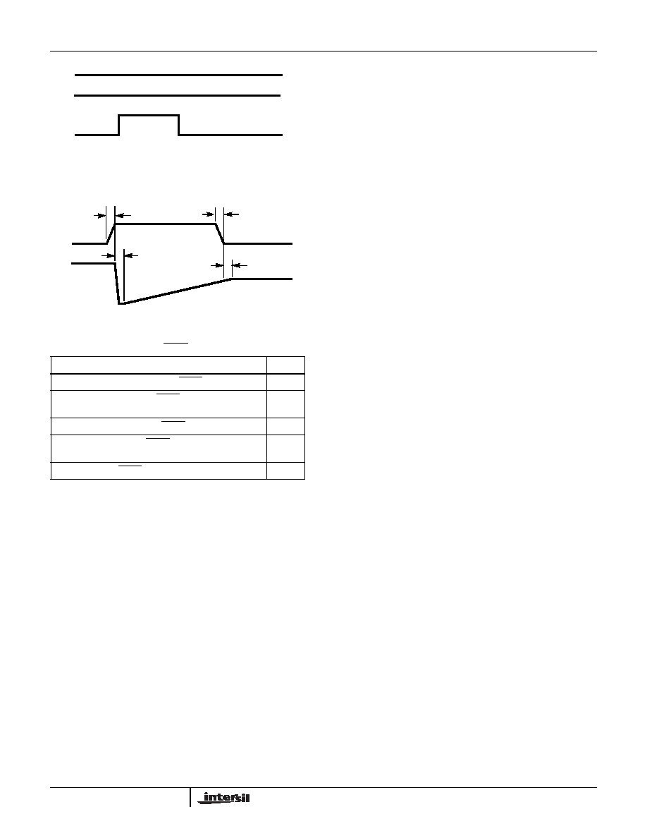
TABLE 3. SPI TIMING REQUIREMENTS
DESCRIPTION
UNITS
T1 minimum time from CS falling edge to SCK falling edge.
10ns
T2 minimum time from CS falling edge to SCK rising edge.
80ns
T3 minimum time for the SCK low.
60ns
T4 minimum time for the SCK high.
60ns
T5 minimum time from SCK rise after 8 bits to CS rising edge.
80ns
T6 minimum time from data valid to rising edge of SCK.
60ns
T7 minimum time for data valid after the rising edge of the
SCK.
10ns
T8 minimum time after CS rises until INT/HOLD goes high.
8
µ
s
B7
B6
B5
B4
B3
B2
B1
B0
DATA IN
SCK
CS
T1
T2
T3
T4
T5
T6
T7
INT/HOLD
T8
FIGURE 6. SPI TIMING
HIP9010
11
Test Multiplexer
This circuit receives the positive and negative outputs out of
the two integrators, together with the outputs from different
parts of the chip. The output is controlled by the fifth
programming word of the communications protocol. This
multiplexes the switch capacitor filter output, the gain control
output as well as the antialias output.
Differential to Single-ended Converter
This signal takes the output of the two integrators (through
the test multiplexer circuit) and provides a signal that is the
sum of the two signals. This technique is used to improve
the noise immunity of the system.
Output Buffer
This output amplifier is the same as the input amplifier used
to interface to the sensors. For test purposes when we look
at the output of the antialias filter, the input amplifiers are in
the power down mode.
TABLE 4. INTERGRATE/HOLD TIMING REQUIREMENTS
DESCRIPTION
UNITS
T1 maximum rise time of the INT/HOLD signal.
45ns
T2 maximum time after INT/HOLD rises for the INOUT to
begin to intergrate.
20
µ
s
T3 maximum fall time of INT/HOLD signal.
45ns
T4 typical time after INT/HOLD goes low before chip
goes into hold state.
20
µ
s
T5 minimum INT/HOLD time during power up sequence.
1
µ
s
CS
INT/HOLD
FIGURE 7. POWER UP SEQUENCE
INT/HOLD
INTOUT
T1
T2
T3
T4
FIGURE 8. INTEGRATOR TIMING
HIP9010
12
All Intersil U.S. products are manufactured, assembled and tested utilizing ISO9000 quality systems.
Intersil Corporation's quality certifications can be viewed at www.intersil.com/design/quality
Intersil products are sold by description only. Intersil Corporation reserves the right to make changes in circuit design, software and/or specifications at any time without
notice. Accordingly, the reader is cautioned to verify that data sheets are current before placing orders. Information furnished by Intersil is believed to be accurate and
reliable. However, no responsibility is assumed by Intersil or its subsidiaries for its use; nor for any infringements of patents or other rights of third parties which may result
from its use. No license is granted by implication or otherwise under any patent or patent rights of Intersil or its subsidiaries.
For information regarding Intersil Corporation and its products, see www.intersil.com
Sales Office Headquarters
NORTH AMERICA
Intersil Corporation
7585 Irvine Center Drive
Suite 100
Irvine, CA 92618
TEL: (949) 341-7000
FAX: (949) 341-7123
Intersil Corporation
2401 Palm Bay Rd.
Palm Bay, FL 32905
TEL: (321) 724-7000
FAX: (321) 724-7946
EUROPE
Intersil Europe Sarl
Ave. William Graisse, 3
1006 Lausanne
Switzerland
TEL: +41 21 6140560
FAX: +41 21 6140579
ASIA
Intersil Corporation
Unit 1804 18/F Guangdong Water Building
83 Austin Road
TST, Kowloon Hong Kong
TEL: +852 2723 6339
FAX: +852 2730 1433
HIP9010
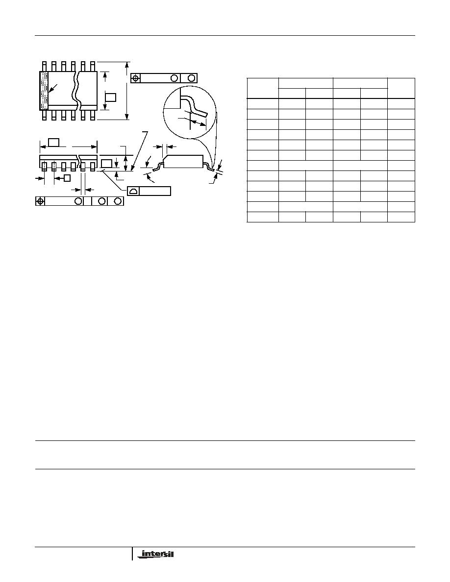
Small Outline Plastic Packages (SOIC)
NOTES:
1. Symbols are defined in the "MO Series Symbol List" in Section 2.2 of
Publication Number 95.
2. Dimensioning and tolerancing per ANSI Y14.5M-1982.
3. Dimension "D" does not include mold flash, protrusions or gate burrs.
Mold flash, protrusion and gate burrs shall not exceed 0.15mm (0.006
inch) per side.
4. Dimension "E" does not include interlead flash or protrusions. Interlead
flash and protrusions shall not exceed 0.25mm (0.010 inch) per side.
5. The chamfer on the body is optional. If it is not present, a visual index
feature must be located within the crosshatched area.
6. "L" is the length of terminal for soldering to a substrate.
7. "N" is the number of terminal positions.
8. Terminal numbers are shown for reference only.
9. The lead width "B", as measured 0.36mm (0.014 inch) or greater above
the seating plane, shall not exceed a maximum value of 0.61mm (0.024
inch)
10. Controlling dimension: MILLIMETER. Converted inch dimensions are
not necessarily exact.
INDEX
AREA
E
D
N
1
2
3
-B-
0.25(0.010)
C A
M
B S
e
-A-
L
B
M
-C-
A1
A
SEATING PLANE
0.10(0.004)
h x 45
o
C
H
µ
0.25(0.010)
B
M
M
M20.3
(JEDEC MS-013-AC ISSUE C)
20 LEAD WIDE BODY SMALL OUTLINE PLASTIC PACKAGE
SYMBOL
INCHES
MILLIMETERS
NOTES
MIN
MAX
MIN
MAX
A
0.0926
0.1043
2.35
2.65
-
A1
0.0040
0.0118
0.10
0.30
-
B
0.013
0.0200
0.33
0.51
9
C
0.0091
0.0125
0.23
0.32
-
D
0.4961
0.5118
12.60
13.00
3
E
0.2914
0.2992
7.40
7.60
4
e
0.050 BSC
1.27 BSC
-
H
0.394
0.419
10.00
10.65
-
h
0.010
0.029
0.25
0.75
5
L
0.016
0.050
0.40
1.27
6
N
20
20
7
0
o
8
o
0
o
8
o
-
Rev. 0 12/93