6-69
March 1997
HM-6508/883
1024 x 1 CMOS RAM
Features
∑ This Circuit is Processed in Accordance to
MIL-STD-883 and is Fully Conformant Under the Provi-
sions of Paragraph 1.2.1.
∑ Low Power Standby . . . . . . . . . . . . . . . . . . . . 50
µ
W Max
∑ Low Power Operation . . . . . . . . . . . . . 20mW/MHz Max
∑ Fast Access Time. . . . . . . . . . . . . . . . . . . . . . 180ns Max
∑ Data Retention . . . . . . . . . . . . . . . . . . . . . . . . . .2.0V Min
∑ TTL Compatible Input/Output
∑ High Output Drive - 2 TTL Loads
∑ On-Chip Address Register
Description
The HM-6508/883 is a 1024 x 1 static CMOS RAM
fabricated using self-aligned silicon gate technology.
Synchronous circuit design techniques are employed to
achieve high performance and low power operation.
On chip latches are provided for address allowing efficient
interfacing with microprocessor systems. The data output
buffers can be forced to a high impedance state for use in
expanded memory arrays.
The HM-6508/883 is a fully static RAM and may be main-
tained in any state for an indefinite period of time. Data
retention supply voltage and supply current are guaranteed
over temperature.
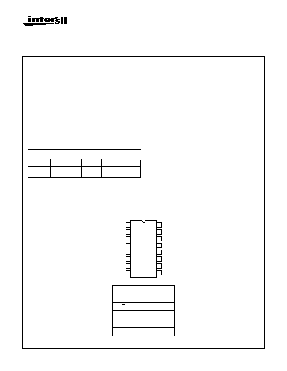
Pinout
HM1-6508/883
(CERDIP)
TOP VIEW
Ordering Information
PACKAGE
TEMP. RANGE
180ns
250ns
PKG. NO.
CERDIP
-55
o
C to +125
o
C HM1-
6508B/883
HM1-
6508/883
F16.3
PIN
DESCRIPTION
A
Address Input
E
Chip Enable
W
Write Enable
D
Data Input
Q
Data Output
14
15
16
9
13
12
11
10
1
2
3
4
5
7
6
8
E
A0
A1
A2
A3
A4
GND
Q
VCC
W
A9
A8
A7
A6
A5
D
File Number
2985.1
CAUTION: These devices are sensitive to electrostatic discharge; follow proper IC Handling Procedures.
http://www.intersil.com or 407-727-9207
|
Copyright
©
Intersil Corporation 1999

6-70
Functional Diagram
NOTES:
1. All lines positive logic - active high.
2. Three-state buffers: A high
output active.
3. Address latches and gated decoders: Latch on falling edge of E and gate on falling edge of E.
5
A
LATCHED ADDRESS
REGISTER
LATCHED
ADDRESS
REGISTER
GATED
ROW
DECODER
32
GATED COLUMN
DECODER
AND DATA I/O
E
W
Q
A5
A4
A3
A2
A1
A0
32 x 32
MATRIX
5
5
A
A
32
5
A
A6
A7
A8
A9
D
A
A
HM-6508/883

6-71
Absolute Maximum Ratings
Thermal Information
Supply Voltage . . . . . . . . . . . . . . . . . . . . . . . . . . . . . . . . . . . . . +7.0V
Input, Output or I/O Voltage . . . . . . . . . . . GND -0.3V to VCC +0.3V
Typical Derating Factor . . . . . . . . . . .1.5mA/MHz Increase in ICCOP
ESD Classification . . . . . . . . . . . . . . . . . . . . . . . . . . . . . . . . Class 1
Operating Conditions
Operating Voltage Range . . . . . . . . . . . . . . . . . . . . . +4.5V to +5.5V
Operating Temperature Range . . . . . . . . . . . . . . . . -55
o
C to +125
o
C
Input Low Voltage . . . . . . . . . . . . . . . . . . . . . . . . . . . . . . 0V to +0.8V
Input High Voltage . . . . . . . . . . . . . . . . . . . . . . . .VCC -2.0V to VCC
Input Rise and Fall Time. . . . . . . . . . . . . . . . . . . . . . . . . . 40ns Max.
Thermal Resistance (Typical, Note 1)
JA
JC
CERDIP Package . . . . . . . . . . . . . . . .
75
o
C/W
15
o
C/W
Maximum Storage Temperature Range . . . . . . . . .-65
o
C to +150
o
C
Maximum Junction Temperature . . . . . . . . . . . . . . . . . . . . . . +175
o
C
Maximum Lead Temperature (Soldering 10s) . . . . . . . . . . . . +300
o
C
Die Characteristics
Gate Count . . . . . . . . . . . . . . . . . . . . . . . . . . . . . . . . . . . 1925 Gates
CAUTION: Stresses above those listed in "Absolute Maximum Ratings" may cause permanent damage to the device. This is a stress only rating and operation
of the device at these or any other conditions above those indicated in the operational sections of this specification is not implied.
NOTE:
1.
JA
is measured with the component mounted on an evaluation PC board in free air.
TABLE 1. HM-6508/883 DC ELECTRICAL PERFORMANCE SPECIFICATIONS
Device Guaranteed and 100% Tested
PARAMETER
SYMBOL
(NOTE 1)
CONDITIONS
GROUP A
SUBGROUPS
TEMPERATURE
LIMITS
UNITS
MIN
MAX
Output Low Voltage
VOL
VCC = 4.5V,
IOL = 3.2mA
1, 2, 3
-55
o
C
T
A
+125
o
C
-
0.4
V
Output High Voltage
VOH
VCC = 4.5V,
IOH = -0.4mA
1, 2, 3
-55
o
C
T
A
+125
o
C
2.4
-
V
Input Leakage Current
II
VCC = 5.5V,
VI = GND or VCC
1, 2, 3
-55
o
C
T
A
+125
o
C
-1.0
+1.0
µ
A
Output Leakage Current
IOZ
VCC = 5.5V,
VO = GND or VCC
1, 2, 3
-55
o
C
T
A
+125
o
C
-1.0
+1.0
µ
A
Data Retention Supply Current
ICCDR
VCC = 2.0V,
E = VCC,
IO = 0mA,
VI = VCC or GND
1, 2, 3
-55
o
C
T
A
+125
o
C
-
5
µ
A
HM-6508B/883
HM-6508/883
-
10
µ
A
Operating Supply Current
ICCOP
VCC = 5.5V,
(Note 2),
E = 1MHz,
IO = 0mA,
1, 2, 3
-55
o
C
T
A
+125
o
C
-
4
mA
Standby Supply Current
ICCSB
VCC = 5.0V,
IO = 0mA,
VI = VCC or GND
1, 2, 3
-55
o
C
T
A
+125
o
C
-
10
µ
A
NOTES:
1. All voltages referenced to device GND.
2. Typical derating 1.5mA/MHz increase in ICCOP.
HM-6508/883

6-72
TABLE 2. HM-6508/883 AC ELECTRICAL PERFORMANCE SPECIFICATIONS
Device Guaranteed and 100% Tested
PARAMETER
SYMBOL
(NOTES 1, 2)
CONDITIONS
GROUP A
SUB-
GROUPS
TEMPERATURE
LIMITS
UNITS
HM-6508B/883
HM-6508/883
MIN
MAX
MIN
MAX
Chip Enable
Access Time
(1) TELQV
VCC = 4.5 and
5.5V
9, 10, 11
-55
o
C
T
A
+125
o
C
-
180
-
250
ns
Address Access
Time
(2) TAVQV
VCC = 4.5 and
5.5V, Note 3
9, 10, 11
-55
o
C
T
A
+125
o
C
-
180
-
250
ns
Chip Enable
Output Disable
Time
(3) TELQX
VCC = 4.5 and
5.5V
9, 10, 11
-55
o
C
T
A
+125
o
C
5
-
5
-
ns
Write Enable
Output Disable
Time
(4) TWLQZ
VCC = 4.5 and
5.5V
9, 10, 11
-55
o
C
T
A
+125
o
C
-
120
-
160
ns
Chip Enable
Output Disable
Time
(5) TEHQZ
VCC = 4.5 and
5.5V
9, 10, 11
-55
o
C
T
A
+125
o
C
-
120
-
160
ns
Chip Enable
Pulse Negative
Width
(6) TELEH
VCC = 4.5 and
5.5V
9, 10, 11
-55
o
C
T
A
+125
o
C
180
-
250
-
ns
Chip Enable
Pulse Positive
Width
(7) TEHEL
VCC = 4.5 and
5.5V
9, 10, 11
-55
o
C
T
A
+125
o
C
100
-
100
-
ns
Address Setup
Time
(8) TAVEL
VCC = 4.5 and
5.5V
9, 10, 11
-55
o
C
T
A
+125
o
C
0
-
0
-
ns
Address Hold
Time
(9) TELAX
VCC = 4.5 and
5.5V
9, 10, 11
-55
o
C
T
A
+125
o
C
40
-
50
-
ns
Data Setup Time
(10) TDVWH
VCC = 4.5 and
5.5V
9, 10, 11
-55
o
C
T
A
+125
o
C
80
-
110
-
ns
Data Hold Time
(11) TWHDX
VCC = 4.5 and
5.5V
9, 10, 11
-55
o
C
T
A
+125
o
C
0
-
0
-
ns
Chip Enable
Write Pulse
Setup Time
(12) TWLEH
VCC = 4.5 and
5.5V
9, 10, 11
-55
o
C
T
A
+125
o
C
100
-
130
-
ns
Chip Enable
Write Pulse Hold
Time
(13) TELWH
VCC = 4.5 and
5.5V
9, 10, 11
-55
o
C
T
A
+125
o
C
100
-
130
-
ns
Write Enable
Pulse Width
(14) TWLWH
VCC = 4.5 and
5.5V
9, 10, 11
-55
o
C
T
A
+125
o
C
100
-
130
-
ns
Read or Write
Cycle Time
(15) TELEL
VCC = 4.5 and
5.5V
9, 10, 11
-55
o
C
T
A
+125
o
C
280
-
350
-
ns
NOTES:
1. All voltages referenced to device GND.
2. Input pulse levels: 0.8V to VCC -2.0V; Input rise and fall times: 5ns (max); input and output timing reference level: 1.5V; Output load:
1TTL gate equivalent, CL = 50pF (min) - for CL greater than 50pF, access time is derated by 0.15ns per pF.
3. TAVQV = TELQV + TAVEL.
HM-6508/883

6-73
Timing Waveforms
TABLE 3. HM-6508/883 ELECTRICAL PERFORMANCE SPECIFICATIONS
PARAMETER
SYMBOL
CONDITIONS
NOTE
TEMPERATURE
LIMITS
UNITS
MIN
MAX
Input Capacitance
CI
VCC = Open, f = 1MHz, All
Measurements Referenced
to Device Ground
1
T
A
= +25
o
C
-
6
pF
Output Capacitance
CO
VCC = Open, f = 1MHz, All
Measurements Referenced
to Device Ground
1
T
A
= +25
o
C
-
10
pF
NOTE:
1. The parameters listed in Table 3 are controlled via design or process; parameters are characterized upon initial design and after major
process and/or design changes.
TABLE 4. APPLICABLE SUBGROUPS
CONFORMANCE GROUPS
METHOD
SUBGROUPS
Initial Test
100%/5004
-
Interim Test
100%/5004
1, 7, 9
PDA
100%/5004
1
Final Test
100%/5004
2, 3, 8A, 8B, 10, 11
Group A
Samples/5005
1, 2, 3, 7, 8A, 8B, 9, 10, 11
Groups C & D
Samples/5005
1, 7, 9
(8)
-1
TIME
HIGH
TAVEL
VALID
TELAX
(8) TAVEL
TELEL
TELEH
VALID OUTPUT
(5)
(7)
TEHEL
(6)
(9)
(15)
(7)
NEXT
TEHEL
TEHOZ
TELOV
(5)
(1)
(3)
(3)
TELOX
TAVQV
TEHOZ
0
1
2
3
4
5
REFERENCE
A
E
W
D
O
FIGURE 1. READ CYCLE
HM-6508/883

6-74
In the HM-6508/883 Read Cycle, the address information is
latched into the on-chip registers on the falling edge of E
(T = 0). Minimum address setup and hold time requirements
must be met. After the required hold time, the addresses
may change state without affecting device operation. During
time (T = 1) the data output becomes enabled; however, the
data is not valid until during time (T = 2).
W must remain high for the read cycle. After the output data
has been read, E may return high (T = 3). This will disable
the chip and force the output buffer to a high impedance
state. After the required E high time (TEHEL) the RAM is
ready for the next memory cycle (T = 4).
Timing Wavforms
(continued)
TRUTH TABLE
TIME REFERENCE
INPUTS
OUTPUTS
FUNCTION
E
W
A
D
Q
-1
H
X
X
X
Z
Memory Disabled
0
H
V
X
Z
Cycle Begins, Addresses are Latched
1
L
H
X
X
X
Output Enabled
2
L
H
X
X
V
Output Valid
3
H
X
X
V
Read Accomplished
4
H
X
X
X
Z
Prepare for Next Cycle (Same as -1)
5
H
V
X
Z
Cycle Ends, Next Cycle Begins (Same as 0)
TIME
REFERENCE
(8) TAVEL
TELAX
(9)
(8) TAVEL
NEXT
TELEL
TEHEL
(15)
(7)
TELEH
(6)
(7)
TEHEL
TWLEH
(14)
(12)
TWLWH
(13)
VALID DATA INPUT
TELWH
TWHDX (11)
TDVWH
(10)
HIGH 2
-1
0
1
2
3
4
5
A
E
W
D
O
VALID
FIGURE 2. WRITE CYCLE
HM-6508/883

6-75
The write cycle is initiated by the falling edge of E which
latches the address information into the on chip registers.
The write portion of the cycle is defined as both E and W
being low simultaneously. W may go low anytime during the
cycle, provided that the write enable pulse setup time
(TWLEH) is met. The write portion of the cycle is terminated
by the first rising edge of either E or W. Data setup and hold
times must be referenced to the terminating signal.
If a series of consecutive write cycles are to be performed,
the W line may remain low until all desired locations have
been written. When this method is used, data setup and hold
times must be referenced to the rising edge of E. By posi-
tioning the W pulse at different times within the E low time
(TELEH), various types of write cycles may be performed.
If the E low time (TELEH) is greater than the W pulse
(TWLWH), plus an output enable time (TELQX), a combina-
tion read write cycle is executed. Data may be modified an
indefinite number of times during any write cycle (TELEH).
The data input and data output pins may be tied together for
use with a common I/O data bus structure. When using the
RAM in this method, allow a minimum of one output disable
time (TWLQZ) after W goes low before applying input data to
the bus. This will ensure that the output buffers are not active.
Test Load Circuit
NOTE:
1. Test head capacitance includes stray and jig capacitance.
TRUTH TABLE
TIME
REFERENCE
INPUTS
OUTPUTS
FUNCTION
E
W
A
D
Q
-1
H
X
X
X
Z
Memory Disabled
0
X
V
X
Z
Cycle Begins, Addresses are Latched
1
L
X
X
Z
Write Period Begins
2
L
X
V
Z
Data is Written
3
H
X
X
Z
Write Completed
4
H
X
X
X
Z
Prepare for Next Cycle (Same as -1)
5
X
V
X
Z
Cycle Ends, Next Cycle Begins (Same as 0)
DUT
1.5V
IOL
IOH
+
-
(NOTE 1) CL
EQUIVALENT CIRCUIT
HM-6508/883

6-76
Burn-In Circuit
HM6508/883 CERDIP
NOTES:
1. All resistors 47k
±
5%.
2. F0 = 100kHz
±
10%.
3. F1 = F0
˜
2, F2 = F1
˜
2, F3 = F2
˜
2. . . F12 = F11
˜
2.
4. VCC = 5.5V
±
0.5V.
5. VIH = 4.5V
±
10%.
6. VIL = -0.2V to +0.4V.
7. C1 = 0.01
µ
F Min.
14
15
16
9
13
12
11
10
1
2
3
4
5
7
6
8
A0
A1
A2
A3
A4
GND
Q
E
VCC
A9
A8
A7
A6
A5
D
W
C1
VCC
F2
F1
F12
F11
F8
F0
F7
F6
F4
F2
F3
F5
F10
F9
HM-6508/883
6-77
All Intersil semiconductor products are manufactured, assembled and tested under ISO9000 quality systems certification.
Intersil products are sold by description only. Intersil Corporation reserves the right to make changes in circuit design and/or specifications at any time without
notice. Accordingly, the reader is cautioned to verify that data sheets are current before placing orders. Information furnished by Intersil is believed to be accurate
and reliable. However, no responsibility is assumed by Intersil or its subsidiaries for its use; nor for any infringements of patents or other rights of third parties which
may result from its use. No license is granted by implication or otherwise under any patent or patent rights of Intersil or its subsidiaries.
For information regarding Intersil Corporation and its products, see web site http://www.intersil.com
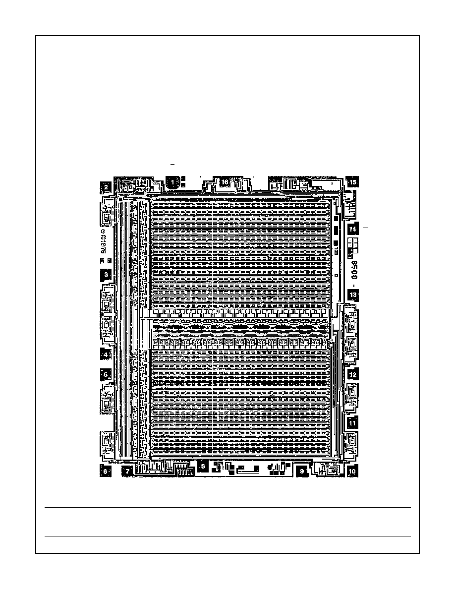
Die Characteristics
DIE DIMENSIONS:
130 x 150 x 19
±
1mils
METALLIZATION:
Type: Si - Al
Thickness: 11k
≈
±
2k
≈
GLASSIVATION:
Type: SiO
2
Thickness: 8k
≈
±
1k
≈
WORST CASE CURRENT DENSITY:
1.342 x 10
5
A/cm
2
LEAD TEMPERATURE (10s soldering):
300
o
C
Metallization Mask Layout
HM-6508/883
VCC
E
A0
A1
A2
A3
A4
Q
GND
A5
A7
A8
A9
W
D
A6
HM-6508/883