6-101
March 1997
HM-6551/883
256 x 4 CMOS RAM
Features
∑ This Circuit is Processed in Accordance to MIL-STD-
883 and is Fully Conformant Under the Provisions of
Paragraph 1.2.1.
∑ Low Power Standby . . . . . . . . . . . . . . . . . . . . 50
µ
W Max
∑ Low Power Operation . . . . . . . . . . . . . 20mW/MHz Max
∑ Fast Access Time. . . . . . . . . . . . . . . . . . . . . . 220ns Max
∑ Data Retention . . . . . . . . . . . . . . . . . . . . . . . .at 2.0V Min
∑ TTL Compatible Input/Output
∑ High Output Drive - 1 TTL Load
∑ Internal Latched Chip Select
∑ High Noise Immunity
∑ On-Chip Address Register
∑ Latched Outputs
∑ Three-State Output
Description
The HM-6551/883 is a 256 x 4 static CMOS RAM fabricated
using self-aligned silicon gate technology. Synchronous cir-
cuit design techniques are employed to achieve high perfor-
mance and low power operation. On chip latches are
provided for address and data outputs allowing efficient
interfacing with microprocessor systems. The data output
buffers can be forced to a high impedance state for use in
expanded memory arrays.
The HM-6551/883 is a fully static RAM and may be main-
tained in any state for an indefinite period of time. Data
retention supply voltage and supply current are guaranteed
over temperature.
Ordering Information
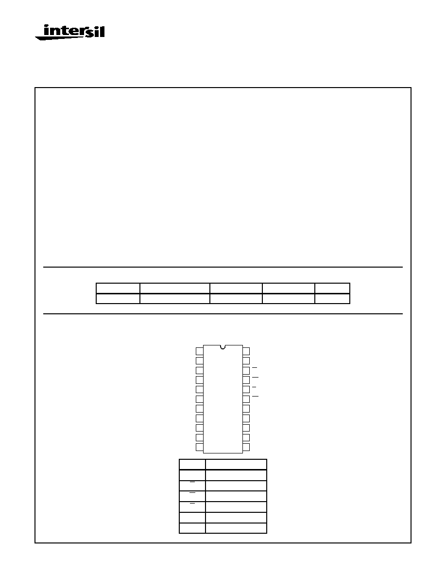
Pinout
HM-6551/883 (CERDIP)
TOP VIEW
PACKAGE
TEMPERATURE RANGE
220ns
300ns
PKG. NO.
CERDIP
-55
o
C to +125
o
C
HM-6551B/883
HM1-6551/883
F22.4
PIN
DESCRIPTION
A
Address Input
E
Chip Enable
W
Write Enable
S
Chip Select
D
Data Input
Q
Data Output
1
22
12
13
14
15
16
17
18
19
21
20
11
10
9
8
7
6
5
3
2
A2
A1
A0
A5
A6
A7
D0
GND
Q0
D1
A4
Q3
D3
Q2
D2
Q1
4
A3
VCC
W
S1
E
S2
File Number
2988.1
CAUTION: These devices are sensitive to electrostatic discharge; follow proper IC Handling Procedures.
http://www.intersil.com or 407-727-9207
|
Copyright
©
Intersil Corporation 1999
6-102
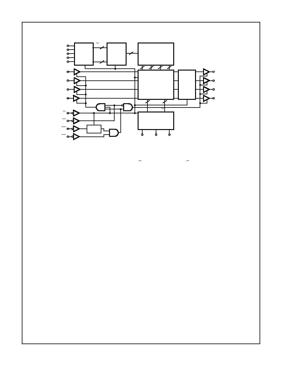
Functional Diagram
NOTES:
1. Select Latch: L Low
Q = D and Q latches on rising edge of L.
2. Address Latches And Gated Decoders: Latch on falling edge of E and gate on falling edge of E.
3. All lines positive logic-active high.
4. Three-State Buffers: A high
output active.
5. Data Latches: L High
Q = D and Q latches on falling edge of L.
GATED
ROW
DECODER
A0
32
5
5
A
A1
A5
A6
A7
A
LATCHED
ADDRESS
REGISTER
32 x 32
MATRIX
D
3
3
A
A
S1
S2
W
E
LATCH
SELECT
A4
A3
A2
LATCHED ADDRESS
REGISTER
LATCHES
DATA
OUTPUT
GATED COLUMN
DECODER
AND DATA I/O
D0
A
A
A
A
A
A
A
A
L
8
8
8
8
D
D
D
D1
D2
D3
D
Q
L
Q
Q
Q
Q
Q0
Q1
Q2
Q3
HM-6551/883
6-103
Absolute Maximum Ratings
Thermal Information
Supply Voltage . . . . . . . . . . . . . . . . . . . . . . . . . . . . . . . . . . . . . +7.0V
Input, Output or I/O Voltage . . . . . . . . . . . GND -0.3V to VCC +0.3V
ESD Classification . . . . . . . . . . . . . . . . . . . . . . . . . . . . . . . . Class 1
Thermal Resistance
JA
JC
CERDIP Package . . . . . . . . . . . . . . . .
60
o
C/W
15
o
C/W
Maximum Storage Temperature Range . . . . . . . . .-65
o
C to +150
o
C
Maximum Junction Temperature . . . . . . . . . . . . . . . . . . . . . . +175
o
C
Maximum Lead Temperature (Soldering 10s) . . . . . . . . . . . . +300
o
C
Die Characteristics
Gate Count . . . . . . . . . . . . . . . . . . . . . . . . . . . . . . . . . . . 1930 Gates
CAUTION: Stresses above those listed in "Absolute Maximum Ratings" may cause permanent damage to the device. This is a stress only rating and operation
of the device at these or any other conditions above those indicated in the operational sections of this specification is not implied.
Operating Conditions
Operating Voltage Range . . . . . . . . . . . . . . . . . . . . . +4.5V to +5.5V
Operating Temperature Range . . . . . . . . . . . . . . . . -55
o
C to +125
o
C
Input Low Voltage . . . . . . . . . . . . . . . . . . . . . . . . . . . . . . 0V to +0.8V
Input High Voltage . . . . . . . . . . . . . . . . . . . . . . . . VCC -2.0V to VCC
Input Rise and Fall Time . . . . . . . . . . . . . . . . . . . . . . . . . . 40ns Max.
TABLE 1. HM-6551/883 DC ELECTRICAL PERFORMANCE SPECIFICATIONS
Device Guaranteed and 100% Tested
PARAMETER
SYMBOL
(NOTE 1)
CONDITIONS
GROUP A
SUBGROUPS
TEMPERATURE
LIMITS
UNITS
MIN
MAX
Output Low Voltage
VOL
VCC = 4.5V
IOL = 1.6mA
1, 2, 3
-55
o
C
T
A
+125
o
C
-
0.4
V
Output High Voltage
VOH
VCC = 4.5V
IOH = -0.4mA
1, 2, 3
-55
o
C
T
A
+125
o
C
2.4
-
V
Input Leakage Current
II
VCC = 5.5V,
VI = GND or VCC
1, 2, 3
-55
o
C
T
A
+125
o
C
-1.0
+1.0
µ
A
Output Leakage
Current
IOZ
VCC = 5.5 V,
VO = GND or VCC
1, 2, 3
-55
o
C
T
A
+125
o
C
-1.0
+1.0
µ
A
Data Retention Supply
Current
ICCDR
VCC = 2.0V, E = VCC
IO = 0mA,
VI = VCC or GND
1, 2, 3
-55
o
C
T
A
+125
o
C
-
10
µ
A
Operating Supply
Current
ICCOP
VCC = 5.5V, (Note 2)
E = 1MHz, IO = 0mA
VI = VCC or GND
1, 2, 3
-55
o
C
T
A
+125
o
C
-
4
mA
Standby Supply
Current
ICCSB
VCC = 5.5V,
IO = 0mA
VI = VCC or GND
1, 2, 3
-55
o
C
T
A
+125
o
C
-
10
µ
A
NOTES:
1. All voltages referenced to device GND.
2. Typical derating 1.5mA/MHz increase in ICCOP.
HM-6551/883
6-104
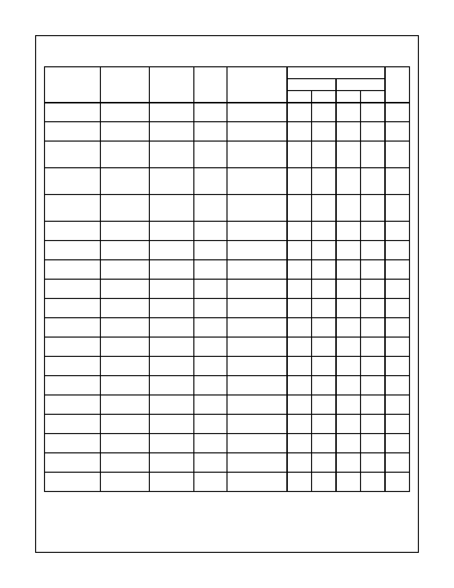
TABLE 2. HM-6551/883 A.C. ELECTRICAL PERFORMANCE SPECIFICATIONS
Device Guaranteed and 100% Tested
PARAMETER
SYMBOL
(NOTES 1, 2)
CONDITIONS
GROUP A
SUB-
GROUPS
TEMPERATURE
LIMITS
UNITS
HM-6551B/883
HM-6551/883
MIN
MAX
MIN
MAX
Chip Enable
Access Time
(1)
TELQV
VCC = 4.5 and
5.5V
9, 10, 11
-55
o
C
T
A
+125
o
C
-
220
-
300
ns
Address Access
Time
(2)
TAVQV
VCC = 4.5 and
5.5V, Note 3
9, 10, 11
-55
o
C
T
A
+125
o
C
-
220
-
300
ns
Chip Select 1
Output Enable
Time
(3)
TS1LQX
VCC = 4.5 and
5.5V
9, 10, 11
-55
o
C
T
A
+125
o
C
5
-
5
-
ns
Write Enable
Output Disable
Time
(4)
TWLQZ
VCC = 4.5 and
5.5V
9, 10, 11
-55
o
C
T
A
+125
o
C
-
130
-
150
ns
Chip Select 1
Output Disable
Time
(5)
TS1HQZ
VCC = 4.5 and
5.5V
9, 10, 11
-55
o
C
T
A
+125
o
C
-
130
-
150
ns
Chip Enable Pulse
Negative Width
(6)
TELEH
VCC = 4.5 and
5.5V
9, 10, 11
-55
o
C
T
A
+125
o
C
220
-
300
-
ns
Chip Enable Pulse
Positive Width
(7)
TEHEL
VCC = 4.5 and
5.5V
9, 10, 11
-55
o
C
T
A
+125
o
C
100
-
100
-
ns
Address Setup
Time
(8)
TAVEL
VCC = 4.5 and
5.5V
9, 10, 11
-55
o
C
T
A
+125
o
C
0
-
0
-
ns
Chip Select 2
Setup Time
(9)
TS2LEL
VCC = 4.5 and
5.5V
9, 10, 11
-55
o
C
T
A
+125
o
C
0
-
0
-
ns
Address Hold Time
(10)
TELAX
VCC = 4.5 and
5.5V
9, 10, 11
-55
o
C
T
A
+125
o
C
40
-
50
-
ns
Chip Select 2 Hold
Time
(11)
TELS2X
VCC = 4.5 and
5.5V
9, 10, 11
-55
o
C
T
A
+125
o
C
40
-
50
-
ns
Data Setup Time
(12)
TDVWH
VCC = 4.5 and
5.5V
9, 10, 11
-55
o
C
T
A
+125
o
C
100
-
150
-
ns
Data Hold Time
(13)
TWHDX
VCC = 4.5 and
5.5V
9, 10, 11
-55
o
C
T
A
+125
o
C
0
-
0
-
ns
Chip Select 1 Write
Pulse Setup Time
(14)
TWLS1H
VCC = 4.5 and
5.5V
9, 10, 11
-55
o
C
T
A
+125
o
C
120
-
180
-
ns
Chip Enable Write
Pulse Setup Time
(15)
TWLEH
VCC = 4.5 and
5.5V
9, 10, 11
-55
o
C
T
A
+125
o
C
120
-
180
-
ns
Chip Select 1 Write
Pulse Hold Time
(16)
TS1LWH
VCC = 4.5 and
5.5V
9, 10, 11
-55
o
C
T
A
+125
o
C
120
-
180
-
ns
Chip Enable Write
Pulse Hold Time
(17)
TELWH
VCC = 4.5 and
5.5V
9, 10, 11
-55
o
C
T
A
+125
o
C
120
-
180
-
ns
Write Enable Pulse
Width
(18)
TWLWH
VCC = 4.5 and
5.5V
9, 10, 11
-55
o
C
T
A
+125
o
C
120
-
180
-
ns
Read or Write
Cycle Time
(19)
TELEL
VCC = 4.5 and
5.5V
9, 10, 11
-55
o
C
T
A
+125
o
C
320
-
400
-
ns
NOTES:
1. All voltages referenced to device GND.
2. Input pulse levels: 0.8V to VCC-2.0V; Input rise and fall times: 5ns (max); Input and output timing reference level: 1.5V; Output load:
IOL = 1.6mA, IOH = -0.4mA, CL = 50pF (min) - for CL greater than 50pF, access time is derated by 0.15ns per pF.
3. TAVQV = TELQV + TAVEL.
HM-6551/883
6-105
TABLE 3. HM-6551B/883 AND HM-6551/883 ELECTRICAL PERFORMANCE SPECIFICATIONS
PARAMETER
SYMBOL
CONDITIONS
NOTE
TEMPERATURE
LIMITS
UNITS
MIN
MAX
Input Capacitance
CI
VCC = Open, f = 1MHz, All
Measurements Referenced to
Device Ground
1
T
A
= +25
o
C
-
10
pF
Output Capacitance
CO
VCC = Open, f = 1MHz, All
Measurements Referenced to
Device Ground
1
T
A
= +25
o
C
-
12
pF
NOTE:
1. The parameters listed in Table 3 are controlled via design or process parameters are characterized upon initial design and after major
process and/or design changes.
TABLE 4. APPLICABLE SUBGROUPS
CONFORMANCE GROUPS
METHOD
SUBGROUPS
Initial Test
100%/5004
-
Interim Test
100%/5004
1, 7, 9
PDA
100%/5004
1
Final Test
100%/5004
2, 3, 8A, 8B, 10, 11
Group A
Samples/5005
1, 2, 3, 7, 8A, 8B, 9, 10, 11
Groups C & D
Samples/5005
1, 7, 9
HM-6551/883