1
Semiconductor
March 1998
HMP8112A
NTSC/PAL Video Decoder
Features
∑ Supports ITU-R BT.601 (CCIR601) and Square Pixel
∑ 3 Composite Analog Inputs with Sync Tip AGC, Black
Clamping and White Peak Control
∑ Patented Decoding Scheme with Improved 2-Line
Comb Filter, Y/C Separation
∑ NTSC M and PAL (B, D, G, H, I, M, N, CN) Operation
∑ Composite or S-Video Input
∑ User-Selectable Color Trap and Low Pass Video
Filters
∑ User Selectable Hue, Saturation, Contrast, Sharpness,
and Brightness Controls
∑ User Selectable Data Transfer Output Modes
∑ 16-Bit 4:2:2 YCbCr
∑ 8-Bit 4:2:2 YCbCr
∑ User Selectable Clock Range from 20MHz - 30MHz
∑ I
2
C Interface
∑ VMI Compatible Video Data Bus
Applications
∑ Multimedia PCs
∑ Video Conferencing
∑ Video Editing
∑ Video Security Systems
∑ Digital VCRs
∑ Related Products
- NTSC/PAL Encoders: HMP8154, HMP8156A,
HMP8170/1, HMP8172/3
- NTSC/PAL Decoders: HMP8115, HMP8130/1
Description
The HMP8112A is a high quality, digital video, color decoder
with internal A/D converters. The A/D function includes a 3:1
analog input mux, Sync Tip AGC, Black clamping and two 8-
bit A/D Converters. The high quality A/D converters minimize
pixel jitter and crosstalk.
The decoder function is compatible with NTSC M, PAL B, D,
G, H, I, M, N and special combination PAL N video stan-
dards. Both composite (CVBS) and S-Video (Y/C) input for-
mats are supported. A 2-line comb filter plus a user
selectable Chrominance trap filter provide high quality Y/C
separation. Various adjustments are available to optimize
the image such as Brightness, Contrast, Saturation, Hue and
Sharpness controls. Video synchronization is achieved with
a 4xf
SC
chroma burst lock PLL for color demodulation and
line lock PLL for correct pixel alignment. A chrominance sub-
sampling 4:2:2 scheme is provided to reduce chrominance
bandwidth.
The HMP8112A is ideally suited as the analog video inter-
face to VCR's and camera's in any multimedia or video sys-
tem. The high quality Y/C separation, user flexibility and
integrated phase locked loops are ideal for use with today's
powerful compression processors. The HMP8112A operates
from a single 5V supply and is TTL/CMOS compatible.
Table of Contents
Page
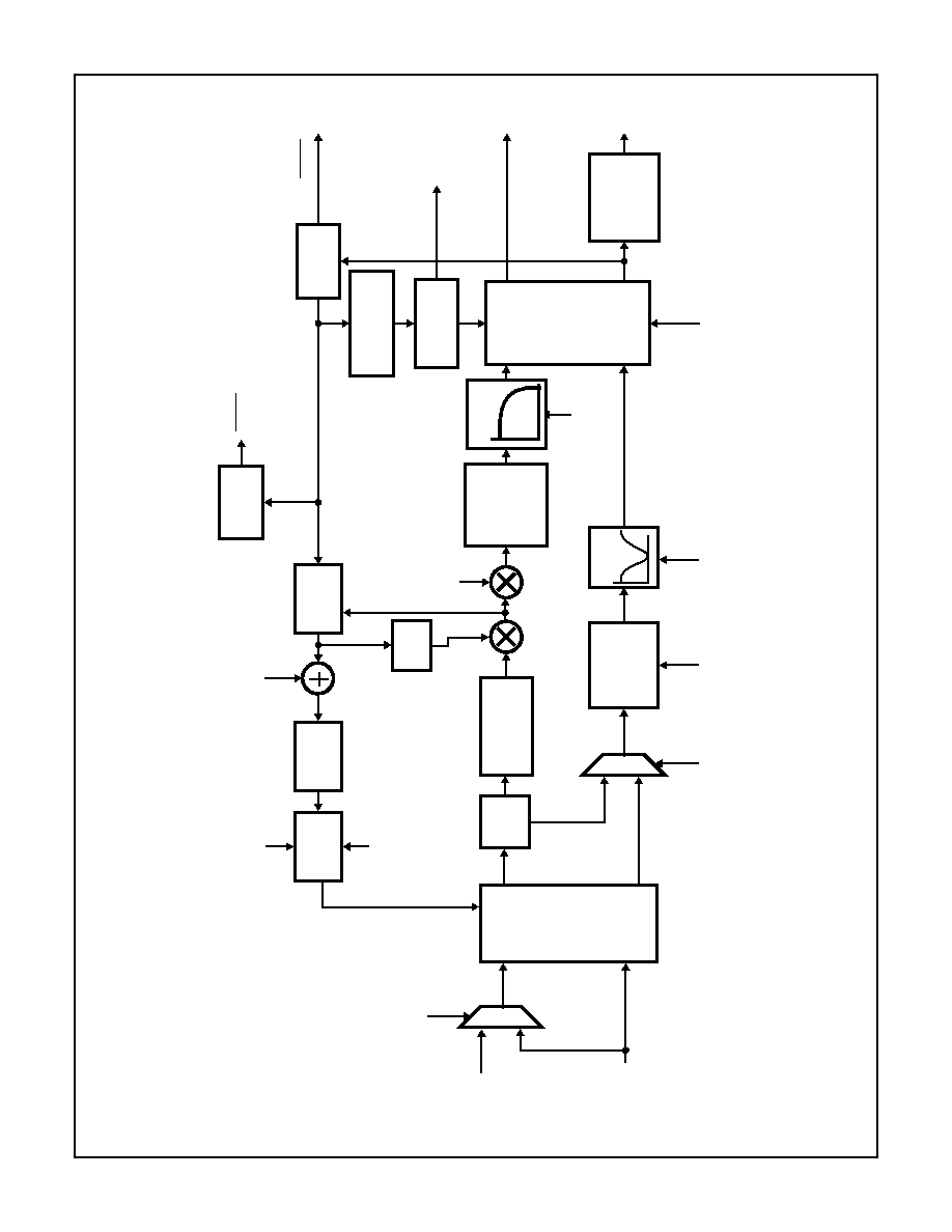
Functional Block Diagrams . . . . . . . . . . . . . . . . . . . . . . . . 2
Functional Operation Introduction. . . . . . . . . . . . . . . . . . . 5
Internal Register Description Tables . . . . . . . . . . . . . . . . 15
Pinout . . . . . . . . . . . . . . . . . . . . . . . . . . . . . . . . . . . . . . . 22
Pin Descriptions . . . . . . . . . . . . . . . . . . . . . . . . . . . . . . . 23
AC and DC Electrical Specifications . . . . . . . . . . . . . . . . 25
Typical Performance Curves . . . . . . . . . . . . . . . . . . . . . . 28
Applications Information . . . . . . . . . . . . . . . . . . . . . . . . . 39
Package Dimensions . . . . . . . . . . . . . . . . . . . . . . . . . . . 40
Ordering Information
PART NUMBER
TEMP.
RANGE (
o
C)
PACKAGE
PKG.NO.
HMP8112ACN
0 to 70
80 Ld PQFP
Q80.14x20
HMP8112EVAL2
PCI Reference Design (Includes Part)
HMP8156EVAL2
Frame Grabber Evaluation Board
(Includes Part)
PQFP is also known as QFP and MQFP
CAUTION: These devices are sensitive to electrostatic discharge. Users should follow proper IC Handling Procedures.
Copyright
©
Harris Corporation 1998
File Number
4407.2
NOT RECOMMENDED FOR NEW DESIGNS
See HMP8115

5
Introduction
The HMP8112A is designed to decode baseband composite
or s-video NTSC and PAL signals, and convert them to either
digital YCbCr or RGB data.
The digital PLLs are designed to synchronize to all NTSC
and PAL standards. A chroma PLL is used to maintain
chroma lock for demodulation of the color information; a line-
locked PLL is used to maintain vertical spatial alignment.
The PLLs are designed to maintain lock even in the event of
VCR headswitches.
The HMP8112A contains two 8-bit A/D converters and an
I
2
C port for programming internal registers
Analog Video Inputs
The HMP8112A supports either three composite or two
composite and one S-Video input.
Three analog video inputs (LIN0, LIN1, LIN2) are used to
select which one of three composite video sources are to be
decoded. To support S-video applications, the Y channel
drives the LIN2 analog input, and the C channel drives the
CIN analog input.
The analog inputs must be AC-coupled to the video signals,
as shown in the Applications section.
Anti-Aliasing Filter
An external anti-alias filter is required to achieve optimum
performance and prevent high frequency components from
being aliased back into the video image.
For the LIN0-2 inputs, a single filter is connected to L_OUT
and L_ADIN. For CIN the anti-aliasing filter should be con-
nected to the CIN input. A recommended filter is shown
below in Figure 1.
Luminance AGC And DC RESTORE Circuits
After a
RESET
, a change of the video standard, or a PLL
Chrominance Subcarrier Ratio Register load, the decoder
enters Acquisition Mode by attempting to lock to a new video
source. During this mode, the HAGC and DC RESTORE cir-
cuits perform continuous gain and bias adjustments until the
PLL is LOCKED onto the video signal. Once LOCKED, the
HAGC and DC RESTORE functions are performed during
programmable window periods for each horizontal video line.
The digital PLL zeroes a 10-bit pixel clock counter during
each horizontal sync tip and increments the count for each
pixel of the entire video line. The AGC amplifier attenuates or
amplifies the analog video signal during the horizontal sync
tip to maintain an average ADC code of 0. The DC
RESTORE circuit clamps the video signal during the back
porch to maintain an average ADC code of 64. Reference
Figure 2 for timing information and Table 5 for the recom-
mended register values to use for different video standards.
The START and END times of the HSYNC output are also
programmable and can be used as a reference for confirm-
ing proper HAGC and DC RESTORE timing.
White Peak Enable
The white peak enable input, (WPE) enables or disables the
white peak control of the luminance input. If enabled, the
AGC will reduce the gain of the video amplifier when the dig-
ital outputs exceed code 248 to prevent over-ranging the
A/D. If disabled, the AGC operates normally, keeping the
horizontal sync tip at code 0 and allowing the A/D's range to
go to 255 at the maximum peak input.
Chrominance Input
The chrominance amplifier gain control is manually set by a
voltage applied to the GAIN_CNTL pin. Refer to Figure 3
below for gain characteristics. The chrominance channel
also has a digital AGC which can drive the color reference
burst to a nominal +-20 IRE. This function is enabled by
default on reset, but can be disabled using the Video Input
Control register. The chrominance input is clamped during
the DC RESTORE window to maintain an average ADC
code of 128.
FIGURE 1. RECOMMENDED ANTI-ALIASING FILTER
R1
332
R2
4.02K
C2
82pF
L1
8.2
µ
H
C1
33pF
FIGURE 2. DC RESTORE AND HAGC TIMING
VIDEO INPUT
HAGC
DC RESTORE
START
TIME
END
TIME
START
TIME
END
TIME
0
HSYNC
HSYNC
START
TIME
END
TIME
HMP8112A