1
File Number
4355.1
HS-1840ARH
Rad-Hard 16 Channel CMOS Analog
Multiplexer with High-Z Analog Input
Protection
The HS-1840ARH is a radiation hardened, monolithic 16
channel multiplexer constructed with the Intersil Rad-Hard
Silicon Gate, bonded wafer, Dielectric Isolation process. It is
designed to provide a high input impedance to the analog
source if device power fails (open), or the analog signal
voltage inadvertently exceeds the supply by up to
±
35V,
regardless of whether the device is powered on or off.
Excellent for use in redundant applications, since the
secondary device can be operated in a standby unpowered
mode affording no additional power drain. More significantly,
a very high impedance exists between the active and
inactive devices preventing any interaction. One of sixteen
channel selection is controlled by a 4-bit binary address plus
an Enable-Inhibit input which conveniently controls the
ON/OFF operation of several multiplexers in a system. All
inputs have electrostatic discharge protection.
The HS-1840ARH is processed and screened in full compliance
with MIL-PRF-38535 and QML standards. The device is
available in a 28 lead SBDIP and a 28 lead Ceramic Flatpack.
Specifications for Rad Hard QML devices are controlled
by the Defense Supply Center in Columbus (DSCC). The
SMD numbers listed here must be used when ordering.
Detailed Electrical Specifications for these devices are
contained in SMD 5962-95630. A "hot-link" is provided
on our homepage for downloading.
http://www.intersil.com/spacedefense/space.htm
Features
∑ Electrically Screened to SMD # 5962-95630
∑ QML Qualified per MIL-PRF-38535 Requirements
∑ Pin-to-Pin for Intersil's HS-1840RH and HS-1840/883S
∑ Improved Radiation Performance
- Gamma Dose (
) 3 x 10
5
RAD(Si)
∑ Improved r
DS(ON)
Linearity
∑ Improved Access Time 1.5
µ
s (Max) Over Temp and Post
Rad
∑ High Analog Input Impedance 500M
During Power Loss
(Open)
∑
±
35V Input Over Voltage Protection (Power On or Off)
∑ Dielectrically Isolated Device Islands
∑ Excellent in Hi-Rel Redundant Systems
∑ Break-Before-Make Switching
∑ No Latch-Up
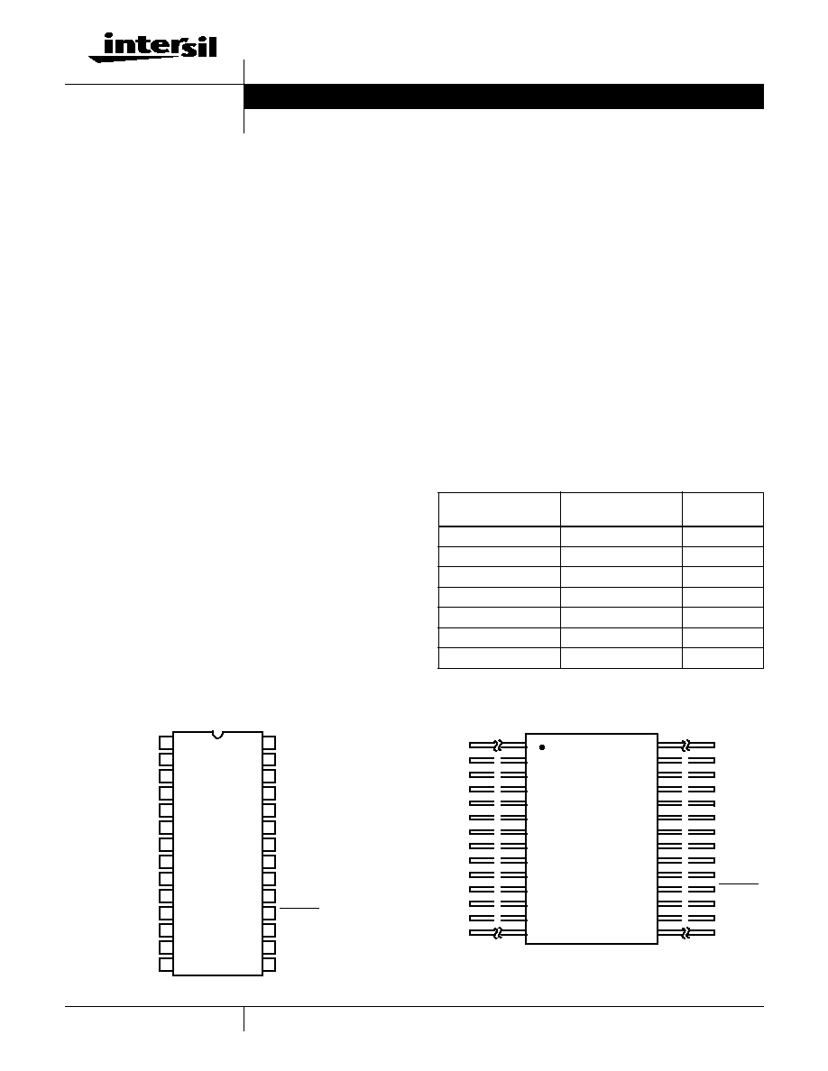
Pinouts
Ordering Information
ORDERING NUMBER
INTERNAL
MKT. NUMBER
TEMP. RANGE
(
o
C)
5962F9563002QXC
HS1-1840ARH-8
-55 to 125
5962F9563002QYC
HS9-1840ARH-8
-55 to 125
5962F9563002V9A
HS0-1840ARH-Q
25
5962F9563002VXC
HS1-1840ARH-Q
-55 to 125
5962F9563002VYC
HS9-1840ARH-Q
-55 to 125
HS1-1840ARH/PROTO HS1-1840ARH/PROTO
-55 to 125
HS9-1840ARH/PROTO HS9-1840ARH/PROTO
-55 to 125
HS1-1840ARH (SBDIP) CDIP2-T28
TOP VIEW
HS9-1840ARH (FLATPACK) CDFP3-F28
TOP VIEW
+V
S
NC
NC
IN 16
IN 15
IN 14
IN 13
IN 12
IN 11
IN 10
IN 9
GND
(+5V
S
) V
REF
ADDR A3
OUT
IN 8
IN 7
IN 6
IN 5
IN 3
IN 1
ENABLE
ADDR A0
ADDR A1
ADDR A2
-V
S
IN 4
IN 2
28
27
26
25
24
23
22
21
20
19
18
17
16
15
1
2
3
4
5
6
7
8
9
10
11
12
13
14
1
2
3
4
5
6
7
8
9
10
11
12
13
14
28
27
26
25
24
23
22
21
20
19
18
17
16
15
+V
S
NC
NC
IN 16
IN 15
IN 14
IN 13
IN 12
IN 11
IN 10
IN 9
GND
(+5V
S
) V
REF
ADDR A3
OUT
-V
S
IN 8
IN 7
IN 6
IN 5
IN 4
IN 3
IN 2
IN 1
ENABLE
ADDR A0
ADDR A1
ADDR A2
Data Sheet
August 1999
CAUTION: These devices are sensitive to electrostatic discharge; follow proper IC Handling Procedures.
1-888-INTERSIL or 321-724-7143 | Copyright © Intersil Corporation 1999

3
Burn-In/Life Test Circuits
NOTES:
V
S
+ = +15.5V
±
0.5V, V
S
- = -15.5V
±
0.5V.
R = 1k
±
5%.
C
1
= C
2
= 0.01
µ
F
±
10%, 1 each per socket, minimum.
D
1
= D
2
= 1N4002, 1 each per board, minimum.
Input Signals: square wave, 50% duty cycle, 0V to 15V peak
±
10%.
F1 = 100kHz; F2 = F1/2; F3 = F1/4; F4 = F1/8; F5 = F1/16.
FIGURE 1. DYNAMIC BURN-IN AND LIFE TEST CIRCUIT
NOTES:
R = 1k
±
5%,
1
/
4
W.
C
1
= C
2
= 0.01
µ
F minimum, 1 each per socket, minimum.
V
S
+ = 15.5V
±
0.5V, V
S
- = -15.5V
±
0.5V, V
R
= 15.5
±
0.5V.
FIGURE 2. STATIC BURN-IN TEST CIRCUIT
NOTES:
1. The above test circuits are utilized for all package types.
2. The Dynamic Test Circuit is utilized for all life testing.
Irradiation Circuit
HS-1840ARH
NOTE:
3. All irradiation testing is performed in the 28 lead CERDIP package.
R
R
GND
+V
S
R
28
27
26
25
24
23
22
21
20
19
18
17
16
15
1
2
3
4
5
6
7
8
9
10
11
12
13
14
F4
F3
F1
F5
F2
-V
S
10
11
12
13
14
28
27
26
25
24
23
22
21
20
19
18
17
16
15
1
2
3
4
5
6
7
8
9
R
R
R
GND
V
R
+V
S
R
-V
S
28
27
26
25
24
23
22
21
20
19
18
17
16
15
1k
+15V
+1V
+5V
NC
NC
-15V
1
2
3
4
5
6
7
8
9
10
11
12
13
14
HS-1840ARH
4
All Intersil semiconductor products are manufactured, assembled and tested under ISO9000 quality systems certification.
Intersil semiconductor products are sold by description only. Intersil Corporation reserves the right to make changes in circuit design and/or specifications at any time with-
out notice. Accordingly, the reader is cautioned to verify that data sheets are current before placing orders. Information furnished by Intersil is believed to be accurate and
reliable. However, no responsibility is assumed by Intersil or its subsidiaries for its use; nor for any infringements of patents or other rights of third parties which may result
from its use. No license is granted by implication or otherwise under any patent or patent rights of Intersil or its subsidiaries.
For information regarding Intersil Corporation and its products, see web site www.intersil.com
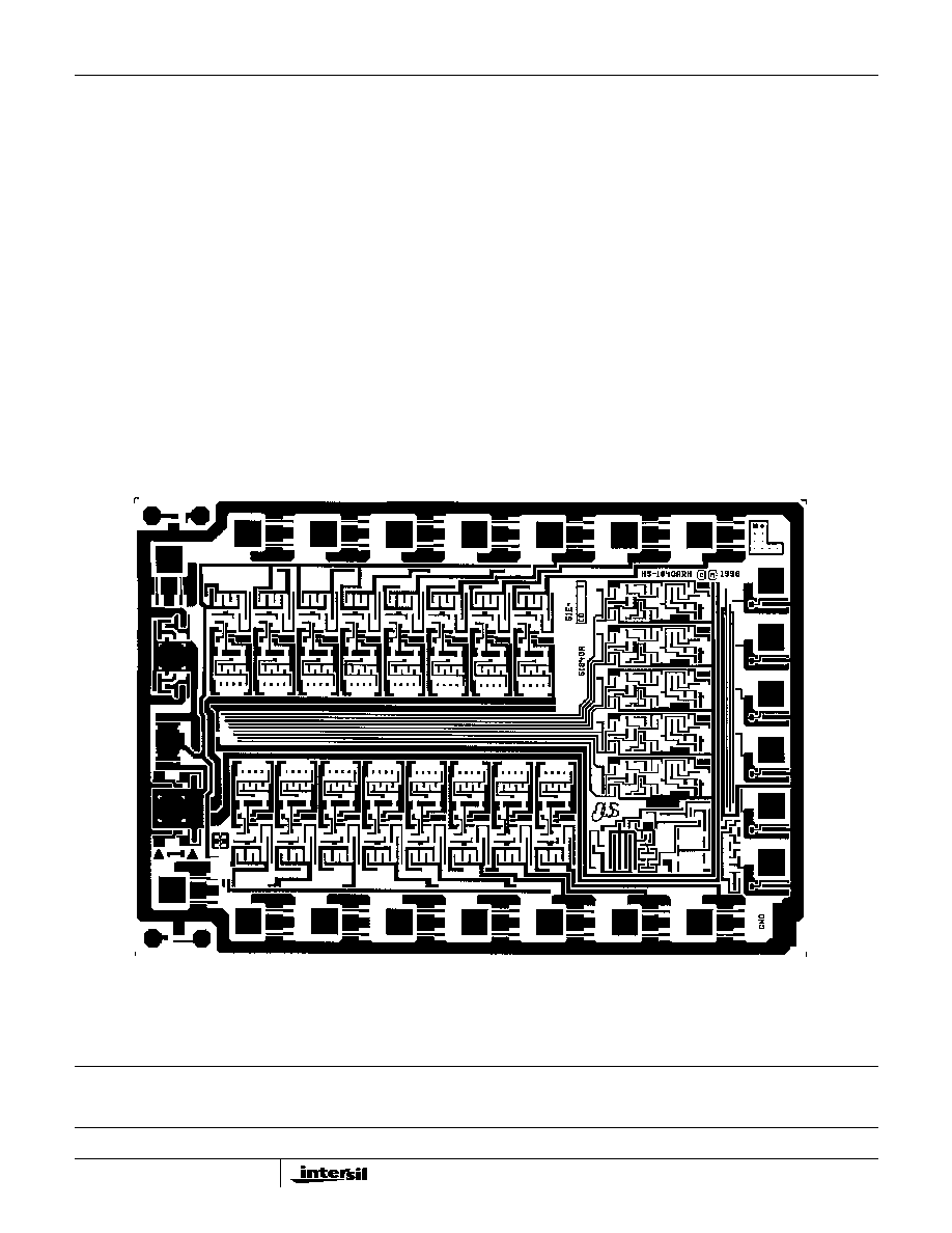
Die Characteristics
DIE DIMENSIONS:
(2820
µ
m x 4080
µ
m x 483
µ
m
±
25.4
µ
m)
111 mils x 161 mils x 19 mils
±
1 mil
INTERFACE MATERIALS:
Glassivation:
Type: PSG (Phosphorus Silicon Glass)
Thickness: 8.0k
≈
±
1k
≈
Top Metallization:
Type: AlSiCu
Thickness: 16.0k
≈
±
2k
≈
Backside Finish:
Silicon
ASSEMBLY RELATED INFORMATION:
Substrate Potential:
Unbiased (DI)
ADDITIONAL INFORMATION:
Worst Case Current Density:
Modified SEM
Transistor Count:
407
Process:
Radiation Hardened Silicon Gate,
Bonded Wafer, Dielectric Isolation
Metallization Mask Layout
HS-1840ARH
IN7
IN6
IN5
IN4
IN3
IN2
IN1
ENABLE
A0
A1
A2
A3
V
REF
GND
IN8
-V
OUT
+V
IN16
IN15
IN14
IN13
IN12
IN11
IN10
IN9
HS-1840ARH
