1
File Number
2485.7
HSP45116
Numerically Controlled
Oscillator/Modulator
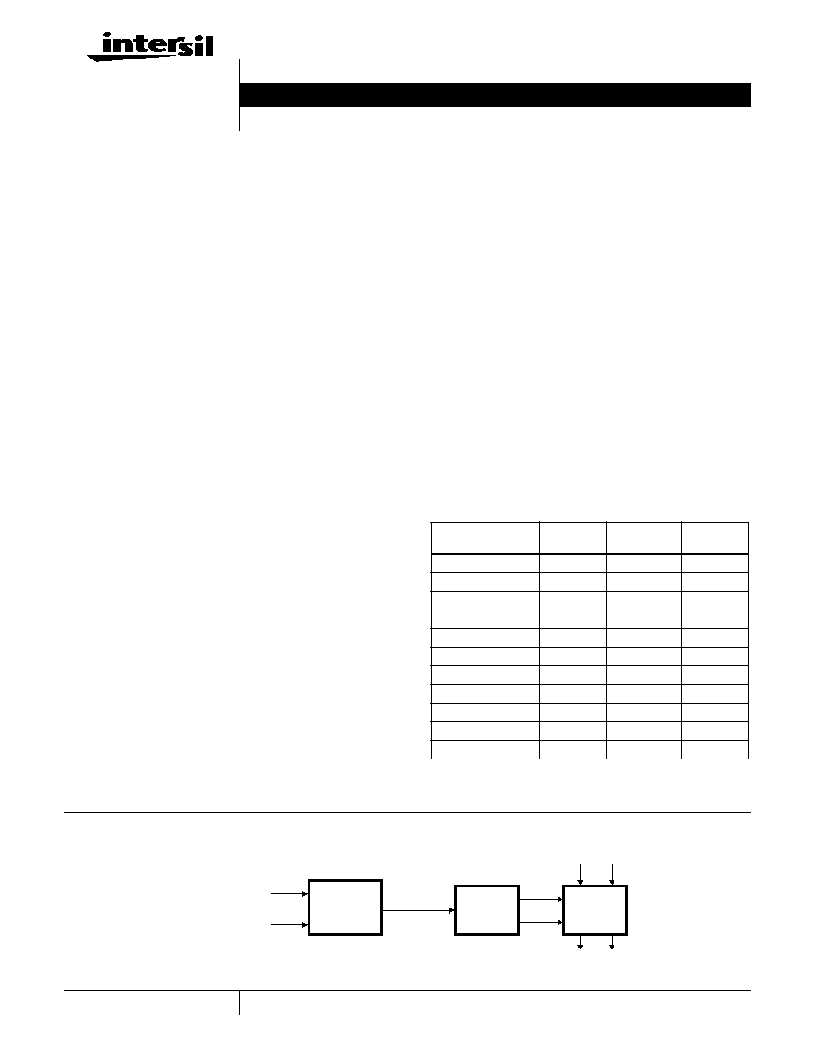
The Intersil HSP45116 combines a high performance
quadrature Numerically Controlled Oscillator (NCO) and a
high speed 16-bit Complex Multiplier/Accumulator (CMAC)
on a single IC. This combination of functions allows a
complex vector to be multiplied by the internally generated
(cos, sin) vector for quadrature modulation and
demodulation. As shown in the Block Diagram, the
HSP45116 is divided into three main sections. The
Phase/Frequency Control Section (PFCS) and the
Sine/Cosine Section together form a complex NCO. The
CMAC multiplies the output of the Sine/ Cosine Section with
an external complex vector.
The inputs to the Phase/Frequency Control Section consist
of a microprocessor interface and individual control lines.
The phase resolution of the PFCS is 32 bits, which results in
frequency resolution better than 0.008Hz at 33MHz. The
output of the PFCS is the argument of the sine and cosine.
The spurious free dynamic range of the complex sinusoid is
greater than 90dBc.
The output vector from the Sine/Cosine Section is one of the
inputs to the Complex Multiplier/Accumulator. The CMAC
multiplies this (cos, sin) vector by an external complex vector
and can accumulate the result. The resulting complex vectors
are available through two 20-bit output ports which maintain
the 90dB spectral purity. This result can be accumulated
internally to implement an accumulate and dump filter.
A quadrature down converter can be implemented by
loading a center frequency into the Phase/Frequency
Control Section. The signal to be down converted is the
Vector Input of the CMAC, which multiplies the data by the
rotating vector from the Sine/Cosine Section. The resulting
complex output is the down converted signal.
Features
∑ NCO and CMAC on One Chip
∑ 15MHz, 25.6MHz, 33MHz Versions
∑ 32-Bit Frequency Control
∑ 16-Bit Phase Modulation
∑ 16-Bit CMAC
∑ 0.008Hz Tuning Resolution at 33MHz
∑ Spurious Frequency Components < -90dBc
∑ Fully Static CMOS
Applications
∑ Frequency Synthesis
∑ Modulation - AM, FM, PSK, FSK, QAM
∑ Demodulation, PLL
∑ Phase Shifter
∑ Polar to Cartesian Conversions
Block Diagram
Ordering Information
PART NUMBER
TEMP.
RANGE (
o
C)
PACKAGE
PKG. NO.
HSP45116VC-15
0 to 70
160 Ld MQFP Q160.28x28
HSP45116VC-25
0 to 70
160 Ld MQFP Q160.28x28
HSP45116GC-15
0 to 70
145 Ld CPGA G145.A
HSP45116GC-25
0 to 70
145 Ld CPGA G145.A
HSP45116GC-33
0 to 70
145 Ld CPGA G145.A
HSP45116GI-15
-40 to 85
145 Ld CPGA G145.A
HSP45116GI-25
-40 to 85
145 Ld CPGA G145.A
HSP45116GI-33
-40 to 85
145 Ld CPGA G145.A
HSP45116GM-15/883
-55 to 125
145 Ld CPGA G145.A
HSP45116GM-25/883
-55 to 125
145 Ld CPGA G145.A
HSP45116AVC-52
0 to 70
160 Ld MQFP Q160.28x28
This part has its own data sheet under HSP45116A, AnswerFAX
document no. 4156.
PHASE/
FREQUENCY
CONTROL
SECTION
SINE/
COSINE
SECTION
CMAC
SINE/
COSINE
ARGUMENT
SIN
COS
VECTOR INPUT
VECTOR OUTPUT
R
I
R
I
MICROPROCESSOR
INTERFACE
INDIVIDUAL
CONTROL SIGNALS
Data Sheet
May 1999
CAUTION: These devices are sensitive to electrostatic discharge; follow proper IC Handling Procedures.
http://www.intersil.com or 407-727-9207
|
Copyright
©
Intersil Corporation 1999
5
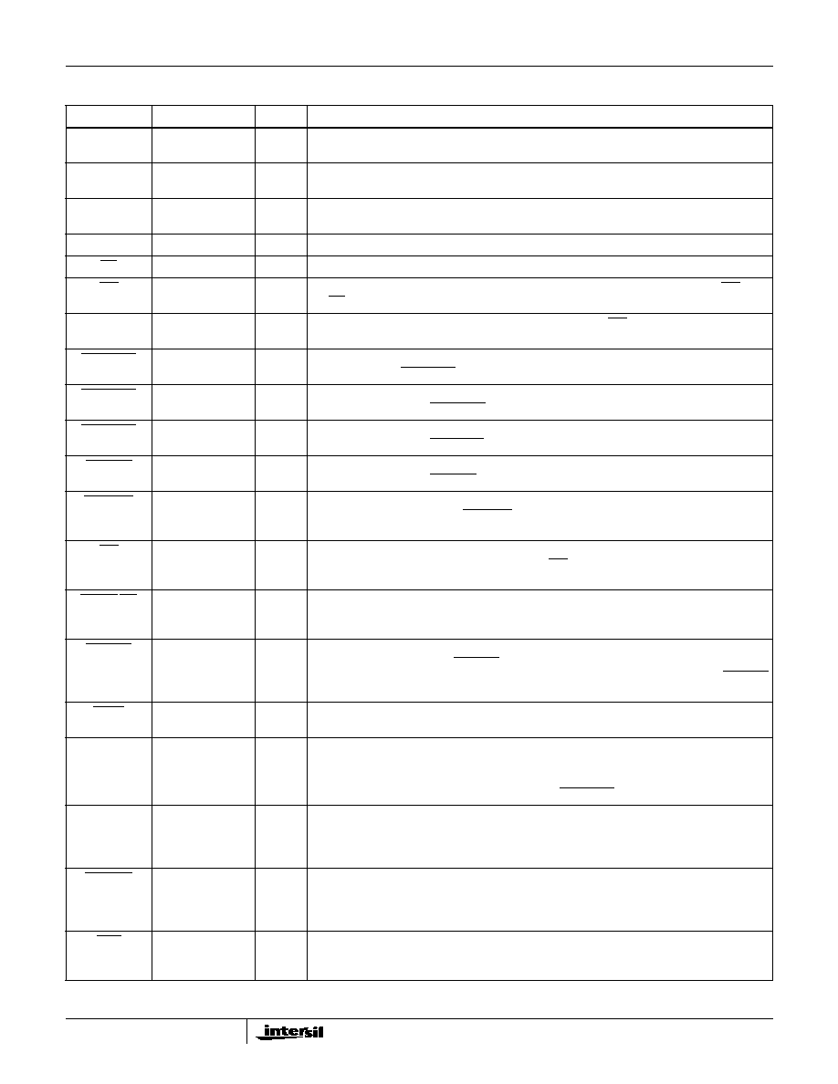
Pin Description
NAME
NUMBER
TYPE
DESCRIPTION
V
CC
A1, A9, A15, G1,
J15, Q1, Q7, Q15
-
+5V Power supply input.
GND
A8, A14, B1, H1,
H15, P15, Q2, Q8
-
Power supply ground input.
C0-15
N8-11, P8-13,
Q9-14
I
Control input bus for loading phase and frequency data into the PFCS. C15 is the MSB.
AD0-1
N7, P7
I
Address pins for selecting destination of C0-15 data.
CS
P6
I
Chip Select (active low).
WR
Q6
I
Write Enable. Data is clocked into the register selected by AD0-1 on the rising edge of WR when
the CS line is low.
CLK
Q5
I
Clock. All registers, except the control registers clocked with WR, are clocked (when enabled)
by the rising edge of CLK.
ENPHREG
M1
I
Phase Register Enable (active low). Registered on chip by CLK. When active, after being
clocked onto chip, ENPHREG enables the clocking of data into the phase register.
ENOFREG
N1
I
Frequency Offset Register Enable (active Low). Registered on chip by CLK. When active, after
being clocked onto chip, ENOFREG enables clocking of data into the frequency offset register.
ENCFREG
N5
I
Center Frequency Register Enable (active low). Registered on chip by CLK. When active, after
being clocked onto chip, ENCFREG enables clocking of data into the center frequency register.
ENPHAC
Q3
I
Phase Accumulator Register Enable (active low). Registered on chip by CLK. When active, after
being clocked onto chip, ENPHAC enables clocking of the phase accumulator register.
ENTIREG
P5
I
Time Interval Control Register Enable (active low). Registered on chip by CLK. When active,
after being clocked onto chip, ENTIREG enables clocking of data into the time accumulator
register.
ENI
Q4
I
Real and Imaginary Data Input Register (RIR, IIR) Enable (active low). Registered on chip by
CLK. When active, after being clocked onto chip, ENI enables clocking of data into the real and
imaginary input data register.
MODPI/2PI
N6
I
Modulo
/2
Select. When low, the Sine and Cosine ROMs are addressed modulo 2
(360
degrees). When high, the most significant address bit is held low so that the ROMs are
addressed modulo
(180 degrees). This input is registered on chip by clock.
CLROFR
P4
I
Frequency Offset Register Output Zero (active low). Registered on chip by CLK. When active,
after being clocked onto chip, CLROFR zeros the data path from the frequency offset register to
the frequency adder. New data can still be clocked into the frequency offset register; CLROFR
does not affect the contents of the register.
LOAD
N4
I
Phase Accumulator Load Control (active low). Registered on chip by CLK. Zeroes feedback path
in the phase accumulator without clearing the phase accumulator register.
MOD0-1
M3, N3
I
External Modulation Control Bits. When selected with the PMSEL line, these bits add a 0, 90,
180, or 270 degree offset to the current phase in the phase accumulator. The lower 14 bits of
the phase control path are set to zero.
These bits are loaded into the phase register when ENPHREG is low.
PMSEL
P3
I
Phase Modulation Select Line. This line determines the source of the data clocked into the phase
register. When high, the phase control register is selected. When low, the external modulation pins
(MOD0-1) are selected for the most significant two bits and the least significant two bits and the
least significant 14 bits are set to zero. This control is registered by CLK.
RBYTILD
L3
I
ROM Bypass, Timer Load. Active low, registered by CLK. This input bypasses the sine/ cosine
ROM so that the 16-bit phase adder output and lower 16 bits of the phase accumulator go
directly to the CMAC's sine and cosine inputs, respectively. It also enables loading of the timer
accumulator register by zeroing the feedback in the accumulator.
PACI
P2
I
Phase Accumulator Carry Input (active low). A low on this pin causes the phase accumulator to
increment by one, in addition to the values in the phase accumulator register and frequency
adder.
HSP45116