 | –≠–ª–µ–∫—Ç—Ä–æ–Ω–Ω—ã–π –∫–æ–º–ø–æ–Ω–µ–Ω—Ç: ICL3207 | –°–∫–∞—á–∞—Ç—å:  PDF PDF  ZIP ZIP |
1
Æ
FN4892.5
ICL3207, ICL3217
Low Power, +3V to +5.5V, 250kbps,
RS-232 Transmitters/Receivers
The Intersil ICL32X7 devices are 3.0V to 5.5V powered
RS-232 transmitters (five)/receivers (three) which meet
ElA/TIA-232 and V.28/V.24 specifications, even at
V
CC
= 3.0V. Targeted applications are ISDN Terminal
Adaptors, PDAs, Palmtops, peripherals, and notebook and
laptop computers where the low operational, and even lower
standby, power consumption is critical. The ICL3217's
efficient on-chip charge pumps, coupled with an automatic
powerdown function, reduces the standby supply current to
a 1
µ
A trickle. Small footprint packaging, and the use of
small, low value capacitors ensure board space savings as
well. Data rates greater than 250kbps are guaranteed at
worst case load conditions. This family is fully compatible
with 3.3V only systems, mixed 3.3V and 5.0V systems, and
5.0V only systems, and is a lower power, pin-for-pin
replacement for `207 and `237 type devices.
The ICL3217 features an automatic powerdown function
which powers down the on-chip power-supply and driver
circuits. This occurs when an attached peripheral device is
shut off or the RS-232 cable is removed, conserving system
power automatically, without changes to the hardware or
operating system. The ICL3217 powers up again when a
valid RS-232 voltage is applied to any receiver input.
Table 1 summarizes the features of the devices represented
by this data sheet, while application Note AN9863
summarizes the features of each device comprising the
ICL32XX 3V family.
Features
∑ Pb-free Available as an Option (see Ordering Info)
∑
±
15kV ESD Protected (Human Body Model)
∑ 5V Lower Power Replacement for MAX207, HIN207,
HIN237
∑ Meets EIA/TIA-232 and V.28/V.24 Specifications at 3V
∑ Latch-Up Free
∑ On-Chip Voltage Converters Require Only Four External
0.1
µ
F Capacitors
∑ Automatic Powerdown (I
CC
= 1
µ
A, ICL3217 Only)
∑ Receiver Hysteresis For Improved Noise Immunity
∑ Guaranteed Minimum Data Rate . . . . . . . . . . . . . 250kbps
∑ Guaranteed Minimum Slew Rate . . . . . . . . . . . . . . . 6V/
µ
s
∑ Wide Power Supply Range . . . . . . . Single +3V to +5.5V
Applications
∑ Any System Requiring RS-232 Communication Ports
- Battery Powered, Hand-Held, and Portable Equipment
- Laptop Computers, Notebooks, Palmtops
- Modems, Printers and other Peripherals
- ISDN Terminal Adaptors and Set Top Boxes
Related Literature
∑ Technical Brief TB363 "Guidelines for Handling and
Processing Moisture Sensitive Surface Mount Devices
(SMDs)"
TABLE 1. SUMMARY OF FEATURES
PART NUMBER
NO. OF
Tx.
NO. OF
Rx.
NO. OF MONITOR
Rx. (R
OUTB
)
DATA RATE
(kbps)
Rx. ENABLE
FUNCTION?
MANUAL
POWER-
DOWN?
AUTOMATIC
POWERDOWN
FUNCTION?
ICL3207
5
3
0
250
NO
NO
NO
ICL3217
5
3
0
250
NO
NO
YES
Data Sheet
July 2004
CAUTION: These devices are sensitive to electrostatic discharge; follow proper IC Handling Procedures.
1-888-INTERSIL or 321-724-7143
|
Intersil (and design) is a registered trademark of Intersil Americas Inc.
Copyright © Intersil Americas Inc. 2001, 2004. All Rights Reserved
2
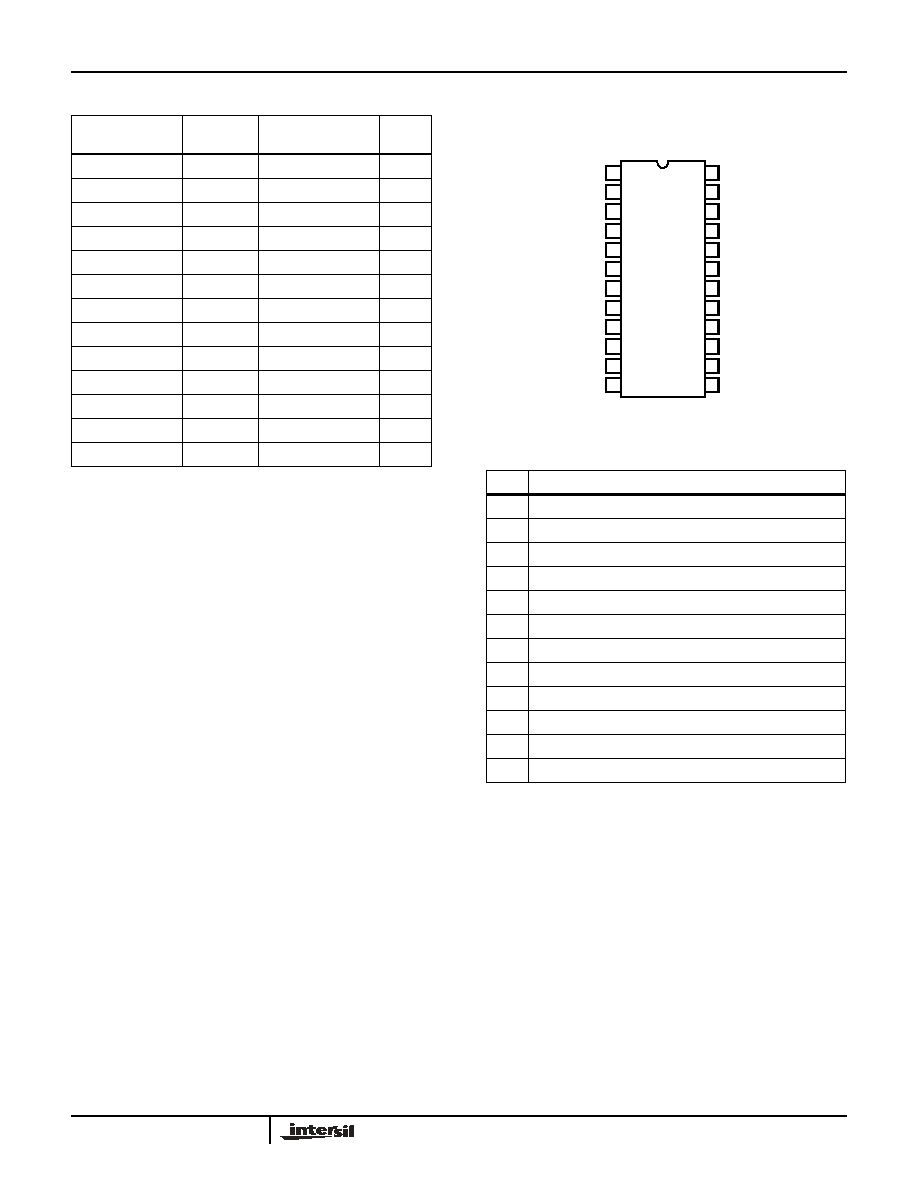
Pinout
ICL3207, ICL3217 (SOIC, SSOP)
TOP VIEW
Ordering Information
PART NO.*
TEMP.
RANGE (∞C)
PACKAGE
PKG.
DWG. #
ICL3207CA
0 to 70
24 Ld SSOP
M24.209
ICL3207CAZ (Note)
0 to 70
24 Ld SSOP
(Pb-free)
M24.209
ICL3207CB
0 to 70
24 Ld SOIC
M24.3
ICL3207CBZ (Note)
0 to 70
24 Ld SOIC
(Pb-free)
M24.3
ICL3207IA
-40 to 85
24 Ld SSOP
M24.209
ICL3207IAZ (Note)
-40 to 85
24 Ld SSOP
(Pb-free)
M24.209
ICL3217CA
0 to 70
24 Ld SSOP
M24.209
ICL3217CAZ (Note)
0 to 70
24 Ld SSOP
(Pb-free)
M24.209
ICL3217CB
0 to 70
24 Ld SOIC
M24.3
ICL3217CBZ (Note)
0 to 70
24 Ld SOIC
(Pb-free)
M24.3
ICL3217IA
-40 to 85
24 Ld SSOP
M24.209
ICL3217IAZ (Note)
-40 to 85
24 Ld SSOP
(Pb-free)
M24.209
ICL3217IB
-40 to 85
24 Ld SOIC
M24.3
*Most surface mount devices are available on tape and reel; add
"-T" to suffix.
NOTE: Intersil Pb-free products employ special Pb-free material
sets; molding compounds/die attach materials and 100% matte tin
plate termination finish, which is compatible with both SnPb and
Pb-free soldering operations. Intersil Pb-free products are MSL
classified at Pb-free peak reflow temperatures that meet or exceed
the Pb-free requirements of IPC/JEDEC J Std-020B.
Pin Descriptions
PIN
FUNCTION
V
CC
System power supply input (3.0V to 5.5V).
V+
Internally generated positive transmitter supply (+5.5V).
V-
Internally generated negative transmitter supply (-5.5V).
GND Ground connection.
C1+
External capacitor (voltage doubler) is connected to this lead.
C1-
External capacitor (voltage doubler) is connected to this lead.
C2+
External capacitor (voltage inverter) is connected to this lead.
C2-
External capacitor (voltage inverter) is connected to this lead.
T
IN
TTL/CMOS compatible transmitter Inputs.
T
OUT
RS-232 level (nominally
±
5.5V) transmitter Outputs.
R
IN
RS-232 compatible receiver inputs.
R
OUT
TTL/CMOS level receiver outputs.
T3
OUT
T1
OUT
T2
OUT
R1
IN
R1
OUT
T2
IN
T1
IN
GND
V
CC
C1+
V+
C1-
T4
OUT
R2
OUT
T5
IN
T5
OUT
T4
IN
R3
OUT
V-
C2-
C2+
R2
IN
T3
IN
R3
IN
1
2
3
4
5
6
7
8
9
10
11
12
16
17
18
19
20
21
22
23
24
15
14
13
ICL3207, ICL3217
3
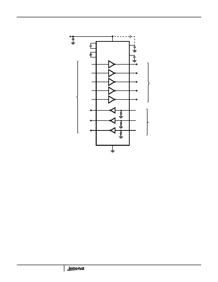
Typical Operating Circuit
ICL32X7
9
V
CC
T1
OUT
T2
OUT
T3
OUT
T1
IN
T2
IN
T3
IN
T
1
T
2
T
3
+
+
7
6
2
3
18
1
10
12
11
15
V+
V-
C1+
C1-
C2+
C2-
+
13
14
R1
OUT
R1
IN
4
5k
R2
OUT
R2
IN
23
22
5k
R3
OUT
R3
IN
16
17
5k
5
C
1
C
2
+
C
3
C
4
GND
V
CC
+
0.1
µ
F
8
TTL/CMOS
LOGIC LEVELS
RS-232
LEVELS
RS-232
LEVELS
R
1
R
2
R
3
T4
OUT
T5
OUT
T4
IN
T5
IN
T
5
19
24
21
20
T
4
- FOR V
CC
= 3.3V, C
1
- C
4
= 0.1
µ
F or 0.22
µ
F
FOR V
CC
= 5V, C
1
- C
4
= 0.1
µ
F OR 1
µ
F
+
C
3
(OPTIONAL CONNECTION)
ICL3207, ICL3217
4
Absolute Maximum Ratings
Thermal Information
V
CC
to Ground. . . . . . . . . . . . . . . . . . . . . . . . . . . . . . . . -0.3V to 6V
V+ to Ground . . . . . . . . . . . . . . . . . . . . . . . . . . . . . . . . . -0.3V to 7V
V- to Ground . . . . . . . . . . . . . . . . . . . . . . . . . . . . . . . . +0.3V to -7V
V+ to V- . . . . . . . . . . . . . . . . . . . . . . . . . . . . . . . . . . . . . . . . . . . 14V
Input Voltages
T
IN
. . . . . . . . . . . . . . . . . . . . . . . . . . . . . . . . . . . . . . . -0.3V to 6V
R
IN
. . . . . . . . . . . . . . . . . . . . . . . . . . . . . . . . . . . . . . . . . . . .
±
25V
Output Voltages
T
OUT
. . . . . . . . . . . . . . . . . . . . . . . . . . . . . . . . . . . . . . . . .
±
13.2V
R
OUT
. . . . . . . . . . . . . . . . . . . . . . . . . . . . . . -0.3V to V
CC
+ 0.3V
Short Circuit Duration
T
OUT
. . . . . . . . . . . . . . . . . . . . . . . . . . . . . . . . . . . . . Continuous
ESD Rating . . . . . . . . . . . . . . . . . . . . . . . . See Specification Table
Thermal Resistance (Typical, Note 1)
JA
(∞C/W)
24 Ld SOIC Package . . . . . . . . . . . . . . . . . . . . . . . .
74
24 Ld SSOP Package . . . . . . . . . . . . . . . . . . . . . . .
100
Maximum Junction Temperature (Plastic Package) . . . . . . . 150∞C
Maximum Storage Temperature Range . . . . . . . . . . -65∞C to 150∞C
Maximum Lead Temperature (Soldering 10s) . . . . . . . . . . . . 300∞C
(Lead Tips Only)
Operating Conditions
Temperature Range
ICL32X7CX . . . . . . . . . . . . . . . . . . . . . . . . . . . . . . . . . . 0∞C to 70∞C
ICL32X7IX . . . . . . . . . . . . . . . . . . . . . . . . . . . . . . . . . . -40∞C to 85∞C
CAUTION: Stresses above those listed in "Absolute Maximum Ratings" may cause permanent damage to the device. This is a stress only rating and operation of the
device at these or any other conditions above those indicated in the operational sections of this specification is not implied.
NOTE:
1.
JA
is measured with the component mounted on a low effective thermal conductivity test board in free air. See Tech Brief TB379 for details.
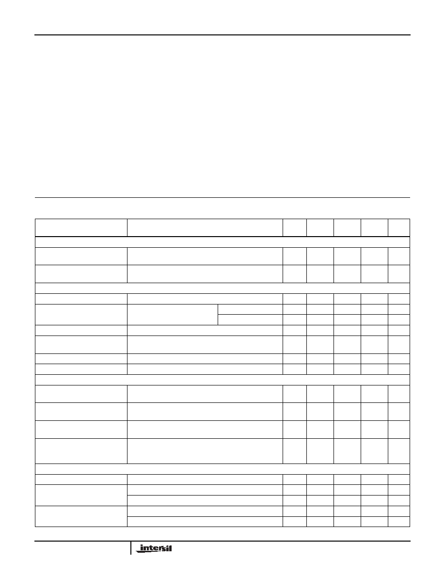
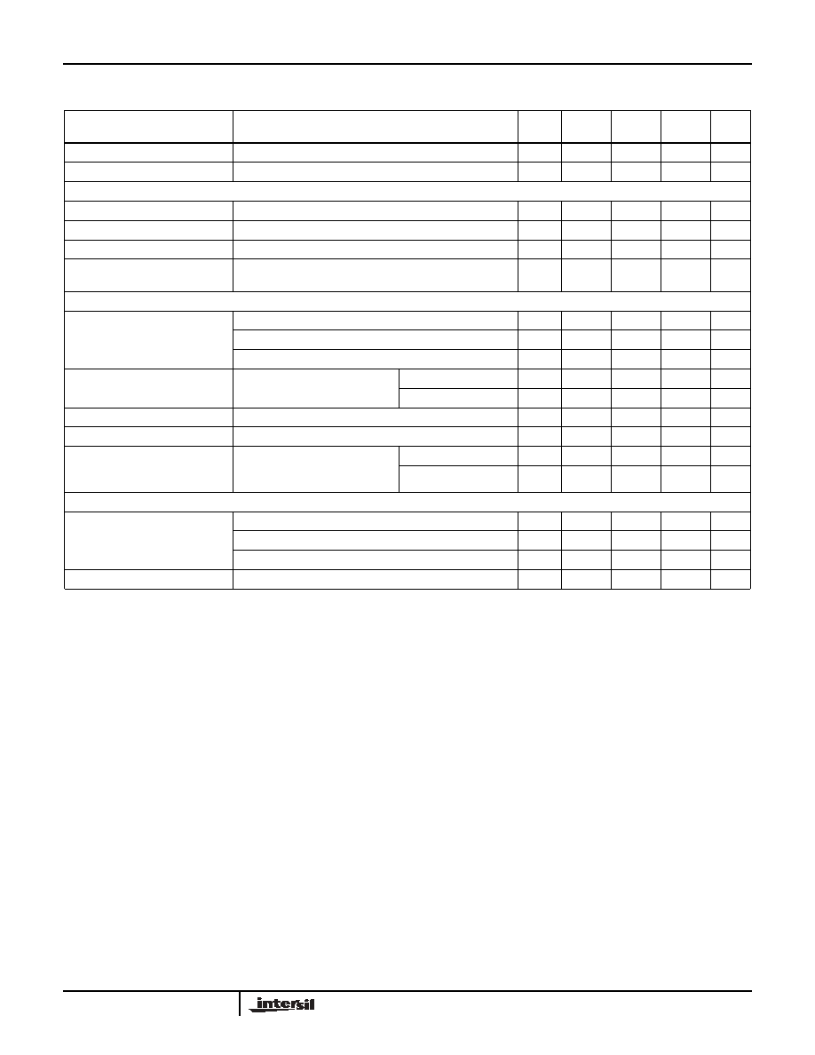
Electrical Specifications
Test Conditions: V
CC
= 3V to 5.5V, C
1
- C
4
= 0.1
µ
F; Unless Otherwise Specified.
Typicals are at T
A
= 25∞C
PARAMETER
TEST CONDITIONS
TEMP
(∞C)
MIN
TYP
MAX
UNITS
DC CHARACTERISTICS
Supply Current, Automatic
Powerdown
All R
IN
Open (ICL3217 Only)
25
-
1.0
10
µ
A
Supply Current,
Automatic Powerdown Disabled
All Outputs Unloaded
25
-
0.3
1.0
mA
TRANSMITTER INPUTS AND RECEIVER OUTPUTS
Input Logic Threshold Low
T
IN
Full
-
-
0.8
V
Input Logic Threshold High
T
IN
V
CC
= 3.3V
Full
2.0
-
-
V
V
CC
= 5.0V
Full
2.4
-
-
V
Input Leakage Current
T
IN
Full
-
±
0.01
±
1.0
µ
A
Output Leakage Current
(ICL3217 Only)
Full
-
±
0.05
±
10
µ
A
Output Voltage Low
I
OUT
= 1.6mA
Full
-
-
0.4
V
Output Voltage High
I
OUT
= -1.0mA
Full
V
CC
-0.6 V
CC
-0.1
-
V
AUTOMATIC POWERDOWN (ICL3217 Only)
Receiver Input Thresholds to
Enable Transmitters
ICL3217 Powers Up (Figure 4)
Full
-2.7
-
2.7
V
Receiver Input Thresholds to
Disable Transmitters
ICL3217 Powers Down (Figure 4)
Full
-0.3
-
0.3
V
Receiver Threshold to Transmitters
Enabled Delay (t
WU
)
25
-
100
-
µ
s
Receiver Positive or Negative
Threshold to Transmitters
Disabled Delay
25
-
30
-
µ
s
RECEIVER INPUTS
Input Voltage Range
Full
-25
-
25
V
Input Threshold Low
V
CC
= 3.3V
25
0.6
1.2
-
V
V
CC
= 5.0V
25
0.8
1.5
-
V
Input Threshold High
V
CC
= 3.3V
25
-
1.5
2.4
V
V
CC
= 5.0V
25
-
1.8
2.4
V
ICL3207, ICL3217
5
Detailed Description
The ICL32X7 interface ICs operate from a single +3V to
+5.5V power supply, guarantee a 250kbps minimum data
rate, require only four small external 0.1
µ
F capacitors,
feature low power consumption, and meet all ElA RS-232C
and V.28 specifications. The circuit is divided into three
sections: The charge pump, the transmitters, and the
receivers.
Charge-Pump
Intersil's new ICL32XX family utilizes regulated on-chip dual
charge pumps as voltage doublers, and voltage inverters to
generate
±
5.5V transmitter supplies from a V
CC
supply as
low as 3.0V. This allows these devices to maintain RS-232
compliant output levels over the
±
10% tolerance range of
3.3V powered systems. The efficient on-chip power supplies
require only four small, external 0.1
µ
F capacitors for the
voltage doubler and inverter functions at V
CC
= 3.3V. See
the "Capacitor Selection" section, and Table 3 for capacitor
recommendations for other operating conditions. The charge
pumps operate discontinuously (i.e., they turn off as soon as
the V+ and V- supplies are pumped up to the nominal values),
resulting in significant power savings.
Transmitters
The transmitters are proprietary, low dropout, inverting
drivers that translate TTL/CMOS inputs to EIA/TIA-232
output levels. Coupled with the on-chip
±
5.5V supplies,
these transmitters deliver true RS-232 levels over a wide
range of single supply system voltages.
ICL3217 transmitter outputs disable and assume a high
impedance state when the device enters the automatic
powerdown mode. These outputs may be driven to
±
12V
when disabled.
Both devices guarantee a 250kbps data rate for full load
conditions (3k
and 1000pF), V
CC
3.0V, with one
transmitter operating at full speed. Under more typical
conditions of V
CC
3.3V, R
L
= 3k
, and C
L
= 250pF, one
transmitter easily operates at 800kbps.
Transmitter inputs float if left unconnected, and may cause
I
CC
increases. Connect unused inputs to GND for the best
performance.
Input Hysteresis
25
-
0.3
-
V
Input Resistance
25
3
5
7
k
TRANSMITTER OUTPUTS
Output Voltage Swing
All Transmitter Outputs Loaded with 3k
to Ground
Full
±
5.0
±
5.4
-
V
Output Resistance
V
CC
= V+ = V- = 0V, Transmitter Output =
±
2V
Full
300
10M
-
Output Short-Circuit Current
Full
-
±
35
±
60
mA
Output Leakage Current
(ICL3217 Only)
V
OUT
=
±
12V, V
CC
= 0V or 3V to 5.5V
In Automatic Powerdown
Full
-
-
±
25
µ
A
TIMING CHARACTERISTICS
Maximum Data Rate
(One Transmitter Switching)
V
CC
= 3.15V, C
1
- C
4
= 0.1
µ
F, R
L
= 3k
,
C
L
= 1000pF
Full
250
500
-
kbps
V
CC
= 3.0V, C
1
- C
4
= 0.22
µ
F, R
L
= 3k
,
C
L
= 1000pF
Full
250
286
-
kbps
V
CC
4.5V, C
1
- C
4
= 0.1
µ
F, R
L
= 3k
,
C
L
= 1000pF
Full
250
310
-
kbps
Receiver Propagation Delay
Receiver Input to Receiver
Output, C
L
= 150pF
t
PHL
25
-
0.3
-
µ
s
t
PLH
25
-
0.3
-
µ
s
Transmitter Skew
t
PHL
- t
PLH
Full
-
200
1000
ns
Receiver Skew
t
PHL
- t
PLH
Full
-
100
500
ns
Transition Region Slew Rate
V
CC
= 3.3V, R
L
= 3k
to 7k
,
Measured From +3V to -3V or -3V
to +3V
C
L
= 200pF to 2500pF
25
4
15
30
V/
µ
s
C
L
= 200pF to 1000pF
25
6
15
30
V/
µ
s
ESD PERFORMANCE
RS-232 Pins (T
OUT
, R
IN
)
Human Body Model
25
-
±
15
-
kV
IEC1000-4-2 Contact Discharge
25
-
±
8
-
kV
IEC1000-4-2 Air Gap Discharge
25
-
±
6
-
kV
All Other Pins
Human Body Model
25
-
±
2
-
kV
Electrical Specifications
Test Conditions: V
CC
= 3V to 5.5V, C
1
- C
4
= 0.1
µ
F; Unless Otherwise Specified.
Typicals are at T
A
= 25∞C (Continued)
PARAMETER
TEST CONDITIONS
TEMP
(∞C)
MIN
TYP
MAX
UNITS
ICL3207, ICL3217