1
TM
File Number 4914.4
CAUTION: These devices are sensitive to electrostatic discharge; follow proper IC Handling Procedures.
1-888-INTERSIL or 321-724-7143
|
Intersil (and design) is a trademark of Intersil Americas Inc.
Copyright © Intersil Americas Inc. 2001. All Rights Reserved
ICL3207E, ICL3217E
+/- 15kV ESD Protected, +3V to +5.5V, Low
Power, 250kbps, RS-232
Transmitters/Receivers
The Intersil ICL32X7E devices are 3V to 5.5V powered
RS-232 transmitters (five)/receivers (three) which meet
ElA/TIA-232 and V.28/V.24 specifications, even at
V
CC
= 3.0V. Additionally, they provide
±
15kV ESD protection
(IEC 1000-4-2 Air Gap) and
±
15kV Human Body Model
protection on transmitter outputs and receiver inputs
(RS-232 pins). Targeted applications are ISDN Terminal
Adaptors, PDAs, Palmtops, peripherals, and notebook and
laptop computers where the low operational, and even lower
standby, power consumption is critical. The ICL3217E's
efficient on-chip charge pumps, coupled with an automatic
powerdown function, reduces the standby supply current to
a 1
µA trickle. Small footprint packaging, and the use of
small, low value capacitors ensure board space savings as
well. Data rates greater than 250kbps are guaranteed at
worst case load conditions. This family is fully compatible
with 3.3V-only systems, mixed 3.3V and 5V systems, and
5V-only systems, and is a lower power, pin-for-pin
replacement for `207E and `237E type devices.
The ICL3217E features an automatic powerdown function
which powers down the on-chip power-supply and driver
circuits. This occurs when an attached peripheral device is
shut off or the RS-232 cable is removed, conserving system
power automatically, without changes to the hardware or
operating system. The ICL3217E powers up again when a
valid RS-232 voltage is applied to any receiver input.
Table 1 summarizes the features of the devices represented
by this data sheet, while application Note AN9863
summarizes the features of each device comprising the
ICL32XXE 3V family.
Features
∑ ESD Protection for RS-232 I/O Pins to
±
15kV (IEC1000)
∑ 5V Lower Power Replacement for MAX207E, HIN207E,
HIN237E
∑ Meets EIA/TIA-232 and V.28/V.24 Specifications at 3V
∑ Latch-Up Free
∑ On-Chip Voltage Converters Require Only Four External
0.1
µF Capacitors
∑ Automatic Powerdown (I
CC
= 1
µA, ICL3217E Only)
∑ Receiver Hysteresis For Improved Noise Immunity
∑ Guaranteed Minimum Data Rate . . . . . . . . . . . . . 250kbps
∑ Guaranteed Minimum Slew Rate . . . . . . . . . . . . . . . 6V/
µs
∑ Wide Power Supply Range . . . . . . . Single +3V to +5.5V
Applications
∑ Any System Requiring RS-232 Communication Ports
- Battery Powered, Hand-Held, and Portable Equipment
- Laptop Computers, Notebooks, Palmtops
- Modems, Printers and other Peripherals
- ISDN Terminal Adaptors and Set Top Boxes
∑ Related Literature
- Technical Brief TB363, Guidelines for Handling and
Processing Moisture Sensitive Surface Mount
Devices (SMDs)
- Application Note AN9863, 3V to +5.5V, 250k-1Mbps,
RS-232 Transmitters/Receivers
Ordering Information
(NOTE 1)
PART NO.
TEMP.
RANGE (
o
C)
PACKAGE
PKG. NO.
ICL3207ECA
0 to 70
24 Ld SSOP
M24.209
ICL3207EIA
-40 to 85
24 Ld SSOP
M24.209
ICL3207ECB
0 to 70
24 Ld SOIC
M24.3
ICL3207EIB
-40 to 85
24 Ld SOIC
M24.3
ICL3217ECA
0 to 70
24 Ld SSOP
M24.209
ICL3217EIA
-40 to 85
24 Ld SSOP
M24.209
ICL3217ECB
0 to 70
24 Ld SOIC
M24.3
ICL3217EIB
-40 to 85
24 Ld SOIC
M24.3
NOTE:
1. Most surface mount devices are available on tape and reel; add
"-T" to suffix.
TABLE 1. SUMMARY OF FEATURES
PART NUMBER
NO. OF
TX
NO. OF
RX
NO. OF MONITOR
RX (R
OUTB
)
DATA RATE
(kbps)
RX ENABLE
FUNCTION?
MANUAL
POWER-
DOWN?
AUTOMATIC
POWERDOWN
FUNCTION?
ICL3207E
5
3
0
250
NO
NO
NO
ICL3217E
5
3
0
250
NO
NO
YES
Data Sheet
November 2001

2
Pinout
ICL3207E, ICL3217E (SOIC, SSOP)
TOP VIEW
T3
OUT
T1
OUT
T2
OUT
R1
IN
R1
OUT
T2
IN
T1
IN
GND
V
CC
C1+
V+
C1-
T4
OUT
R2
OUT
T5
IN
T5
OUT
T4
IN
R3
OUT
V-
C2-
C2+
R2
IN
T3
IN
R3
IN
1
2
3
4
5
6
7
8
9
10
11
12
16
17
18
19
20
21
22
23
24
15
14
13
Pin Descriptions
PIN
FUNCTION
V
CC
System power supply input (3.0V to 5.5V).
V+
Internally generated positive transmitter supply (+5.5V).
V-
Internally generated negative transmitter supply (-5.5V).
GND Ground connection.
C1+ External capacitor (voltage doubler) is connected to this lead.
C1-
External capacitor (voltage doubler) is connected to this lead.
C2+ External capacitor (voltage inverter) is connected to this lead.
C2-
External capacitor (voltage inverter) is connected to this lead.
T
IN
TTL/CMOS compatible transmitter inputs.
T
OUT
±15kV ESD Protected
,
RS-232 level (nominally
±5.5V)
transmitter outputs.
R
IN
±15kV ESD Protected
,
RS-232 compatible receiver inputs.
R
OUT
TTL/CMOS level receiver outputs.
Typical Operating Circuit
ICL32X7E
9
V
CC
T1
OUT
T2
OUT
T3
OUT
T1
IN
T2
IN
T3
IN
T
1
T
2
T
3
+
+
7
6
2
3
18
1
10
12
11
15
V+
V-
C1+
C1-
C2+
C2-
+
13
14
R1
OUT
R1
IN
4
5k
R2
OUT
R2
IN
23
22
5k
R3
OUT
R3
IN
16
17
5k
5
C
1
C
2
+
C
3
C
4
GND
V
CC
+
0.1
µF
8
TTL/CMOS
LOGIC LEVELS
RS-232
LEVELS
RS-232
LEVELS
R
1
R
2
R
3
T4
OUT
T5
OUT
T4
IN
T5
IN
T
5
19
24
21
20
T
4
- FOR V
CC
= 3.3V, C
1
- C
4
= 0.1
µF or 0.22µF
FOR V
CC
= 5V, C
1
- C
4
= 0.1
µF OR 1µF
+
C
3
(OPTIONAL CONNECTION)
ICL3207E, ICL3217E
3
Absolute Maximum Ratings
Thermal Information
V
CC
to Ground. . . . . . . . . . . . . . . . . . . . . . . . . . . . . . . . -0.3V to 6V
V+ to Ground . . . . . . . . . . . . . . . . . . . . . . . . . . . . . . . . . -0.3V to 7V
V- to Ground. . . . . . . . . . . . . . . . . . . . . . . . . . . . . . . . . +0.3V to -7V
V+ to V- . . . . . . . . . . . . . . . . . . . . . . . . . . . . . . . . . . . . . . . . . . . 14V
Input Voltages
T
IN
. . . . . . . . . . . . . . . . . . . . . . . . . . . . . . . . . . . . . . . -0.3V to 6V
R
IN
. . . . . . . . . . . . . . . . . . . . . . . . . . . . . . . . . . . . . . . . . . . .
±25V
Output Voltages
T
OUT
. . . . . . . . . . . . . . . . . . . . . . . . . . . . . . . . . . . . . . . . .
±13.2V
R
OUT
. . . . . . . . . . . . . . . . . . . . . . . . . . . . . . -0.3V to V
CC
+ 0.3V
Short Circuit Duration
T
OUT
. . . . . . . . . . . . . . . . . . . . . . . . . . . . . . . . . . . . . Continuous
ESD Rating . . . . . . . . . . . . . . . . . . . . . . . . . See Specification Table
Thermal Resistance (Typical, Note 2)
JA
(
o
C/W)
24 Ld SOIC Package . . . . . . . . . . . . . . . . . . . . . . . .
75
24 Ld SSOP Package . . . . . . . . . . . . . . . . . . . . . . .
100
Moisture Sensitivity (see Technical Brief TB363)
All Packages . . . . . . . . . . . . . . . . . . . . . . . . . . . . . . . . . . . Level 1
Maximum Junction Temperature (Plastic Package) . . . . . . . 150
o
C
Maximum Storage Temperature Range. . . . . . . . . . -65
o
C to 150
o
C
Maximum Lead Temperature (Soldering 10s) . . . . . . . . . . . . 300
o
C
(Lead Tips Only)
Operating Conditions
Temperature Range
ICL32X7ECX . . . . . . . . . . . . . . . . . . . . . . . . . . . . . . . . 0
o
C to 70
o
C
ICL32X7EIX . . . . . . . . . . . . . . . . . . . . . . . . . . . . . . . . -40
o
C to 85
o
C
CAUTION: Stresses above those listed in "Absolute Maximum Ratings" may cause permanent damage to the device. This is a stress only rating and operation of the
device at these or any other conditions above those indicated in the operational sections of this specification is not implied.
NOTE:
2.
JA
is measured with the component mounted on a low effective thermal conductivity test board in free air. See Tech Brief TB379 for details.
Electrical Specifications
Test Conditions: V
CC
= 3V to 5.5V, C
1
- C
4
= 0.1
µF; Unless Otherwise Specified.
Typicals are at T
A
= 25
o
C
PARAMETER
TEST CONDITIONS
TEMP
(
o
C)
MIN
TYP
MAX
UNITS
DC CHARACTERISTICS
Supply Current, Automatic
Powerdown
All R
IN
Open (ICL3217E Only)
25
-
1.0
10
µA
Supply Current,
Automatic Powerdown Disabled
All Outputs Unloaded
25
-
0.3
1.0
mA
TRANSMITTER INPUTS AND RECEIVER OUTPUTS
Input Logic Threshold Low
T
IN
Full
-
-
0.8
V
Input Logic Threshold High
T
IN
V
CC
= 3.3V
Full
2.0
-
-
V
V
CC
= 5.0V
Full
2.4
-
-
V
Input Leakage Current
T
IN
Full
-
±0.01
±1.0
µA
Output Leakage Current
(ICL3217E Only)
Full
-
±0.05
±10
µA
Output Voltage Low
I
OUT
= 1.6mA
Full
-
-
0.4
V
Output Voltage High
I
OUT
= -1.0mA
Full
V
CC
-0.6 V
CC
-0.1
-
V
AUTOMATIC POWERDOWN (ICL3217E Only)
Receiver Input Thresholds to
Enable Transmitters
ICL3217E Powers Up (Figure 4)
Full
-2.7
-
2.7
V
Receiver Input Thresholds to
Disable Transmitters
ICL3217E Powers Down (Figure 4)
Full
-0.3
-
0.3
V
Receiver Threshold to
Transmitters Enabled Delay (t
WU
)
25
-
100
-
µs
Receiver Positive or Negative
Threshold to Transmitters
Disabled Delay
25
-
30
-
µs
RECEIVER INPUTS
Input Voltage Range
Full
-25
-
25
V
Input Threshold Low
V
CC
= 3.3V
25
0.6
1.2
-
V
V
CC
= 5.0V
25
0.8
1.5
-
V
Input Threshold High
V
CC
= 3.3V
25
-
1.5
2.4
V
V
CC
= 5.0V
25
-
1.8
2.4
V
ICL3207E, ICL3217E
4
Detailed Description
The ICL32X7E interface ICs operate from a single +3V to
+5.5V power supply, guarantee a 250kbps minimum data
rate, require only four small external 0.1
µF capacitors,
feature low power consumption, and meet all ElA RS-232C
and V.28 specifications. The circuit is divided into three
sections: charge pump, transmitters and receivers.
Charge-Pump
Intersil's new ICL32XXE family utilizes regulated on-chip
dual charge pumps as voltage doublers, and voltage
inverters to generate
±5.5V transmitter supplies from a V
CC
supply as low as 3V. This allows these devices to maintain
RS-232 compliant output levels over the
±10% tolerance
range of 3.3V powered systems. The efficient on-chip power
supplies require only four small, external 0.1
µF capacitors
for the voltage doubler and inverter functions at V
CC
= 3.3V.
See the Capacitor Selection section, and Table 3 for
capacitor recommendations for other operating conditions.
The charge pumps operate discontinuously (i.e., they turn off
as soon as the V+ and V- supplies are pumped up to the
nominal values), resulting in significant power savings.
Transmitters
The transmitters are proprietary, low dropout, inverting
drivers that translate TTL/CMOS inputs to EIA/TIA-232
output levels. Coupled with the on-chip
±5.5V supplies,
these transmitters deliver true RS-232 levels over a wide
range of single supply system voltages.
ICL3217E transmitter outputs disable and assume a high
impedance state when the device enters the automatic
powerdown mode. These outputs may be driven to
±12V
when disabled.
Both devices guarantee a 250kbps data rate for full load
conditions (3k
and 1000pF), V
CC
3.0V, with one
transmitter operating at full speed. Under more typical
conditions of V
CC
3.3V, R
L
= 3k
, and C
L
= 250pF, one
transmitter easily operates at 800kbps.
Transmitter inputs float if left unconnected, and may cause
I
CC
increases. Connect unused inputs to GND for the best
performance.
Input Hysteresis
25
-
0.3
-
V
Input Resistance
25
3
5
7
k
TRANSMITTER OUTPUTS
Output Voltage Swing
All Transmitter Outputs Loaded with 3k
to Ground
Full
±5.0
±5.4
-
V
Output Resistance
V
CC
= V+ = V- = 0V, Transmitter Output =
±2V
Full
300
10M
-
Output Short-Circuit Current
Full
-
±35
±60
mA
Output Leakage Current
(ICL3217E Only)
V
OUT
=
±12V, V
CC
= 0V or 3V to 5.5V
In Automatic Powerdown
Full
-
-
±25
µA
TIMING CHARACTERISTICS
Maximum Data Rate
(One Transmitter Switching)
V
CC
= 3.15V, C
1
- C
4
= 0.1
µF, R
L
= 3k
, C
L
= 1000pF
Full
250
500
-
kbps
V
CC
= 3.0V, C
1
- C
4
= 0.22
µF, R
L
= 3k
, C
L
= 1000pF
Full
250
286
-
kbps
V
CC
4.5V, C
1
- C
4
= 0.1
µF, R
L
= 3k
, C
L
= 1000pF
Full
250
310
-
kbps
Receiver Propagation Delay
Receiver Input to Receiver
Output, C
L
= 150pF
t
PHL
25
-
0.3
-
µs
t
PLH
25
-
0.3
-
µs
Transmitter Skew
t
PHL
- t
PLH
Full
-
200
1000
ns
Receiver Skew
t
PHL
- t
PLH
Full
-
100
500
ns
Transition Region Slew Rate
V
CC
= 3.3V, R
L
= 3k
to 7k,
Measured From +3V to -3V or -3V
to +3V
C
L
= 200pF to 2500pF
25
4
15
30
V/
µs
C
L
= 200pF to 1000pF
25
6
15
30
V/
µs
ESD PERFORMANCE
RS-232 Pins (T
OUT
, R
IN
)
IEC1000-4-2, Air-Gap Discharge Method
25
-
±15
-
kV
IEC1000-4-2, Contact Discharge Method
25
-
±8
-
kV
Human Body Model
25
-
±15
-
kV
All Other Pins
Human Body Model
25
-
±2
-
kV
Electrical Specifications
Test Conditions: V
CC
= 3V to 5.5V, C
1
- C
4
= 0.1
µF; Unless Otherwise Specified.
Typicals are at T
A
= 25
o
C (Continued)
PARAMETER
TEST CONDITIONS
TEMP
(
o
C)
MIN
TYP
MAX
UNITS
ICL3207E, ICL3217E

5
Receivers
The ICL32X7E each contain inverting receivers that convert
RS-232 signals to CMOS output levels and accept inputs up
to
±25V while presenting the required 3k to 7k input
impedance (see Figure 1) even if the power is off
(V
CC
= 0V). The receivers' Schmitt trigger input stage uses
hysteresis to increase noise immunity and decrease errors
due to slow input signal transitions.
Receivers on the ICL3207E are always active. The
ICL3217E receivers disable when in the automatic
powerdown state, thereby eliminating the possible current
path through a shutdown peripheral's input protection diode
(see Figures 2 and 3).
Low Power Operation
These 3V devices require a nominal supply current of
0.3mA, even at V
CC
= 5.5V, during normal operation (not in
powerdown mode). This is considerably less than the 11mA
current required by comparable 5V RS-232 devices, allowing
users to reduce system power simply by replacing the old
style device with the ICL3207E.
Low Power, Pin Compatible Replacement
Pin compatibility with existing 5V products (e.g., MAX207E),
coupled with the wide operating supply range, make the
ICL32X7E potential lower power, higher performance drop-in
replacements for existing `2X7E 5V applications. As long as
the
±5V RS-232 output swings are acceptable, the
ICL32X7E devices should work in most 5V applications.
When replacing a `207E or `237E device in an existing 5V
application, it is acceptable to terminate C
3
to V
CC
as shown
on the Typical Operating Circuit. Nevertheless, terminate C
3
to GND if possible, as slightly better performance results
from this configuration.
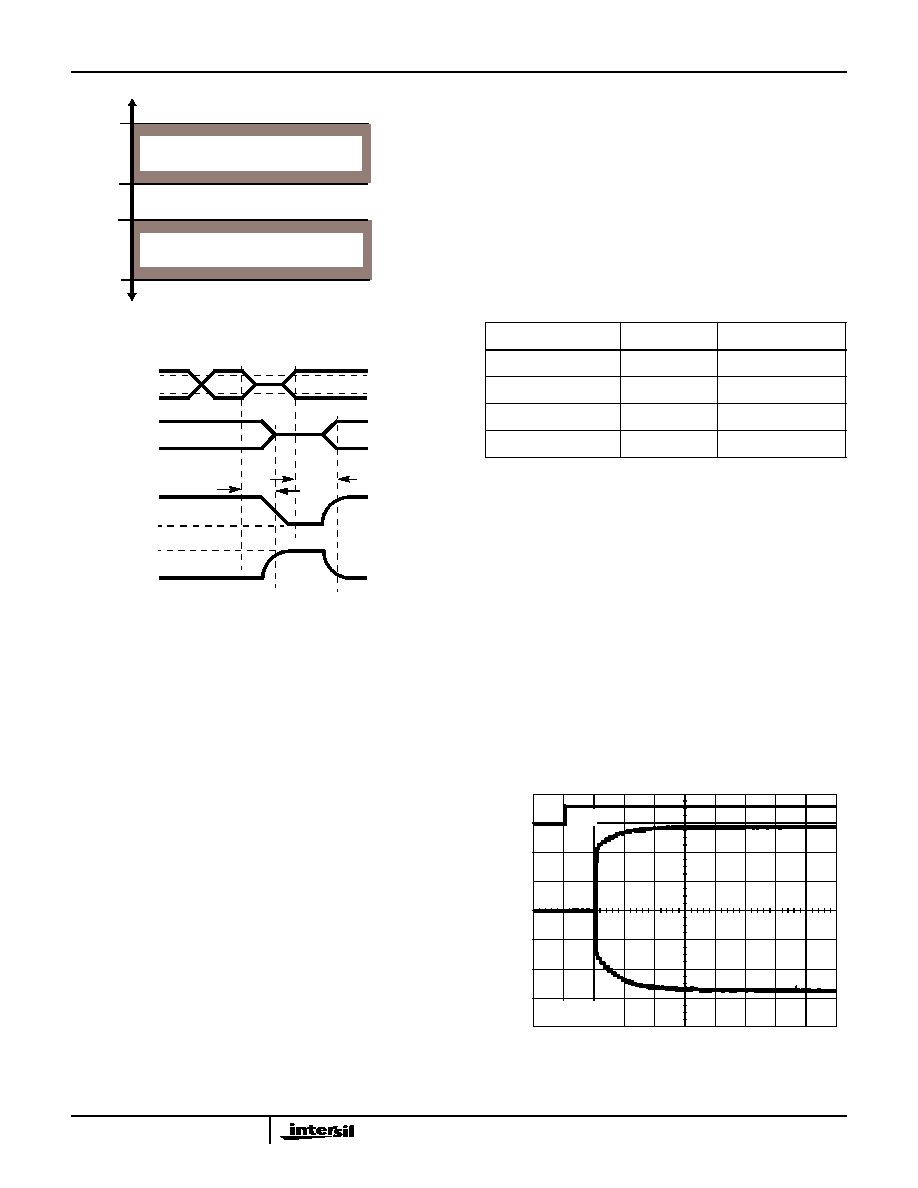
Automatic Powerdown (ICL3217E Only)
Even greater power savings is available by using the
ICL3217E which features an automatic powerdown function.
When no valid RS-232 voltages (see Figure 4) are sensed
on any receiver input for 30
µs, the ICL3217E automatically
enters its powerdown state (see Figure 5). In powerdown,
supply current drops to 1
µA, because the on-chip charge
pump turns off (V+ collapses to V
CC
, V- collapses to GND),
and the receiver and transmitter outputs three-state (see
Table 2). This micro-power mode makes the ICL3217E ideal
for battery powered and portable applications. Invalid
receiver levels occur whenever the driving peripheral's
outputs are shut off (powered down) or when the RS-232
interface cable is disconnected. The ICL3217E powers back
up whenever it detects a valid RS-232 voltage level on any
receiver input (such as when the RS-232 cable is
reconnected). The time to recover from automatic
powerdown mode is typically 100
µs.
R
XOUT
GND
V
ROUT
V
CC
5k
R
XIN
-25V
V
RIN
+25V
GND
V
CC
FIGURE 1. INVERTING RECEIVER CONNECTIONS
FIGURE 2. POWER DRAIN THROUGH POWERED DOWN
PERIPHERAL
OLD
V
CC
POWERED
GND
V
CC
Rx
Tx
V
CC
CURRENT
FLOW
V
OUT
=
V
CC
RS-232 CHIP
DOWN
UART
SHDN = GND
TABLE 2. ICL3217E AUTOMATIC POWERDOWN OPERATION
RS-232 SIGNAL
PRESENT AT
RECEIVER
INPUT?
TRANSMITTER
OUTPUTS
RECEIVER
OUTPUTS
MODE
OF
OPERATION
YES
Active
Active
Normal
Operation
NO
High-Z
High-Z
Powerdown
Due to Auto
Powerdown
Logic
FIGURE 3. DISABLED RECEIVERS PREVENT POWER DRAIN
ICL3217E
TRANSITION
DETECTOR
R
X
T
X
V
CC
V
CC
TO
V
OUT
=
HI-Z*
WAKE-UP
LOGIC
POWERED
DOWN
UART
V-
* IN AUTOMATIC
POWERDOWN
ICL3207E, ICL3217E
6
This automatic powerdown feature provides additional
system power savings without changes to the existing
operating system or hardware.
Utilizing power management circuitry, to power down the rest
of the communication circuitry (e.g., the UART) when the
ICL3217E powers down, produces even greater power
savings. Connecting a transition detector to the V- pin (see
Figure 3) is an easy way for the power management logic to
determine when the ICL3217E enters and exits powerdown.
Capacitor Selection
The charge pumps require 0.1
µF, or greater, capacitors for
3.3V operation. With 0.1
µF capacitors, five percent tolerance
supplies (e.g., 3.14V minimum) deliver greater than
±5V
transmitter swings at full data rate, while ten percent
tolerance supplies (e.g., 2.97V minimum) deliver
±4.95V
transmitter swings. If greater than
±5V transmitter swings are
required with a 10% tolerance 3.3V supply, 0.22
µF
capacitors are recommended (see Table 3). Existing 5V
applications typically utilize either 0.1
µF or 1µF capacitors,
and the ICL32X7E works well with either value. New 5V
designs should use 0.22
µF capacitors for the best results.
For other supply voltages refer to Table 3 for capacitor
values. Do not use values smaller than those listed in
Table 3. Increasing the capacitor values (by a factor of two)
reduces ripple on the transmitter outputs and slightly
reduces power consumption. C
2
, C
3
, and C
4
can be
increased without increasing C
1
's value, however, do not
increase C
1
without also increasing C
2
, C
3
, and C
4
to
maintain the proper ratios (C
1
to the other capacitors).
When using minimum required capacitor values, make sure
that capacitor values do not degrade excessively with
temperature. If in doubt, use capacitors with a larger nominal
value. The capacitor's equivalent series resistance (ESR)
usually rises at low temperatures and it influences the
amount of ripple on V+ and V-
.
Power Supply Decoupling
In most circumstances a 0.1
µF bypass capacitor is
adequate. In applications that are particularly sensitive to
power supply noise, decouple V
CC
to ground with a
capacitor of the same value as the charge-pump capacitor C
1
.
Connect the bypass capacitor as close as possible to the IC.
Transmitter Outputs when Exiting
Powerdown
Figure 6 shows the response of two ICL3217E transmitter
outputs when exiting powerdown mode. As they activate, the
two transmitter outputs properly go to opposite RS-232
levels, with no glitching, ringing, nor undesirable transients.
Each transmitter is loaded with 3k
in parallel with 2500pF.
Note that the transmitters enable only when the magnitude
of the supplies exceed approximately 3V.
.
FIGURE 4. DEFINITION OF VALID RS-232 RECEIVER
LEVELS
0.3V
-0.3V
-2.7V
2.7V
INVALID LEVEL - POWERDOWN OCCURS AFTER 30
µs
VALID RS-232 LEVEL - ICL3217E IS ACTIVE
VALID RS-232 LEVEL - ICL3217E IS ACTIVE
INDETERMINATE - POWERDOWN MAY OR
MAY NOT OCCUR
INDETERMINATE - POWERDOWN MAY OR
MAY NOT OCCUR
RECEIVER
INPUTS
TRANSMITTER
OUTPUTS
V+
V
CC
0
V-
INVALID
REGION
}
FIGURE 5. AUTOMATIC POWERDOWN TIMING DIAGRAM
AUTOPWDN
PWR UP (t
WU
)
TABLE 3. REQUIRED CAPACITOR VALUES
V
CC
(V)
C
1
(
µF)
C
2
, C
3
, C
4
(
µF)
3.15 to 3.6
0.1
0.1
3.0 to 3.6
0.22
0.22
4.5 to 5.5
0.1 to 1.0
0.1 to 1.0
3.0 to 5.5
0.22
0.22
TIME (20
µs/DIV.)
T1
T2
2V/DIV
5V/DIV
V
CC
= +3.3V
C1 - C4 = 0.1
µF
RX
IN
FIGURE 6. TRANSMITTER OUTPUTS WHEN EXITING
POWERDOWN (ICL3217E ONLY)
ICL3207E, ICL3217E
7
Operation down to 2.7V
ICL32X7E transmitter outputs meet RS-562 levels (
±
3.7V)
with V
CC
as low as 2.7V. RS-562 levels typically ensure inter
operability with RS-232 devices.
High Data Rates
The ICL32XX maintain the RS-232
±
5V minimum transmitter
output voltages even at high data rates. Figure 7 details a
transmitter loopback test circuit, and Figure 8 illustrates the
loopback test result at 120kbps. For this test, all transmitters
were simultaneously driving RS-232 loads in parallel with
1000pF, at 120kbps. Figure 9 shows the loopback results for
a single transmitter driving 1000pF and an RS-232 load at
250kbps. The static transmitters were also loaded with an
RS-232 receiver.
Interconnection with 3V and 5V Logic
The ICL32X7E directly interface with 5V CMOS and TTL
logic families. Nevertheless, with the ICL32X7E at 3.3V, and
the logic supply at 5V, AC, HC, and CD4000 outputs can
drive ICL32X7E inputs, but ICL32X7E outputs do not reach
the minimum V
IH
for these logic families. See Table 4 for
more information.
±15kV ESD Protection
All pins on ICL32XX devices include ESD protection
structures, but the ICL32X7E incorporate advanced
structures which allow the RS-232 pins (transmitter outputs
and receiver inputs) to survive ESD events up to
±15kV. The
RS-232 pins are particularly vulnerable to ESD damage
because they typically connect to an exposed port on the
exterior of the finished product. Simply touching the port
pins, or connecting a cable, can cause an ESD event that
might destroy unprotected ICs. These new ESD structures
protect the device whether or not it is powered up, protect
without allowing any latchup mechanism to activate, and
don't interfere with RS-232 signals as large as
±25V.
FIGURE 7. TRANSMITTER LOOPBACK TEST CIRCUIT
FIGURE 8. LOOPBACK TEST AT 120kbps
ICL32X7E
C
1
C
2
C
4
C
3
+
+
+
+
1000pF
V+
V-
5k
T
IN
R
OUT
C1+
C1-
C2+
C2-
R
IN
T
OUT
+
V
CC
0.1
µF
V
CC
T1
IN
T1
OUT
R1
OUT
5
µs/DIV.
V
CC
= +3.3V
5V/DIV.
C1 - C4 = 0.1
µF
FIGURE 9. LOOPBACK TEST AT 250kbps
TABLE 4. LOGIC FAMILY COMPATIBILITY WITH VARIOUS
SUPPLY VOLTAGES
SYSTEM
POWER-
SUPPLY
VOLTAGE
(V)
V
CC
SUPPLY
VOLTAG
E
(V)
COMPATIBILITY
3.3
3.3
Compatible with all CMOS
families.
5
5
Compatible with all TTL and
CMOS logic families.
5
3.3
Compatible with ACT and HCT
CMOS, and with TTL. ICL32X7
E
outputs are incompatible with AC,
HC, and CD4000 CMOS inputs.
T1
IN
T1
OUT
R1
OUT
2
µs/DIV.
5V/DIV.
V
CC
= +3.3V
C1 - C4 = 0.1mF
ICL3207E, ICL3217E

8
Human Body Model (HBM) Testing
As the name implies, this test method emulates the ESD
event delivered to an IC during human handling. The tester
delivers the charge through a 1.5k
current limiting resistor,
making the test less severe than the IEC-1000 test which
utilizes a 330
limiting resistor. The HBM method
determines an ICs ability to withstand the ESD transients
typically present during handling and manufacturing. Due to
the random nature of these events, each pin is tested with
respect to all other pins. The RS-232 pins on "E" family
devices can withstand HBM ESD events to
±15kV.
IEC1000-4-2 Testing
The IEC 1000 test method applies to finished equipment,
rather than to an individual IC. Therefore, the pins most likely
to suffer an ESD event are those that are exposed to the
outside world (the RS-232 pins in this case), and the IC is
tested in its typical application configuration (power applied)
rather than testing each pin-to-pin combination. The lower
current limiting resistor coupled with the larger charge
storage capacitor yields a test that is much more severe than
the HBM test. The extra ESD protection built into this
device's RS-232 pins allows the design of equipment
meeting level 4 criteria without the need for additional board
level protection on the RS-232 port.
AIR-GAP DISCHARGE TEST METHOD
For this test method, a charged probe tip moves toward the
IC pin until the voltage arcs to it. The current waveform
delivered to the IC pin depends on approach speed,
humidity, temperature, etc., so it is difficult to obtain
repeatable results. The "E" device RS-232 pins withstand
±15kV air-gap discharges.
CONTACT DISCHARGE TEST METHOD
During the contact discharge test, the probe contacts the
tested pin before the probe tip is energized, thereby
eliminating the variables associated with the air-gap
discharge. The result is a more repeatable and predictable
test, but equipment limits prevent testing devices at voltages
higher than
±8kV. All "E" family devices survive ±8kV contact
discharges on the RS-232 pins.
Typical Performance Curves
V
CC
= 3.3V, T
A
= 25
o
C
FIGURE 10. TRANSMITTER OUTPUT VOLTAGE vs LOAD
CAPACITANCE
FIGURE 11. SLEW RATE vs LOAD CAPACITANCE
FIGURE 12. SUPPLY CURRENT vs LOAD CAPACITANCE
WHEN TRANSMITTING DATA
FIGURE 13. SUPPLY CURRENT vs SUPPLY VOLTAGE
-6.0
-4.0
-2.0
0
2.0
4.0
6.0
1000
2000
3000
4000
5000
0
LOAD CAPACITANCE (pF)
T
RANS
M
I
T
T
E
R
O
U
T
P
UT
V
O
L
T
A
G
E
(
V
)
1 TRANSMITTER AT 250kbps
V
OUT
+
V
OUT
-
OTHER TRANSMITTERS AT 30kbps
LOAD CAPACITANCE (pF)
SL
EW
R
A
T
E
(
V
/
µ
s)
0
1000
2000
3000
4000
5000
5
10
15
20
25
+SLEW
-SLEW
-SLEW
50
55
15
20
25
30
45
35
40
0
1000
2000
3000
4000
5000
LOAD CAPACITANCE (pF)
S
U
P
P
L
Y
CURRE
NT
(
m
A)
20kbps
250kbps
120kbps
1 TRANSMITTER SWITCHING
S
U
P
P
L
Y
CURRE
NT
(
m
A)
2.5
3.0
3.5
4.0
4.5
5.0
5.5
6.0
0
0.5
1.0
1.5
2.0
SUPPLY VOLTAGE (V)
2.5
3.0
3.5
NO LOAD
ALL OUTPUTS STATIC
ICL3207E, ICL3217E

9
Die Characteristics
DIE DIMENSIONS:
104 mils x 122 mils (2650
µm x 3100µm)
METALLIZATION:
Type: Metal 1: AISi (1%)
Thickness: Metal 1: 8k
≈
Type: Metal 2: AISi (1%)
Thickness: Metal 2: 10k
≈
SUBSTRATE POTENTIAL (POWERED UP):
GND
PASSIVATION:
Type: Silox
Thickness: 13k
≈
TRANSISTOR COUNT:
ICL3207E: 469
ICL3217E: 488
PROCESS:
Si Gate CMOS
ICL3207E, ICL3217E

10
ICL3207E, ICL3217E
11
ICL3207E, ICL3217E
Shrink Small Outline Plastic Packages (SSOP)
NOTES:
1. Symbols are defined in the "MO Series Symbol List" in Section 2.2 of
Publication Number 95.
2. Dimensioning and tolerancing per ANSI Y14.5M-1982.
3. Dimension "D" does not include mold flash, protrusions or gate burrs.
Mold flash, protrusion and gate burrs shall not exceed 0.20mm
(0.0078 inch) per side.
4. Dimension "E" does not include interlead flash or protrusions. Inter-
lead flash and protrusions shall not exceed 0.20mm (0.0078 inch) per
side.
5. The chamfer on the body is optional. If it is not present, a visual index
feature must be located within the crosshatched area.
6. "L" is the length of terminal for soldering to a substrate.
7. "N" is the number of terminal positions.
8. Terminal numbers are shown for reference only.
9. Dimension "B" does not include dambar protrusion. Allowable dambar
protrusion shall be 0.13mm (0.005 inch) total in excess of "B" dimen-
sion at maximum material condition.
10. Controlling dimension: MILLIMETER. Converted inch dimensions
are not necessarily exact.
INDEX
AREA
E
D
N
1
2
3
-B-
0.25(0.010)
C A
M
B S
e
-A-
L
B
M
-C-
A1
A
SEATING PLANE
0.10(0.004)
C
H
µ
0.25(0.010)
B
M
M
0.25
0.010
GAUGE
PLANE
A2
M24.209
(JEDEC MO-150-AG ISSUE B)
24 LEAD SHRINK SMALL OUTLINE PLASTIC PACKAGE
SYMBOL
INCHES
MILLIMETERS
NOTES
MIN
MAX
MIN
MAX
A
-
0.078
-
2.00
-
A1
0.002
-
0.05
-
-
A2
0.065
0.072
1.65
1.85
-
B
0.009
0.014
0.22
0.38
9
C
0.004
0.009
0.09
0.25
-
D
0.312
0.334
7.90
8.50
3
E
0.197
0.220
5.00
5.60
4
e
0.026 BSC
0.65 BSC
-
H
0.292
0.322
7.40
8.20
-
L
0.022
0.037
0.55
0.95
6
N
24
24
7
0
o
8
o
0
o
8
o
-
Rev. 1 3/95

12
All Intersil U.S. products are manufactured, assembled and tested utilizing ISO9000 quality systems.
Intersil Corporation's quality certifications can be viewed at www.intersil.com/design/quality
Intersil products are sold by description only. Intersil Corporation reserves the right to make changes in circuit design, software and/or specifications at any time without
notice. Accordingly, the reader is cautioned to verify that data sheets are current before placing orders. Information furnished by Intersil is believed to be accurate and
reliable. However, no responsibility is assumed by Intersil or its subsidiaries for its use; nor for any infringements of patents or other rights of third parties which may result
from its use. No license is granted by implication or otherwise under any patent or patent rights of Intersil or its subsidiaries.
For information regarding Intersil Corporation and its products, see www.intersil.com
Sales Office Headquarters
NORTH AMERICA
Intersil Corporation
7585 Irvine Center Drive
Suite 100
Irvine, CA 92618
TEL: (949) 341-7000
FAX: (949) 341-7123
Intersil Corporation
2401 Palm Bay Rd.
Palm Bay, FL 32905
TEL: (321) 724-7000
FAX: (321) 724-7946
EUROPE
Intersil Europe Sarl
Ave. William Graisse, 3
1006 Lausanne
Switzerland
TEL: +41 21 6140560
FAX: +41 21 6140579
ASIA
Intersil Corporation
Unit 1804 18/F Guangdong Water Building
83 Austin Road
TST, Kowloon Hong Kong
TEL: +852 2723 6339
FAX: +852 2730 1433
ICL3207E, ICL3217E
Small Outline Plastic Packages (SOIC)
NOTES:
1. Symbols are defined in the "MO Series Symbol List" in Section 2.2 of
Publication Number 95.
2. Dimensioning and tolerancing per ANSI Y14.5M-1982.
3. Dimension "D" does not include mold flash, protrusions or gate burrs.
Mold flash, protrusion and gate burrs shall not exceed 0.15mm
(0.006 inch) per side.
4. Dimension "E" does not include interlead flash or protrusions. Inter-
lead flash and protrusions shall not exceed 0.25mm (0.010 inch) per
side.
5. The chamfer on the body is optional. If it is not present, a visual index
feature must be located within the crosshatched area.
6. "L" is the length of terminal for soldering to a substrate.
7. "N" is the number of terminal positions.
8. Terminal numbers are shown for reference only.
9. The lead width "B", as measured 0.36mm (0.014 inch) or greater
above the seating plane, shall not exceed a maximum value of
0.61mm (0.024 inch)
10. Controlling dimension: MILLIMETER. Converted inch dimensions
are not necessarily exact.
INDEX
AREA
E
D
N
1
2
3
-B-
0.25(0.010)
C A
M
B S
e
-A-
L
B
M
-C-
A1
A
SEATING PLANE
0.10(0.004)
h x 45
o
C
H
µ
0.25(0.010)
B
M
M
M24.3
(JEDEC MS-013-AD ISSUE C)
24 LEAD WIDE BODY SMALL OUTLINE PLASTIC PACKAGE
SYMBOL
INCHES
MILLIMETERS
NOTES
MIN
MAX
MIN
MAX
A
0.0926
0.1043
2.35
2.65
-
A1
0.0040
0.0118
0.10
0.30
-
B
0.013
0.020
0.33
0.51
9
C
0.0091
0.0125
0.23
0.32
-
D
0.5985
0.6141
15.20
15.60
3
E
0.2914
0.2992
7.40
7.60
4
e
0.05 BSC
1.27 BSC
-
H
0.394
0.419
10.00
10.65
-
h
0.010
0.029
0.25
0.75
5
L
0.016
0.050
0.40
1.27
6
N
24
24
7
0
o
8
o
0
o
8
o
-
Rev. 0 12/93