1
Æ
November 2000
ICL7109
12-Bit, Microprocessor-
Compatible A/D Converter
Features
∑ 12-Bit Binary (Plus Polarity and Over-Range) Dual
Slope Integrating Analog-to-Digital Converter
∑ Byte-Organized, TTL Compatible Three-State Outputs
and UART Handshake Mode for Simple Parallel or
Serial Interfacing to Microprocessor Systems
∑ RUN/HOLD Input and STATUS Output Can Be Used to
Monitor and Control Conversion Timing
∑ True Differential Input and Differential Reference
∑ Low Noise (Typ) . . . . . . . . . . . . . . . . . . . . . . . . 15
µV
P-P
∑ Input Current (Typ) . . . . . . . . . . . . . . . . . . . . . . . . . .1pA
∑ Operates At Up to 30 Conversions/s
∑ On-Chip Oscillator Operates with Inexpensive 3.58MHz
TV Crystal Giving 7.5 Conversions/s for 60Hz Rejec-
tion. May Also Be Used with An RC Network Oscillator
for Other Clock Frequencies
Description
The ICL7109 is a high performance, CMOS, low power
integrating A/D converter designed to easily interface with
microprocessors.
The output data (12 bits, polarity and over-range) may be
directly accessed under control of two byte enable inputs and a
chip select input for a single parallel bus interface. A UART
handshake mode is provided to allow the ICL7109 to work with
industry-standard UARTs in providing serial data transmission.
The RUN/HOLD input and STATUS output allow monitoring
and control of conversion timing.
The ICL7109 provides the user with the high accuracy, low
noise, low drift versatility and economy of the dual-slope
integrating A/D converter. Features like true differential input
and reference, drift of less than 1
µV/
o
C, maximum input bias
current of 10pA, and typical power consumption of 20mW
make the ICL7109 an attractive per-channel alternative to
analog multiplexing for many data acquisition applications.
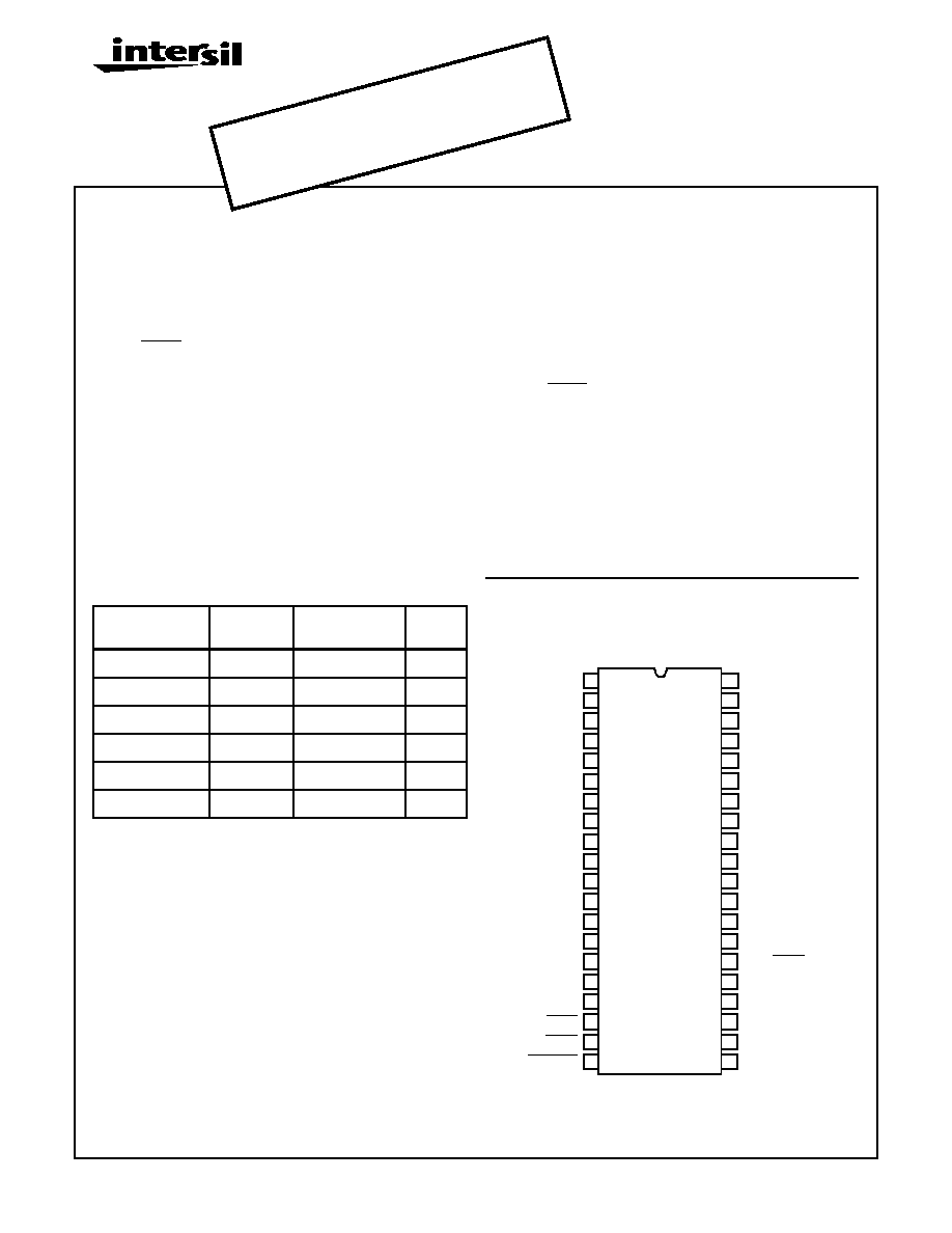
Pinout
ICL7109
(CERDIP, PDIP, SBDIP)
TOP VIEW
Part Number Information
PART NUMBER
TEMP.
RANGE (
o
C)
PACKAGE
PKG.
NO.
ICL7109MDL
-55 to 125
40 Ld SBDIP
D40.6
ICL7109IDL
-25 to 85
40 Ld SBDIP
D40.6
ICL7109IJL
-25 to 85
40 Ld CERDIP
F40.6
ICL7109CPL
0 to 70
40 Ld PDIP
E40.6
ICL7109MDL/883B
-55 to 125
40 Ld SBDIP
D40.6
ICL7109IPL
-25 to 85
40 Ld PDIP
E40.6
13
1
2
3
4
5
6
7
8
9
10
11
12
14
15
16
17
18
19
20
GND
STATUS
POL
OR
B12
B11
B10
B9
B8
B7
B6
B5
B4
B3
B2
B1
TEST
LBEN
HBEN
CE/LOAD
28
40
39
38
37
36
35
34
33
32
31
30
29
27
26
25
24
23
22
21
V+
REF IN -
REF CAP-
REF CAP+
REF IN+
IN HI
IN LO
COMMON
INT
AZ
BUF
REF OUT
V-
SEND
RUN/HOLD
BUF OSC OUT
OSC SEL
OSC OUT
OSC IN
MODE
File Number
3092.2
CAUTION: These devices are sensitive to electrostatic discharge; follow proper IC Handling Procedures.
1-888-INTERSIL or 321-724-7143
|
Intersil (and design) is a registered trademark of Intersil Americas Inc.
Copyright © Intersil Americas Inc. 2002. All Rights Reserved
FOR
A PO
SSIB
LE S
UBST
ITUT
E PR
ODU
CT
conta
ct ou
r Tec
hnica
l Sup
port
Cent
er at
1-888
-INTE
RSIL
or w
ww.in
tersil
.com
/tsc
OBSO
LETE
PRO
DUCT

2
Absolute Maximum Ratings
Thermal Information
Positive Supply Voltage (GND to V+). . . . . . . . . . . . . . . . . . . . +6.0V
Negative Supply Voltage (GND to V-) . . . . . . . . . . . . . . . . . . . . . -9V
Analog Input Voltage (Either Input) (Note 1) . . . . . . . . . . . . V+ to V-
Reference Input Voltage (Either Input) (Note 1) . . . . . . . . . . V+ to V-
Digital Input Voltage . . . . . . . . . . . . . . . . . . . . . . . . . . . . . (V+) +0.3V
Pins 2-27 (Note 2) . . . . . . . . . . . . . . . . . . . . . . . . . . . . . . GND -0.3V
Operating Conditions
Temperature Range
M Suffix. . . . . . . . . . . . . . . . . . . . . . . . . . . . . . . . . -55
o
C to 125
o
C
I Suffix . . . . . . . . . . . . . . . . . . . . . . . . . . . . . . . . . . . -25
o
C to 85
o
C
C Suffix . . . . . . . . . . . . . . . . . . . . . . . . . . . . . . . . . . . .0
o
C to 75
o
C
Thermal Resistance (Typical, Note 1)
JA
(
o
C/W)
JC
(
o
C/W)
SBDIP Package. . . . . . . . . . . . . . . . . . . .
60
20
CERDIP Package . . . . . . . . . . . . . . . . . .
55
18
PDIP Package . . . . . . . . . . . . . . . . . . . . .
50
N/A
Maximum Junction Temperature (PDIP Package) . . . . . . . . . 150
o
C
Maximum Junction Temperature (CERDIP Package). . . . . . . 175
o
C
Maximum Storage Temperature Range . . . . . . . . . . -65
o
C to 150
o
C
Maximum Lead Temperature (Soldering 10s Max). . . . . . . . . 300
o
C
CAUTION: Stresses above those listed in "Absolute Maximum Ratings" may cause permanent damage to the device. This is a stress only rating and operation
of the device at these or any other conditions above those indicated in the operational sections of this specification is not implied.
NOTE:
1.
JA
is measured with the component mounted on an evaluation PC board in free air.
Analog Electrical Specifications
V+ = +5V, V- = -5V, GND = 0V, T
A
= 25
o
C, f
CLK
= 3.58MHz,
Unless Otherwise Specified
PARAMETER
TEST CONDITIONS
MIN
TYP
MAX
UNIT
SYSTEM PERFORMANCE
Oscillator Output Current
High, O
OH
V
OUT
= 2.5V
-
1
-
mA
Low, O
OL
V
OUT
= 2.5V
-
1.5
-
mA
Buffered Oscillator Output Current
High, BO
OH
V
OUT
= 2.5V
-
2
-
mA
Low, BO
OL
V
OUT
= 2.5V
-
5
-
mA
Zero Input Reading
V
IN
= 0.0000V, V
REF
= 204.8mV
-0000
±0000
+0000
Counts
Ratiometric Error
V
lN
= V
REF
, V
REF
= 204.8mV (Note 7)
-3
-
0
Counts
Non-Linearity
Full Scale = 409.6mV to 2.048mV
Maximum Deviation from Best Straight Line Fit, Over
Full Operating Temperature Range (Notes 4 and 6)
-1
±0.2
+1
Counts
Rollover Error
Full Scale = 409.6mV to 2.048V
Difference in Reading for Equal Positive and Negative
Inputs Near Full Scale (Notes 5 and 6), R
1
= 0
-1
±0.2
+1
Counts
Linearity
Full-Scale = 200mV or Full Scale = 2V Maximum
Deviation from Best Straight Line Fit (Note 4)
-
±0.2
±1
Counts
Common Mode Rejection Ratio, CMRR V
CM
=
±1V, V
IN
= 0V, Full Scale = 409.6mV
-
50
-
µV/V
Input Common Mode Range, VCMR
Input HI, Input LO, Common (Note 4)
(V-)
+2.0
-
(V+)
-2.0
V
Noise, eN
V
IN
= 0V, Full-Scale = 409.6mV
(Peak-to-Peak Value Not Exceeded 95% of Time)
-
15
-
µV
Leakage Current Input, I
ILK
V
lN
= 0V, All Devices at 25
o
C (Note 4)
-
1
10
pA
ICL7109CPL 0
o
C to 70
o
C (Note 4)
-
20
100
pA
ICL7109IDL
-25
o
C to 85
o
C (Note 4)
-
100
250
pA
ICL7109MDL
-55
o
C to 125
o
C
-
2
100
nA
Zero Reading Drift
V
lN
= 0V, R
1
- 0
(Note 4)
-
0.2
1
µV/
o
C
ICL7109
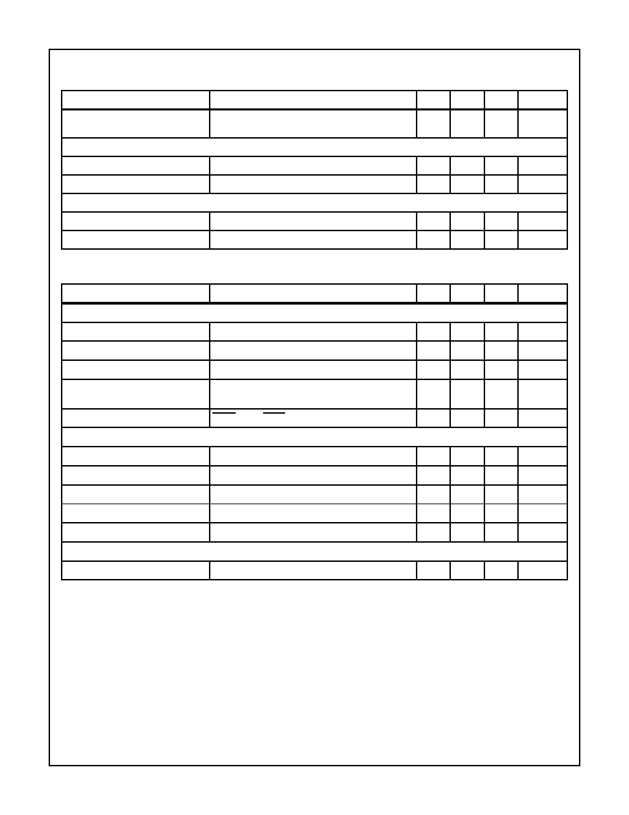
3
Scale Factor Temperature Coefficient
V
IN
= 408.9mV = > 7770
8
Reading Ext. Ref. 0ppm/
o
C
(Note 4)
-
1
5
ppm/
o
C
REFERENCE VOLTAGE
Ref Out Voltage, V
REF
Referred to V+, 25k
Between V+ and REF OUT
-2.4
-2.8
-3.2
V
Ref Out Temperature Coefficient
25k
Between V+ and REF OUT (Note 4)
-
80
-
ppm/
o
C
POWER SUPPLY CHARACTERISTICS
Supply Current V+ to GND, I+
V
IN
= 0V, Crystal Osc 3.58MHz Test Circuit
-
700
1500
µA
Supply Current V+ to V-, I
SUPP
Pins 2 - 21, 25, 26, 27, 29; Open
-
700
1500
µA
Digital Electrical Specifications
V+ = +5V, V- = -5V, GND = 0V, T
A
= 25
o
C, Unless Otherwise Specified
PARAMETER
TEST CONDITIONS
MIN
TYP
MAX
UNIT
DIGITAL OUTPUTS
Output High Voltage, V
OH
I
OUT
= 100
µA Pins 2 - 16, 18, 19, 20
3.5
4.3
-
V
Output Low Voltage, V
OL
I
OUT
= 1.6mA Pins 2 - 16, 18, 19, 20
-
±0.20
±0.40
V
Output Leakage Current
Pins 3 - 16 High Impedance
-
±0.01
±1
µA
Control I/O Pullup Current
Pins 18, 19, 20 V
OUT
= V+ -3V MODE Input at GND
(Note 4)
-
5
-
µA
Control I/O Loading
HBEN Pin 19 LBEN Pin 18 (Note 4)
-
-
50
pF
DIGITAL INPUTS
Input High Voltage, V
IH
Pins 18 - 21, 26, 27 Referred to GND
3.0
-
-
V
Input Low Voltage, V
IL
Pins 18 - 21, 26, 27 Referred to GND
-
-
1
V
Input Pull-Up Current
Pins 26, 27 V
OUT
= (V+) -3V
-
5
-
µA
Input Pull-Up Current
Pins 17, 24 V
OUT
= (V+) -3V
-
25
-
µA
Input Pull-Down Current
Pin 21 V
OUT
= GND +3V
-
5
-
µA
TIMING CHARACTERISTICS
MODE Input Pulse Width, t
W
(Note 4)
50
-
-
ns
NOTES:
1. Input voltages may exceed the supply voltages provided the input current is limited to
±100µA.
2. Due to the SCR structure inherent in the process used to fabricate these devices, connecting any digital inputs or outputs to voltages
greater than V+ or less than GND may cause destructive device latchup. For this reason it is recommended that no inputs from sources
other than the same power supply be applied to the ICL7109 before its power supply is established, and that in multiple supply systems
the supply to the ICL7109 be activated first.
3. This limit refers to that of the package and will not be obtained during normal operation.
4. This parameter is not production tested, but is guaranteed by design.
5. Roll-over error for T
A
= -55
o
C to 125
o
C is
±10 counts (Max).
6. A full scale voltage of 2.048V is used because a full scale voltage of 4.096V exceeds the devices Common Mode Voltage Range.
7. For CERDIP package the Ratiometric error can be -4 (Min).
Analog Electrical Specifications
V+ = +5V, V- = -5V, GND = 0V, T
A
= 25
o
C, f
CLK
= 3.58MHz,
Unless Otherwise Specified (Continued)
PARAMETER
TEST CONDITIONS
MIN
TYP
MAX
UNIT
ICL7109
4
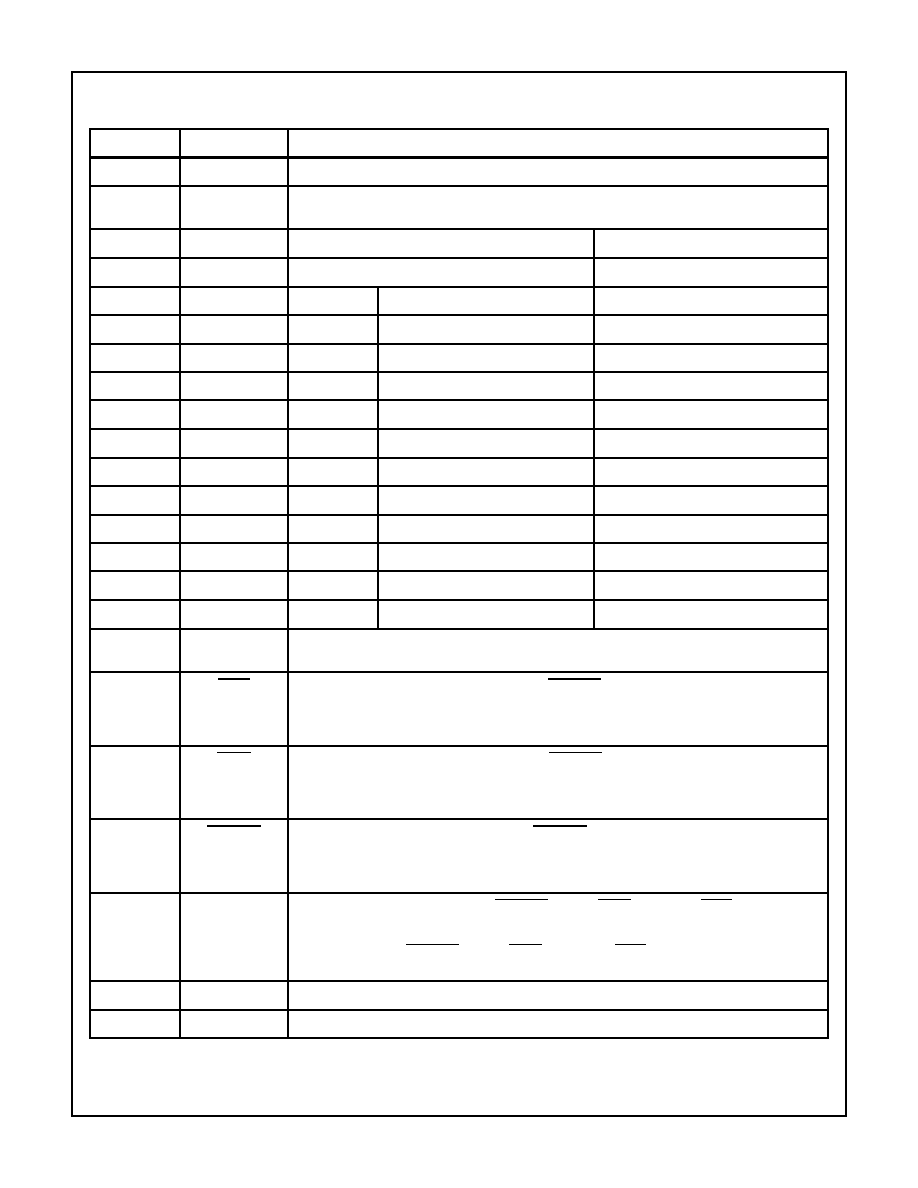
Pin Descriptions
PIN
SYMBOL
DESCRIPTION
1
GND
Digital Ground, 0V. Ground return for all digital logic.
2
STATUS
Output High during integrate and deintegrate until data is latched. Output Low when analog section
is in Auto-Zero configuration.
3
POL
Polarity - HI for positive input.
Three-State Output Data Bits
4
OR
Overrange - HI if overranged.
Three-State Output Data Bits
5
B12
Bit 12
(Most Significant Bit)
Three-State Output Data Bits
6
B11
Bit 11
High = True
Three-State Output Data Bits
7
B10
Bit 10
High = True
Three-State Output Data Bits
8
B9
Bit 9
High = True
Three-State Output Data Bits
9
B8
Bit 8
High = True
Three-State Output Data Bits
10
B7
Bit 7
High = True
Three-State Output Data Bits
11
B6
Bit 6
High = True
Three-State Output Data Bits
12
B5
Bit 5
High = True
Three-State Output Data Bits
13
B4
Bit 4
High = True
Three-State Output Data Bits
14
B3
Bit 3
High = True
Three-State Output Data Bits
15
B2
Bit 2
High = True
Three-State Output Data Bits
16
B1
Bit 1
(Least Significant Bit)
Three-State Output Data Bits
17
TEST
Input High - Normal Operation. Input Low - Forces all bit outputs high. Note: This input is used for
test purposes only. Tie high if not used.
18
LBEN
Low Byte Enable - With Mode (Pin 21) low, and CE/LOAD (Pin 20) low, taking this pin low activates
low order byte outputs B1 through B8.
With Mode (Pin 21) high, this pin serves as a low byte flag output used in handshake mode.
See Figures 7, 8, 9.
19
HBEN
High Byte Enable - With Mode (Pin 21) low, and CE/LOAD (Pin 20) low, taking this pin low activates
high order byte outputs B9 through B12, POL, OR.
With Mode (Pin 21) high, this pin serves as a high byte flag output used in handshake mode.
See Figures 7, 8, 9.
20
CE/LOAD
Chip Enable Load - With Mode (Pin 21) low. CE/LOAD serves as a master output enable. When
high, B1 through B12, POL, OR outputs are disabled.
With Mode (Pin 21) high, this pin serves as a load strobe used in handshake mode.
See Figures 7, 8, 9.
21
MODE
Input Low - Direct output mode where CE/LOAD (Pin 20), HBEN (Pin 19) and LBEN (Pin 18) act as
inputs directly controlling byte outputs.
Input Pulsed High - Causes immediate entry into handshake mode and output of data as in Figure 9.
Input High - Enables CE/LOAD (Pin 20), HBEN (Pin 19), and LBEN (Pin 18) as outputs, handshake
mode will be entered and data output as in Figures 7 and 8 at conversion completion.
22
OSC IN
Oscillator Input
23
OSC OUT
Oscillator Output
ICL7109

5
24
OSC SEL
Oscillator Select - Input high configures OSC IN, OSC OUT, BUF OSC OUT as RC oscillator - clock
will be same phase and duty cycle as BUF OSC OUT.
Input low configures OSC IN, OSC OUT for crystal oscillator - clock frequency will be 1/58 of
frequency at BUF OSC OUT.
25
BUF OSC OUT
Buffered Oscillator Output
26
RUN/HOLD
Input High - Conversions continuously performed every 8192 clock pulses.
Input Low - Conversion in progress completed, converter will stop in Auto-Zero 7 counts before
integrate.
27
SEND
Input - Used in handshake mode to indicate ability of an external device to accept data. Connect to
+5V if not used.
28
V-
Analog Negative Supply - Nominally -5V with respect to GND (Pin 1).
29
REF OUT
Reference Voltage Output - Nominally 2.8V down from V+ (Pin 40).
30
BUFFER
Buffer Amplifier Output.
31
AUTO-ZERO
Auto-Zero Node - Inside foil of C
AZ
.
32
INTEGRATOR
Integrator Output - Outside foil of C
INT
.
33
COMMON
Analog Common - System is Auto-Zeroed to COMMON.
34
INPUT LO
Differential Input Low Side.
35
INPUT HI
Differential Input High Side.
36
REF IN +
Differential Reference Input Positive.
37
REF CAP +
Reference Capacitor Positive.
38
REF CAP-
Reference Capacitor Negative.
39
REF IN-
Differential Reference Input Negative.
40
V+
Positive Supply Voltage - Nominally +5V with respect to GND (Pin 1).
NOTE: All digital levels are positive true.
Pin Descriptions
(Continued)
PIN
SYMBOL
DESCRIPTION
ICL7109