
1
Æ
October 1997
ICL7121
16-Bit Multiplying
Microprocessor-Compatible D/A Converter
Features
∑ 16-Bit Resolution
∑ Low Integral Linearity Error -0.003% FSR
∑ Monotonic to 16 Bits Over Full Military Temperature
Range (LM Grade)
∑ Microprocessor Compatible with Buffered Inputs
∑ Bipolar Application Requires No External Resistors
∑ Output Current Settling Time 3
µs Max (1µs Typ)
∑ Low Linerarity and Gain Temperature Coefficients
∑ Low Power Dissipation (25mW)
∑ Full Four-Quadrant Multiplication
∑ Low Differential Nonlinearity Error at Bipolor Zero
Description
The ICL7121 achieves 0.003% linearity without laser
trimming by combining a four quadrant multiplying DAC
using thin film resistors with an on-chip PROM-controlled
correction circuit. Silicon-gate CMOS circuitry keeps the
power dissipation very low.
Microprocessor bus interfacing is eased using standard
memory WRITE cycle timing and control. The input buffer
register is loaded with the 16-bit input and directly controls
the output switches. The register is transparent if WR and
CS are held low.
The ICL7121 is designed and programmed for bipolar
operation. There is an offset resistor to the output which
should be connected to -V
REF
and an inverter on the MSB
line, giving the DAC a 2's complement bipolar transfer
function. Two extra resistors are included on the chip to
facilitate the reference inversion, so that only an external op-
amp is needed.
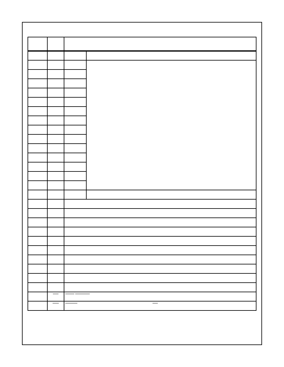
Pinout
ICL7121
(OUTLINE DWG JI)
TOP VIEW
Ordering Information
PART NUMBER
TEMP. RANGE
(
o
C)
PACKAGE
ICL7121JCJI
0 to 70
28 Ld CERDIP
ICL7121JMJI
-55 to 125
28 Ld CERDIP
ICL7121KCJI
0 to 70
28 Ld CERDIP
ICL7121KMJI
-55 to 125
28 Ld CERDIP
ICL7121LCJI
0 to 70
28 Ld CERDIP
ICL7121LMJI
-55 to 125
28 Ld CERDIP
28
27
26
25
24
23
22
21
20
19
18
17
16
15
(LSB) D
0
D
1
D
2
D
3
D
4
D
5
D
6
D
7
D
8
D
9
D
10
D
11
1
2
3
4
5
6
7
8
9
10
11
12
13
14
CS
V+
I
OUT
AGND
S
AGND
F
R
FB
R
INV
V
REF
PROG
D
15
(MSB)
D
14
WR
DGND
R
OFS
D
12
D
13
CAUTION: These devices are sensitive to electrostatic discharge; follow proper IC Handling Procedures.
1-888-INTERSIL or 321-724-7143
|
Intersil (and design) is a registered trademark of Intersil Americas Inc.
Copyright © Intersil Americas Inc. 2002. All Rights Reserved
File Number
3112.1
NOT
REC
OMM
END
ED F
OR N
EW D
ESIG
NS

2
Functional Block Diagram
ICL7121
3
Pin Descriptions
28 LEAD
CERDIP
PIN
NAME
PIN DESCRIPTION
1
D
0
Bit 0
Least Significant
2
D
1
Bit1
Input Data Bits (High = True)
3
D
2
Bit 2
4
D
3
Bit 3
5
D
4
Bit 4
6
D
5
Bit 5
7
D
6
Bit 6
8
D
7
Bit 7
9
D
8
Bit 8
10
D
9
Bit 9
11
D
10
Bit 10
12
D
11
Bit 11
13
D
12
Bit 12
14
D
13
Bit 13
15
D
14
Bit 14
16
D
15
Bit 15
Most significant
17
PROG
Used for programming only. Tie to +5V for normal operation.
18
V
REF
V
REF
input to ladder.
19
R
INV
Summing node for reference inverting amplifier.
20
R
OFS
Bipolar offset resistor, to -V
REF
.
21
R
FB
Feedback resistor for voltage output applications.
22
DGND
Digital Ground Return.
23
AGND
F
Analog Ground force lines. Use to carry current from internal Analog GND connections.
24
AGND
S
Analog Ground sense line. Reference point for external circuitry. Pin should carry minimal current.
25
I
OUT
Current output pin.
26
V+
Positive Supply.
27
CS
CHIP SELECT (active low). Enables register write.
28
WR
WRITE, (active low). Writes in register. Equivalent to CS.
ICL7121
4
Absolute Maximum Ratings
(Note 1)
Thermal Information
Supply Voltage (V+ to DGND) . . . . . . . . . . . . . . . . . . . -0.3V to 7.5V
V
RFL
, R
OFS
, R
INV
, R
FB
to DGND
. . . . . . . . . . . . . . . . . . . . . . . . ±25V
Current in AGND
S
, AGND
F
. . . . . . . . . . . . . . . . . . . . . . . . . . . 25mA
D
N
, WR, CS, PROG, I
OUT
, AGND
S
, AGND
F
. . . -0.3V to V+ +0.3V
Operating Conditions
Temperature Range
ICL7121C . . . . . . . . . . . . . . . . . . . . . . . . . . . . . . . . . .0
o
C to 70
o
C
ICL7121M . . . . . . . . . . . . . . . . . . . . . . . . . . . . . . . -55
o
C to 125
o
C
Storage Temperature Range . . . . . . . . . . . . . . . . . .-65
o
C to 150
o
C
Power Dissipation (Note 2) . . . . . . . . . . . . . . . . . . . . . . . . . . 500mW
Derate Linearly Above 70
o
C @10mW/
o
C
Lead Temperature (Soldering, 10s) . . . . . . . . . . . . . . . . . . . . 300
o
C
CAUTION: Stresses above those listed in "Absolute Maximum Ratings" may cause permanent damage to the device. This is a stress only rating and operation
of the device at these or any other conditions above those indicated in the operational sections of this specification is not implied.
NOTES:
1. All voltages with respect to DGND.
2. Assumes all leads soldered or welded to printed circuit board.
Electrical Specifications
V+ = +5V, V
REF
= +5V, T
A
= 25
o
C, AGND = DGND, I
OUT
at Ground Potential,
Unless Otherwise Specified
PARAMETER
TEST CONDITIONS
MIN
TYP
MAX
UNITS
DC ACCURACY
Resolution
16
-
-
Bits
Monotonicity
Guaranteed by DLE Test (Note 3)
J
14
-
-
Bits
K
15
-
-
Bits
L
16
-
-
Bits
Differential Linearity Error at
Bipolar Zero
T
A
= 25
o
C
J, K
-
-
±1
LSB
L
-
-
±1/2
LSB
Operating Temperature Range
J, K
-
-
±11/2
LSB
L
-
-
±1
LSB
Differntial Linearity Error DLE
T
A
= 25
o
C
J
-
-
±0.006
%FSR
K
-
-
±0.003
%FSR
L
-
-
+0.003
-0.0015
%FSR
Operating Temperature Range
J,KC
-
-
±0.006
%FSR
LC, KM
-
-
+0.0045
-0.003
%FSR
LM
-
-
+0.0045
-0.0015
%FSR
Integral Linearity Error ILE
T
A
= 25
o
C
J
-
±0.003
±0.006
%FSR
K,L
-
±0.0015
±0.003
%FSR
Operating Temperature Range
J
-
±0.006
±0.009
%FSR
K, LM
-
±0.003
±0.006
%FSR
LC
-
±0.0015
±0.003
%FSR
Integral Linearity Error
Temperature Coefficient
J
-
±0.3
±1.2
ppm/
o
C
K,L
-
±0.2
±0.9
ppm/
o
C
ICL7121
5
Unadjusted Gain Error
T
A
= 25
o
C
J
-
±0.004
±0.012
%FSR
K
-
±0.003
±0.009
%FSR
L
-
±0.002
±0.006
%FSR
Operating Temperature Range
J
-
±0.002
+0.04
%FSR
K, L
-
±0.01
±0.02
%FSR
Unadjusted Gain Error
Temperature Coefficient
(Note 4)
J
-
±1.0
±5.2
ppm/
o
C
K, L
-
±0.5
±2.0
ppm/
o
C
Unadjusted Output Offset
DAC Register Outputs All LOW (Note 6)
-
±4
±15
mV
Output Offset Temperature Drift
Same Conditions as Above, (Note 4)
-
-
±5
µV/
o
C
AC ACCURACY
Power Supply Rejection
V+ = 5V ±10%, T
A
= 25
o
C
-
±30
±100
ppm/C
Operating Temperature Range
-
±50
±150
ppm/C
Output Current Settling Time
To 1/2 LSB (Note 4)
-
1.8
3
µs
REFERENCE INPUT
Input Resistance
I
OUT
at Ground
3
4.2
6
k
ANALOG OUTPUT
Output Capacitance
(I
OUT
Terminal)
DAC Register Outputs All Low
-
150
-
pF
DAC Register Outputs All High
-
300
-
pF
DIGITAL INPUTS
LOW State Threshold
Operating Temperature Range
-
-
0.8
V
HIGH State Threshold
2.4
-
-
V
Input Current
Inputs Between DGND to V+
-
±0.001
±1
µA
Input Capacitance
(Note 4)
-
15
-
pF
POWER SUPPLY
Supply Voltage Rnage *
Functional Operation (Note 5)
4.5
-
5.5
V
Supply Current
(Excluding Ladder Network)
T
A
= 25
o
C, Digital Inputs High or LOW
-
0.6
1.5
mA
Operating Temperature Range Digital Inputs
HIGH or LOW
-
1.0
2.5
mA
NOTES:
3. Military temperature range parts are also tested to stated limits at -55
o
C and 125
o
C.
4. Guaranteed by characterization but not tested on a production basis.
5. Guaranteed by PSRR test.
6. Refer to FIgure 1. Measured at output amplifier A1 (A1 having zero offset). V
REF
= +5V. Adjustable to zero with external potentiometer.
Switching Specifications
V+ = 5V, T
A
= 25
o
C, See Timing Diagram
PARAMETER
SYMBOL
TEST CONDITIONS
MIN
TYP
MAX
UNITS
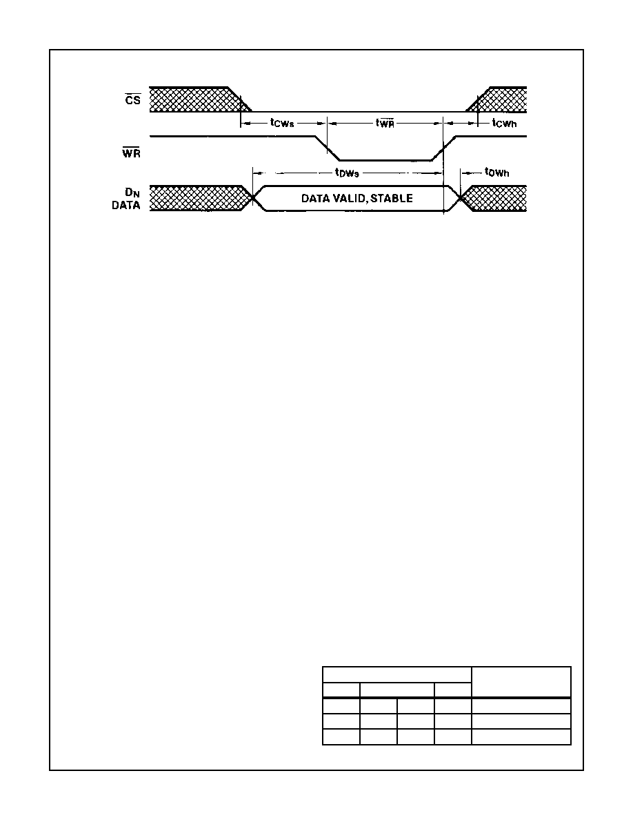
CHIP SELECT-WRITE Set-Up Time
t
CWs
Note 4
0
-
-
ns
CHIP SELECT-WRITE Hold Time
t
CWh
Note 4
0
-
-
ns
WRITE Pulse Width Low
t
WR
Note 4
200
-
-
ns
Data-WRITE Set-Up Time
t
DWs
Note 4
200
-
-
ns
Data-WRITE Hold Time
t
DWh
Note 4
0
-
-
ns
Electrical Specifications
V+ = +5V, V
REF
= +5V, T
A
= 25
o
C, AGND = DGND, I
OUT
at Ground Potential,
Unless Otherwise Specified (Continued)
PARAMETER
TEST CONDITIONS
MIN
TYP
MAX
UNITS
ICL7121

6
Test Circuits
FIGURE 1. BIPOLAR OPERATION, FOUR-QUADRANT
FIGURE 2. BIPOLAR OPERATION WITH FORCED GROUND
ICL7121
7
Definition of Terms
Integral Linerarity Error - Error contributed by deviation of
the DAC transfer function from a "best staight line" through
the actual plot of transfer function. Normally expressed as a
percentage of full scale range or in (sub)multiples of 1 LSB.
Differential Linearity Error - The difference between ideal
and actual value of the analog output "step size" for any two
adjacent digital input code. The ideal "step size" is equal to
2
-n
of full scale for an n-bit DAC or 1 LSB. It is expressed in
(sub)multiples of 1 LSB.
Resolution - It is addressing the smallest distinct analog
output change that a D/A converter can produce. It is
commonly expressed as the number of converter bits. A
converter with resolution of n bits can resolve output
changes of 2
-n
of the full-scale range, e.g. 2
-n
V
REF
for a
unipolar conversion. Resolution by no means implies
linearity.
Settling Time - Time required for the output of a DAC to
settle to within a specified error band around its final value
(e.g. 1/2 LSB) for a given digital input change, i.e., all digital
inputs LOW to HIGH and HIGH to LOW.
Gain Error - The difference between actual and ideal analog
output values at full-scale range, ie.e. all digital inputs at
HIGH state. It is expressed as a percentage of full-scale
range or in (sub)multiples of 1 LBB.
Output Capacitance - Capcitance from I
OUT
terminal to
ground.
Detailed Description
The ICL7121 consists of a 16-bit primary DAC, PROM con-
trolled correction DACs, input buffer registers, and micropro-
cessor interface logic. The 16-bit primary DAC is an R-2R
thin film resistor ladder with N-channel MOS SPDT current
steering switches. Precise balancing of the switch resis-
tances and all other resistors in the ladder results in excel-
lent temperature stability.
The low linearity error is achieved by programming a floating
polysilicon gate PROM array which controls a 12-bit correc-
tion DAC (C-DAC). The most significant bits of the primary
DAC register address this PROM array. Thus for every com-
bination of the primary DAC's most significant bits a different
C-DAC code is selected, allowing correctino of superposition
erros. These errors are cuased by bit interaction on the pri-
mary ladder's current bus and by voltage non-linearity in the
feedback resistor. Superposition errors cannot be corrected
by any method that corrects individual bits only, such as
laser trimming.
The onboard PROM also controls the 6-bit gain DAC. The G-
DAC reduces gain error to less than 0.006% FSR by divert-
ing to analog ground up to 2% of the current flowing in R
FB
.
Since the PROM programming occurs in packaged form, it
corrects for resistor shifts caused by the thermal stresses of
packaging, unlike wafer-level trimming methods. Also, since
the thin film resistors do not suffer laser trimming stresses,
no degradation of time-stability results.
Applications
Bipolar Operation
The circuit diagram for the normal configuration of the
ICL7121 is shown in Figure 1. The positive and negative
reference voltages allow full four-qudrant multiplication.
Amplifier A
3
, together with the internal resistors R
INV1
and
R
INV2
, forms a simple voltage inverter circuit to generate -
V
REF
for the R
OFS
offset input pin. This will give the nominal
"digital input code/analog otuput value" relationship of Table
1. Note that the value of R
FB
is equal to 2R so full scale
range is 2V
REF
.
The offset binary transfer function can be achieved simply by
inverting the MSB. Inversion of the MSB can be done by an
inverter or may be done in software.
Timing Diagram
FIGURE 3.
TABLE 1. 2'S COMPLEMENT BIPOLAR OPERATION
DIGITAL INPUT
ANALOG OUTPUT
MSB
LSB
0111
1111
1111
1111
-V
REF
(1 - 1/2
15
)
0111
1111
1111
1110
-V
REF
(1 - 1/2
14
)
0000
0000
0000
0001
-V
REF
(1/2
15
)
ICL7121
8
Amplifier A
1
is the output amplifier. An additional amplifier
A
2
may be used to force AGND
F
if the ground reference
piont is established elsewhere that at the DAC, as in Figure
2.
A feedback compensation capacitor, C
F
, improves the
settling time by reducing ringing. This capacitor is normally in
the 10pF - 40pF range, depending on layout and the output
amplifier selected. If C
F
is too small, rigning or oscillation
can occur when using an op amp with a high gain
bandwidth. If C
F
is too large, the response of the output
amplifier will be overdamped and will settle slowly.
The input circuits of some high speed op amps will sink large
currents to their negative supply during power up and power
down. The Schottky diode at I
OUT
limits any negative-going
transitions to less than -0.4V, avoiding the SCR latchup
which could result if significant current was injected into the
parasitic diode between I
OUT
and DGND of the ICL7121.
This diode is not needed when using the ICL7650 ultra low
V
OS
op amp.
Digital Interface
The ICL7121 has a 16-bit latch onboard and can interface
directly to a 16-bit data bus. As shown in Figure 4, external
latches or peripheral ICs can be used to interface to an 8-bit
data bus. To ensure that the data is written into the onboard
latch, the data must be valid 200ns before the rising edge of
WR. If WR and CS are both low, the onboard latch is
transparent and the input data is directly applied to the
internal R-2R ladder switches. While this simplifies
interfacing in non-microprocessor systems, having WR low
before data is valid may cause additional glitchews in some
microprocessor systems. To avoid these glitches, data must
be valid at the time WR goes low.
All digital interfaces can suffer from capacitive coupling
between the digital lines and the analog section. There are
two general precautions that will reduce this capacitive
coupling problem: 1) reduce stray capacitance between
digital lines and analog lines; and 2) reduce the number of
transitions on the digital inputs. Careful board layout and
shielding can minimize the capacitive coupling (see Figure
5). The activity on the digital input lines can be reduced by
using external latches or peripheral interface ICs between
the microprocessor bus and the ICL7121. This will reduce
the number of transitions on the digital data and control lines
of the ICL7121, thereby reducing the amount of digital noise
coupled into the sensitve analog sections.
0000
0000
0000
0000
0
1111
1111
1111
1111
+V
REF
(1/2
15
)
1000
0000
0000
0010
+V
REF
(1 - 1/2
14
)
1000
0000
0000
0001
+V
REF
(1 - 1/2
15
)
1000
0000
0000
0000
+V
REF
TABLE 1. 2'S COMPLEMENT BIPOLAR OPERATION
DIGITAL INPUT
ANALOG OUTPUT
MSB
LSB
FIGURE 4. INTERFACE TO 8-BIT MICROPROCESSOR
ICL7121

9
FIGURE 5A. PRINTED CIRCUIT SIDE OF BOARD
FIGURE 5B. TOP SIDE WITH COMPONENT PLACEMENT
FIGURE 5. PRINTED CIRCUIT BOARD LAYOUT (SINGLE SIDED BOARD)
ICL7121
10
Operational Amplifier Section
The input offset voltage, input current, gain, and bandwidth
of the op amps used affect the circuit performance. Since the
output impedance of I
OUT
varies with the digital input code,
the input current of amplifier A
1
will cause a code-dependent
error at V
OUT
, degrading the linearity. The input bias current
should be significantly less than 1 LSB current, which is
about 10nA. In a similar manner, any offset voltage in A
1
will
cause linearity errors. The offset voltage of the output
amplifier should be significantly less than 1 LSB (153
µV at
V
REF
= 5V).
The voltage output setting time is highly dependent on the
slew rate and gain-bandwidth of A
1
, so for high speed
operation a high speed op amp such as the HA2600 is
recommended. For applications where high speed is not
required, the ICL7650 or ICL7652 can be used for A
1
. Since
the ICL7650/52 offset voltage is less than 5
µV, no offset
trimming is needed. To get a full 5V output swing from these
op amps,
±7.5V supplies should be used for the ICL7650/52.
Amplifer A
3
, which is used to generate the inverted
reference, needs only to have a stable offset and to be able
to drive a 3k
load. Since this is strictly a DC amplifier, the
low noise ICL7652 is an ideal choice. Any variation in the
offset voltage of A
3
will result in a drift in the bipolar zero, but
will not affect the linearity of the ICL7121.
Amplifier A
3
, used to generate a high quality ground, also
meeds a low offset and the ability to sink up to 2mA.
Multiplying Mode Performance
While the ICL7121 can perform full four-quadrant
muliplication, full 0.003% linearity is guaranteed only at
V
REF
= +5V. This is because the voltage coefficient of
resistance of the R-2R ladder and the feedback resistor are
significant at the 14-bit or 16-bit level. This effect is most
significant at high voltages, and adds errors on the order of
0.01% for a
±10V full-scale. While the ICL7121 is tested and
specified for V
REF
= +5V, the R-2R ladder has the same
voltage across it when V
REF
= -5V. Therefore, voltage
coefficients do not add any error with a -5V reference
voltage.
Grounding
Careful consideration must be given to grounding in any high
accuracy system. The current into the analog ground point
inside the chip varies signficantly with the input code value,
and the inevitable resistances between this point and any
external connection point can lead to signficant voltage drop
errors. For this reason, two separate leads are brought out
from this point on the IC: AGND
S
and AGND
F
. The varying
current should be absorbed through the AGND
F
pin, and the
AGND
S
pin will then accurately reflect the voltage on the
internal current summing point, as shown in Figure 6. Output
signals should ideally be referenced to the sense pin
AGND
S
, as shown in the application circuits.
FIGURE 6. GROUND CONNECTIONS