Document Outline
- Test Circuits �
- Timing Diagrams
- Definition of Terms
- Nonlinearity - Error contributed by deviation of the DAC transfer function from a straight line t...
- Resolution - It is addressing the smallest distinct analog output change that a D/A converter can...
- Settling Time - Time required for the output of a DAC to set�tle to within specified error band a...
- Gain Error - The difference between actual and ideal analog output values at full-scale range, i....
- Feedthrough Error - Error caused by capacitive coupling from VREF to IOUT with all digital inputs...
- Output Capacitance - Capacitance from IOUT terminal to ground.
- Output Leakage Current - Current which appears on IOUT terminal when all DAC register outputs are...
- The ICL7134 consists of 14-bit primary DAC, two PROM controlled correction DACs, input buffer reg...
- True 14-bit linearity is achieved by programming a floating polysilicon gate PROM array which con...
- The ICL7134 inherently provides both unipolar and bipolar operation. The bipolar application circ...
- Since the PROM correction codes required are different for bipolar and unipolar operation, the IC...
- Two levels of input buffer registers allow loading of data from an 8-bit or 16-bit data bus. The ...
- These input data pins are also used to program the PROM under control of the PROG pin. This is do...
- Careful consideration must be given to grounding in any 14�bit accuracy system. The current into ...
- To maintain static accuracy, the IOUT potential must be exactly equal to the AGNDS potential. Thu...
- The reference inverting amplifier used in the bipolar mode circuit must also be selected carefull...
- The op-amp requirements can be readily met by use of an ICL7650 chopper stabilized device. For fa...
- The output amplifierês non-inverting input should be tied directly to AGNDS. A bias current compe...
- The V+ (pin 25) power supply should have a low noise level, and no transients exceeding 7 volts. ...
- The circuit configuration for unipolar mode operation (ICL7134U) is shown in Figure 8. With posit...
- The circuit configuration for bipolar mode operation (ICL7134B) is shown in Figure 10. Using 2ês ...
- The ease of interfacing to a processor can be seen from Fig�ure 11, which shows the ICL7134 conne...
- A similar arrangement can be used with an 8080A, 8228, and 8224 chip set. Figure 12 shows the cir...
- All of the direct interfaces shown above can suffer from a capacitive coupling problem. The 14 da...
- Figure 17 shows an ICL7134B-based circuit for a bipolar input high speed A/D converter, using two...
- Great care should be taken in the board layout to minimize ground loop and similar çhidden resist...
- Some applications bulletins that may be found useful are listed here:
- Most of these are avilable in the Intersil Data Acquisition Handbook, together with other material.
- ICL7134
- ICL7134
- ICL7134
- ICL7134
- ICL7134
- ICL7134
- ICL7134
- ICL7134
- ICL7134
- ICL7134
- ICL7134
- ICL7134
- ICL7134
- ICL7134
- ICL7134
1
Æ
December 1997
ICL7134
14-Bit Multiplying
Microprocessor-Compatible D/A Converter
Features
∑ 14-Bit Linearity (0.003% FSR)
∑ No Gain Adjustment Necessary
∑ Microprocessor-Compatible with Double Buffered
Inputs
∑ Bipolar Application Requires No Extra Adjustments or
External Resistors
∑ Low Linearity and Gain Temperature Coefficients
∑ Low Power Dissipation
∑ Full Four-Quadrant Multiplication
∑ 883B Processed Versions Available
Description
The ICL7134 combines a four-quadrant multiplying DAC
using thin film resistor and CMOS circuitry with an on-chip
PROM-controlled correction circuit to achieve true 14-bit
linearity without laser trimming.
Microprocessor bus interfacing is eased using standard
memory WRITE cycle timing and control signal use. Two
input buffer registers are separately loaded with the 8 least
significant bits (LS register) and the 6 most significant bits
(MS register). Their contents are then transferred to the
14-bit DAC register, which controls the current switches. The
DAC register can also be loaded directly from the data
inputs, in which case the MS and LS registers are
transparent.
The ICL7134 is available in two versions. The ICL7134U is
programmed for unipolar operation while the ICL7134B is
programmed for bipolar applications. The V
REF
input to the
most significant bit of the DAC is separated from the
reference input to the remainder of the ladder. For unipolar
use, the two reference inputs are tied together, while for
bipolar operation, the polarity of the MSB reference is
reversed, giving the DAC a true 2's complement input
transfer function. Two resistors which facilitate the reference
inversion are included on the chip, so only an external
op-amp is needed. The PROM is coded to correct for errors
in these resistors as well as the inversion of the MSB.
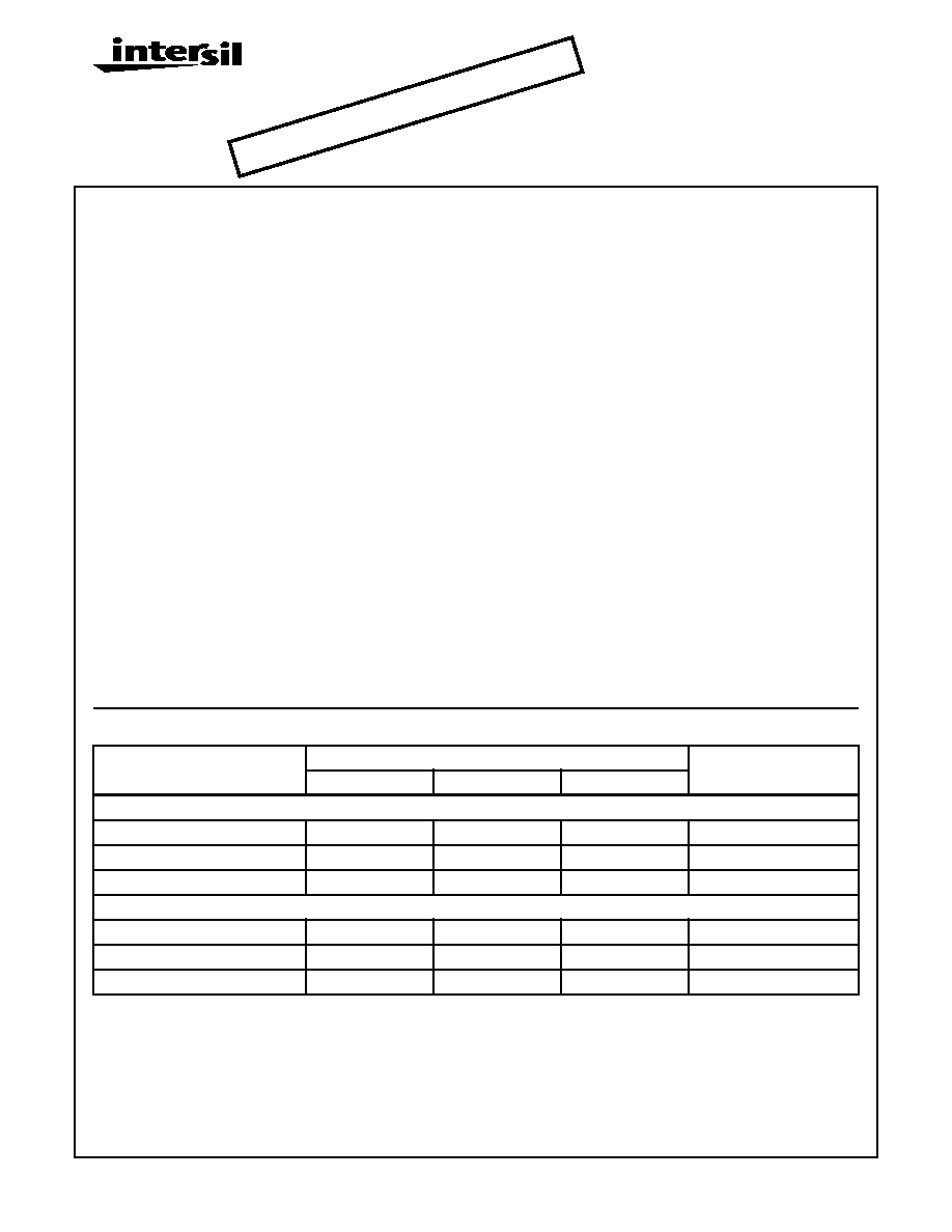
Ordering Information
NON-LINEARITY AT 25
o
C
TEMPERATURE RANGE (
o
C)
PACKAGE
0 to 70
-25 to 85
-55 to 125
BIPOLAR VERSIONS
0.01% (12-bit)
ICL7134BJCJI
ICL7134BJIJI
ICL7134BJMJI
28 Ld CERDIP
0.006% (13-bit)
ICL7134BKCJI
ICL7134BKIJI
ICL7134BKMJI
28 Ld CERDIP
0.003% (14-bit)
ICL7134BLCJI
ICL7134BLIJI
ICL7134BLMJI
28 Ld CERDIP
UNIPLAR VERSIONS
0.01% (12-bit)
ICL7134UJCJI
ICL7134UJIJI
ICL7134UJMJI
28 Ld CERDIP
0.006% (13-bit)
ICL7134UKCJI
ICL7134UKIJI
ICL7134UKMJI
28 Ld CERDIP
0.003% (14-bit)
ICL7134ULCJI
ICL7134ULIJI
ICL7134ULMJI
28 Ld CERDIP
CAUTION: These devices are sensitive to electrostatic discharge; follow proper IC Handling Procedures.
1-888-INTERSIL or 321-724-7143
|
Intersil (and design) is a registered trademark of Intersil Americas Inc.
Copyright © Intersil Americas Inc. 2002. All Rights Reserved
File Number
3113.1
NOT
REC
OMM
END
ED F
OR N
EW D
ESIG
NS
2
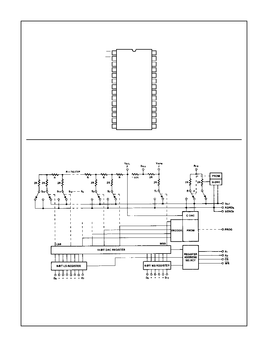
Pinout
ICL7134
(OUTLINE DWG JI)
TOP VIEW
Functional Block Diagram
28
27
26
25
24
23
22
21
20
19
18
17
16
15
CS
WR
(LSB) D
0
D
1
D
2
D
3
D
4
D
5
D
6
D
7
D
8
D
9
D
10
D
11
1
2
3
4
5
6
7
8
9
10
11
12
13
14
A
0
V+
I
OUT
AGND
S
AGND
F
R
FB
R
INV
V
RFL
PROG
D
13
(MSB)
D
12
A
1
DGND
V
RFM
ICL7134

3
Pin Descriptions
28 LEAD
CERDIP
PIN
NAME
PIN DESCRIPTION
1
CS
Chip Select (active low). Enables register write.
2
WR
WRITE, (active low). Writes in register. Equivalent to CS.
3
D
0
Bit 0
Least Significant
4
D
1
Bit1
Input Data Bits (High = True)
5
D
2
Bit 2
6
D
3
Bit 3
7
D
4
Bit 4
8
D
5
Bit 5
9
D
6
Bit 6
10
D
7
Bit 7
11
D
8
Bit 8
12
D
9
Bit 9
13
D
10
Bit 10
14
D
11
Bit 11
15
D
12
Bit 12
16
D
13
Bit 13
Most significant
17
PROG
Used for programming only. Tie to +5V for normal operation.
18
V
RFL
V
REF
for lower bits.
19
R
INV
Summing node for reference inverting amplifier.
20
V
RFM
FV
REF
for MSB only (bipolar)
21
R
FB
Feedback resistor for voltage output applications.
22
DGND
Digital Ground Return.
23
AGND
F
Analog Ground force lines. Use to carry current from internal Analog GND connections. Tied internally to AGND
S
.
24
AGND
S
Analog Ground sense line. Reference point for external circuitry. Pin should carry minimal current; tied internally to
AGND
F
.
25
I
OUT
Current output pin.
26
V+
Positive Supply.
27
A
1
Address 1
Registers Select Lines
28
A
0
Address 0
ICL7134
4
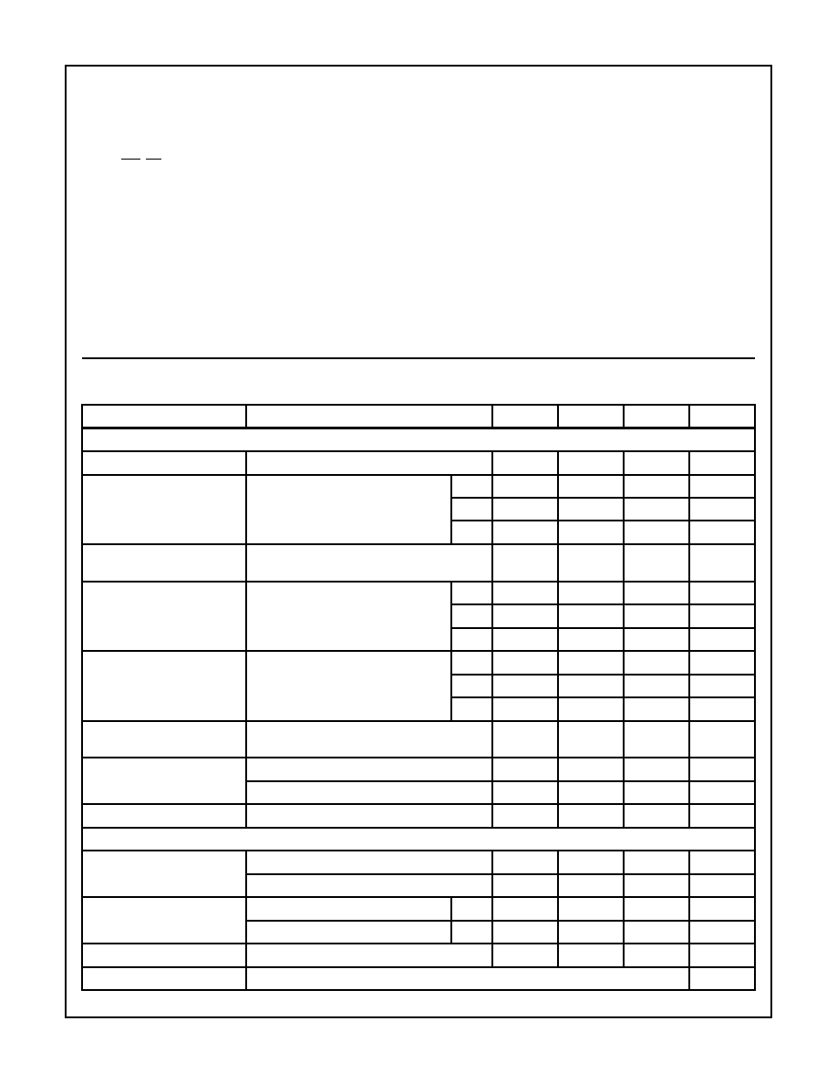
Absolute Maximum Ratings
(Note 1)
Thermal Information
Supply Voltage (V+ to DGND) . . . . . . . . . . . . . . . . . . . -0.3V to 7.5V
V
RFL
, V
RFM
, R
INV
, R
FB
to DGND
. . . . . . . . . . . . . . . . . . . . . . . . ±15V
I
OUT
, AGND
F
, AGND
S
. . . . . . . . . . . . . . . . . . . . . . . . . -0.1V to V+
Current in AGND
S
, AGND
F
. . . . . . . . . . . . . . . . . . . . . . . . . . . 25mA
An, Dn, WR, CS, PROG. . . . . . . . . . . . . . . . . . . . -0.3V to V+ +0.3V
Operating Conditions
Temperature Range
ICL7134XXC . . . . . . . . . . . . . . . . . . . . . . . . . . . . . . . .0
o
C to 70
o
C
ICL7134XXI. . . . . . . . . . . . . . . . . . . . . . . . . . . . . . . -25
o
C to 85
o
C
ICL7134XXM. . . . . . . . . . . . . . . . . . . . . . . . . . . . . -55
o
C to 125
o
C
Storage Temperature Range . . . . . . . . . . . . . . . . . .-65
o
C to 150
o
C
Power Dissipation (Note 2) . . . . . . . . . . . . . . . . . . . . . . . . . . 500mW
Derate Linearly Above 70
o
C @10mW/
o
C
Lead Temperature (Soldering, 10s) . . . . . . . . . . . . . . . . . . . . 300
o
C
CAUTION: Stresses above those listed in "Absolute Maximum Ratings" may cause permanent damage to the device. This is a stress only rating and operation
of the device at these or any other conditions above those indicated in the operational sections of this specification is not implied.
NOTES:
1. All voltages with respect to DGND.
2. Assumes all leads soldered or welded to printed circuit board.
Electrical Specification
V+ = +5V, V
REF
= +10V, T
A
= 25
o
C, AGND = DGND, I
OUT
at Ground Potential,
Unless Otherwise Specified.
PARAMETER
TEST CONDITIONS
MIN
TYP
MAX
UNITS
DC ACCURACY
Resolution
14
-
-
Bits
Non-Linearity
(Notes 3 and 4) Figure 2
J
-
-
±0.012
%FSR
K
-
-
±0.006
%FSR
L
-
-
±0.003
%FSR
Non-Linearity Temperature
Coefficient
Operating Temperature Range (Note 5)
-
±1
±2
ppm/
o
C
Monotonicity
(Note 5)
J
12
-
-
Bits
K
13
-
-
Bits
L
14
-
-
Bits
Gain Error
(Notes 3 and 4)
Figure 1
J
-
-
±0.024
%FSR
K
-
-
±0.012
%FSR
L
-
-
±0.006
%FSR
Gain Error Temperature
Coefficient
(Note 5)
-
±2
±8
ppm/
o
C
Output Leakage Current
(I
OUT
Terminal)
T
A
= 25
o
C
-
-
±10
nA
Operating Temperature Range
-
±60
-
nA
Long Term Stability of I
OUT
1000 Hours, 125
o
C, (Note 5)
-
±10
-
ppm/month
AC ACCURACY
Power Supply Rejection
V+ = ±10%, Figure 2, T
A
= 25
o
C
-
±10
±100
ppm/V
Operating Temperature Range
-
-
±150
ppm/V
Feedthrough Error
V
REF
= 20V
P-P
, 2kHz
U
-
250
-
µV
P-P
Sinewave, Figure 3
B
-
500
-
µV
P-P
Output Current Setting Time
To 1/2 LSB, Figure 4
-
1
-
µs
Output Noise
Equivalent to Johnson Noise of 7k
Resistor, Typical
ICL7134
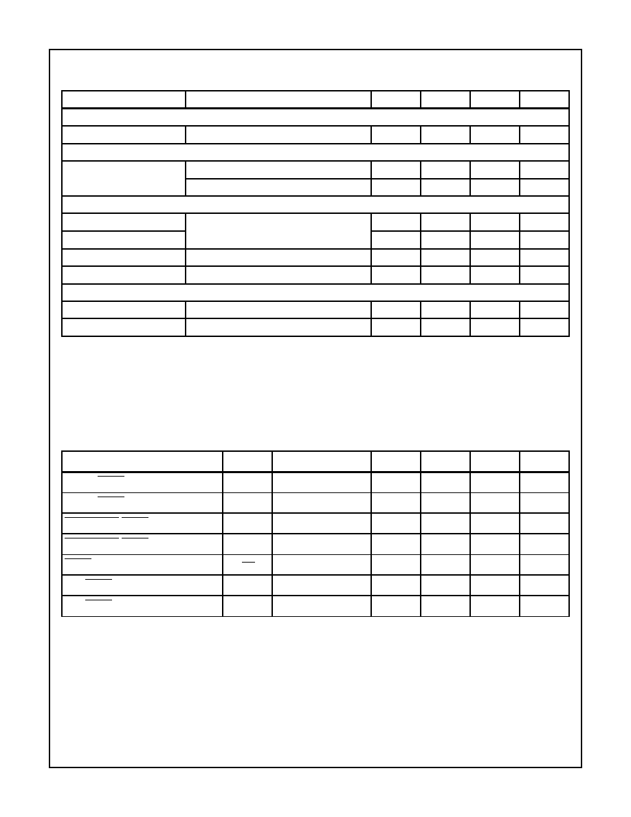
5
REFERENCE INPUT
Input Resistance
V
RFL
= V
RFM
, I
OUT
at Ground
4
7
10
k
ANALOG OUTPUT
Output Capacitance
(I
OUT
Terminal)
DAC Register Outputs All LOW
-
160
-
pF
DAC Register Outputs All HIGH
-
235
-
pF
DIGITAL INPUTS
Low State Threshold
Operating Temperature Range
-
-
0.8
V
High State Threshold
2.4
-
-
V
Input Current
Inputs between DGND to V+
-
-
±1
µA
Input Capacitance
(Note 5)
-
15
-
pF
POWER SUPPLY
Supply Voltage Range
Functional Operation, (Note 6)
3.5
-
6.0
V
Supply Current
Excluding Ladder Network (Note 7)
-
1.0
2.5
mA
NOTES:
3. Full-Scale Range (FSR) is 10V for unipolar mode, 20V (
±10V) for bipolar mode.
4. Using internal feedback and reference inverting resistors.
5. Guaranteed by design, not production tested.
6. Gain error tested to 0.040% FSR, Specifications are not guaranteed.
7. D0 - D13 connected to 2.4V.
Switching Specifications
V+ = 5V, T
A
= 25
o
C, See Timing Diagram
PARAMETER
SYMBOL
TEST CONDITIONS
MIN
TYP
MAX
UNITS
Address-WRITE Set-Up Time
t
AWs
150
-
-
ns
Address-WRITE Hold Time
t
AWh
Note 5
0
-
-
ns
CHIP SELECT-WRITE Set-Up Time
t
CWs
Note 5
0
-
-
ns
CHIP SELECT-WRITE Hold Time
t
CWh
Note 5
0
-
-
ns
WRITE Pulse Width Low
t
WR
200
-
-
ns
Data-WRITE Set-Up Time
t
DWs
200
-
-
ns
Data-WRITE Hold Time
t
DWh
Note 5
0
-
-
ns
Electrical Specification
V+ = +5V, V
REF
= +10V, T
A
= 25
o
C, AGND = DGND, I
OUT
at Ground Potential,
Unless Otherwise Specified. (Continued)
PARAMETER
TEST CONDITIONS
MIN
TYP
MAX
UNITS
ICL7134
6
Test Circuits
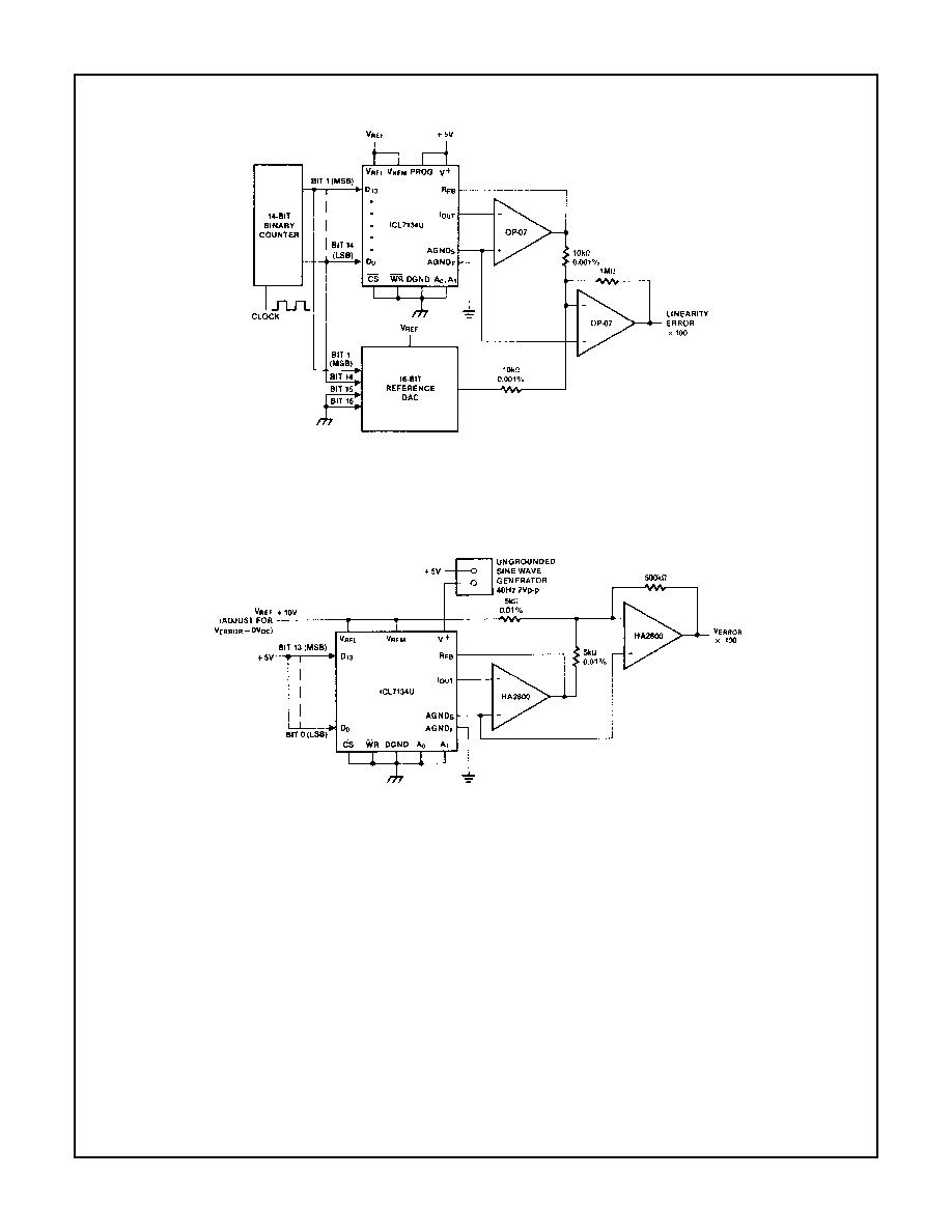
FIGURE 1. NON-LINEARITY TEST CIRCUIT
FIGURE 2. POWER SUPPLY REJECTION TEST CIRCUIT
ICL7134

7
FIGURE 3. FEEDTHROUGH ERROR TEST CIRCUIT
FIGURE 4. OUTPUT CURRENT SETTLING TIME TEST CIRCUIT
Timing Diagrams
FIGURE 5A. USING 14-BIT TRANSPARENT ADDRESSING
Test Circuits
(Continued)
ICL7134

8
FIGURE 5B. USING FULL BUFFER 8-BIT ADDRESSING CAPABILITY
Timing Diagrams
ICL7134
9
Definition of Terms
Nonlinearity - Error contributed by deviation of the DAC
transfer function from a straight line through the end points of
the actual plot of transfer function. Normally expressed as a
percentage of full scale range or in (sub)multiples of 1 LSB.
Resolution - It is addressing the smallest distinct analog out-
put change that a D/A converter can produce. It is commonly
expressed as the number of converter bits. A converter with
resolution of n bits can resolve output changes of 2
-n
of the
full-scale range, e.g. 2
-n
V
REF
for a unipolar conversion. Res-
olution by no means implies linearity.
Settling Time - Time required for the output of a DAC to
settle to within specified error band around its final value
(e.g. 1/2 LSB) for a given digital input change, i.e. all digital
inputs LOW to HIGH and HIGH to LOW.
Gain Error - The difference between actual and ideal analog
output values at full-scale range, i.e., all digital inputs at
HIGH state. It is expressed as a percentage of full-scale
range or in (sub)multiples of 1 LSB.
Feedthrough Error - Error caused by capacitive coupling
from V
REF
to I
OUT
with all digital inputs LOW.
Output Capacitance - Capacitance from I
OUT
terminal to
ground.
Output Leakage Current - Current which appears on I
OUT
terminal when all DAC register outputs are LOW.
Detailed Description
The ICL7134 consists of 14-bit primary DAC, two PROM
controlled correction DACs, input buffer registers, and
microprocessor interface logic (See Functional Block
Diagram). The 14-bit primary DAC is an R-2R thin film
resistor ladder with N-channel MOS SPDT current steering
switches. Precise balancing of the switch resistances, and
all other resistances in the ladder, results in excellent
temperature stability.
True 14-bit linearity is achieved by programming a floating poly-
silicon gate PROM array which controls two correction DAC cir-
cuits. A 6-bit gain correction DAC, or G-DAC, diverts up to 2%
of the feedback resistor's current to Analog GND and reduces
the gain error to less than 1 LSB, or 0.006%. The 5 most
significant outputs of the DAC register address a 31-word
PROM array that controls a 12-bit linearity correction DAC, or
C-DAC. For every combination of the primary DAC's 5 most
significant bits, a different C-DAC code is selected. This allows
correction of superposition errors, caused by bit interaction on
the primary resistor ladder's current output bus and by voltage
non-linearity in the feedback resistor. Superposition errors can-
not be corrected by any method which corrects individual bits
only, such as laser trimming. Since the PROM programming
occurs in packaged form, it corrects for resistor shifts caused by
the thermal stresses of packaging. These packaging shifts limit
the accuracy that can be achieved using wafer level correction
methods such as laser trimming, which has also been found to
degrade the time stability of thin film resistors at the 14-bit level.
Analog Section
The ICL7134 inherently provides both unipolar and bipolar
operation. The bipolar application circuit (Figure 6) requires
one additional op-amp but no external resistors. The two on-
chip resistors, R
INV1
and R
INV2
, together with the op-amp,
form a voltage inverter which drives the MSG reference ter-
minal, V
RFM
, to -V
REF
, where V
REF
is the voltage applied at
the less significant bits' reference terminal, V
RFL
. Notice the
values of 1.95R and 2R for the R
INV1
and R
INV2
. The V
RFM
absolute value is about 2.5% higher than the V
RFL
. This is
necessary so that the gain error can be corrected. This
reverses the weight of the MSG, and gives the DAC a 2's
complement transfer function. The op-amp and reference
connection to V
RFM
and V
RFL
can be reversed, without
affecting linearity, but a small gain error will be introduced.
For unipolar operation the V
RFM
and V
RFL
terminals are
both tied to V
REF
, and the R
INV
pin is left unconnected.
Since the PROM correction codes required are different for
bipolar and unipolar operation, the ICL7134 is available in
two different versions; the ICL7134U, which is corrected for
unipolar operation, and the ICL7134B, which is programmed
for bipolar application. The feedback resistance is also differ-
ent in the two versions, and is switched under PROM control
from `R' in the unipolar device to `2R' in the bipolar part.
These feedback resistors have a dummy (always ON) switch
in series to compensate for the effect of the ladder switches.
This greatly improves the gain temperature coefficient and
the power supply rejection of the device.
FIGURE 6. BIPOLAR OPERATION WITH INVERTED V
REF
TO MSB
ICL7134
10
Digital Section
Two levels of input buffer registers allow loading of data from
an 8-bit or 16-bit data bus. The A
0
and A
1
, pins select one of
four operations: 1) load the LS-buffer register with the data
at inputs D
0
to D
7
; 2) load the MS-buffer register with the
data at inputs D
8
to D
13
; 3) load the DAC register with the
contents of the MS and LS-buffer registers and 4) load the
DAC register directly from the data input pins (See Table 1).
The CS and WR pins must be low to allow data transfers to
occur. When direct loading is selected (CS, WR, A
0
and A
1
low) the registers are transparent, and the data input pins
control the DAC output directly. The other modes of opera-
tion allow double buffered loading of the DAC from an 8-bit
bus.
These input data pins are also used to program the PROM
under control of the PROG pin. This is done in manufactur-
ing, and for normal operation the PROG pin should be tied to
V+ (+5V).
Applications
GENERAL RECOMMENDATIONS
Grounding
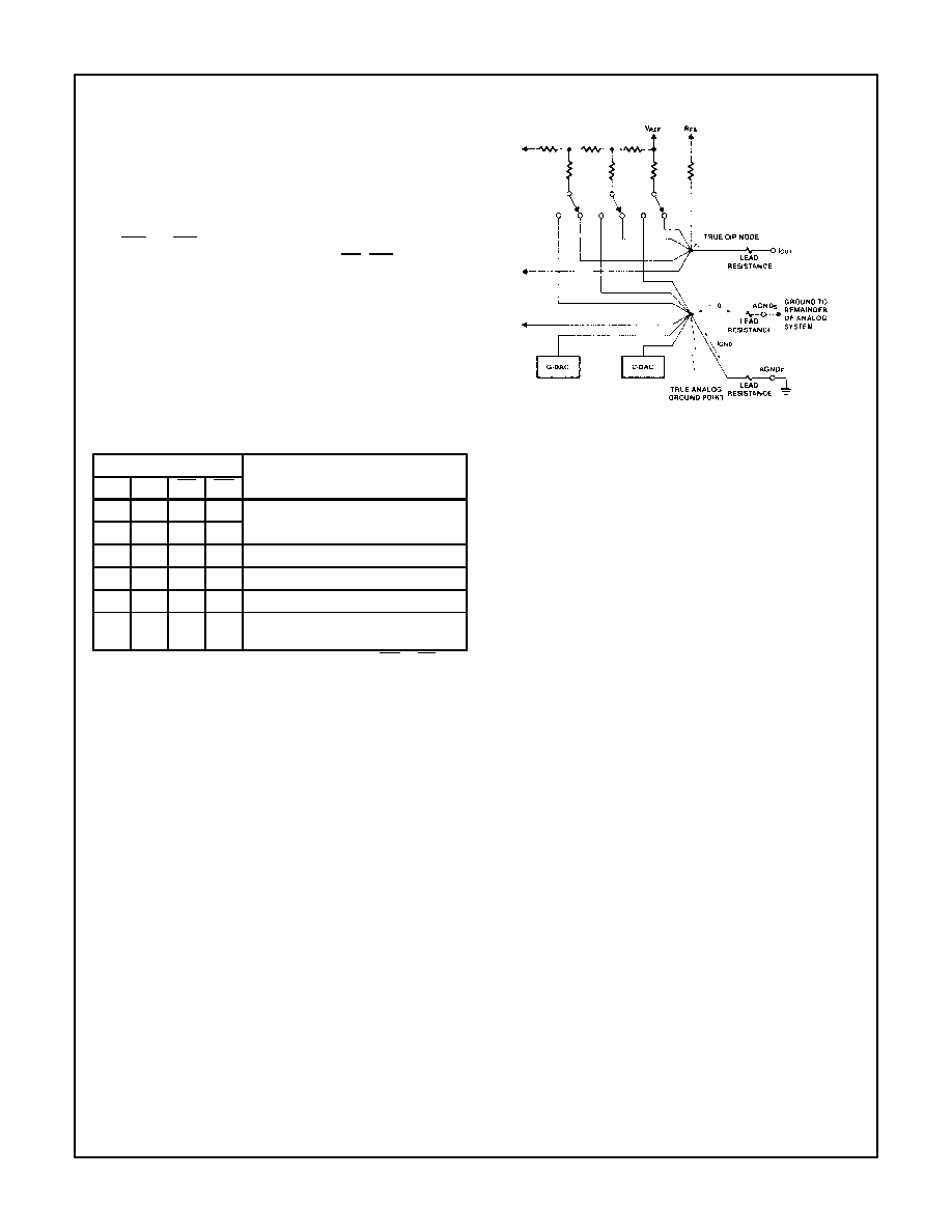
Careful consideration must be given to grounding in any
14-bit accuracy system. The current into the analog ground
point inside the chip varies significantly with the input code
value, and the inevitable resistances between this point and
any external connection pint can lead to significant voltage
drop errors. For this reason, two separate leads are brought
out from this point on the IC, the AGND
F
and AGND
S
pins.
The varying current should be absorbed through the AGND
F
pin, and the AGND
S
pin will then accurately reflect the
voltage on the internal current summing point, as shown in
Figure 7. Thus output signals should be referenced to the
sense pin AGND
S
, as shown in the various application
circuits.
Operational Amplifier Selection
To maintain static accuracy, the I
OUT
potential must be
exactly equal to the AGND
S
potential. Thus output amplifier
selection is critical, in particular low input bias current (less
than 2nA), low offset voltage (less than 25
µV) are advisable
if the highest accuracy is needed. Maintaining a low input
offset over a 0V to 10V range also requires that the output
amplifier has a high open loop gain (A
VOL
> 400k for
effective input offset less than 25
µV).
The reference inverting amplifier used in the bipolar mode
circuit must also be selected carefully. If 14-bit accuracy is
desired without adjustment, low input bias current (less than
1nA), low offset voltage (less than 50
µV), and high gain
(greater than 400k) are recommended. If a fixed reference
voltage is used, the gain requirement can be relaxed. For
highest accuracy (better than 13-bits), and additional
op-amp may be needed to correct for IR drop on the Analog
GROUND line (op-amp A
2
in Figure 9). This op-amp should
be selected for low bias current (less than 2nA) and low
offset voltage (less than 50
µV).
The op-amp requirements can be readily met by use of an
ICL7650 chopper stabilized device. For faster setting time,
an HA26XX can be used with an ICL7650 providing
automatic offset null (see A053 applications note for details)
The output amplifier's non-inverting input should be tied
directly to AGND
S
. A bias current compensation resistor is of
limited use since the output impedance at the summing node
depends on the code being converted in an unpredictable
way. If gain adjustment is required, low tempco (approxi-
mately 50ppm/
o
C) resistors or trim-pots should be selected.
Power Supplies
The V+ (pin 25) power supply should have a low noise level,
and no transients exceeding 7 volts. Note that the absolute
maximum for digital input voltage is V+ +0.3V, therefore V+
must be applied before digital inputs are allowed to go high.
Unused digital inputs must be connected to GND or V+ for
proper operation.
Unipolar Binary Operation (ICL7134U)
The circuit configuration for unipolar mode operation
(ICL7134U) is shown in Figure 8. With positive and negative
V
REF
values the circuit is capable of two-quadrant
multiplication. The "digital input code/analog output value"
table for unipolar mode is given in Table 2. The Schottky
diode (HP5082-2811 or equivalent) protects I
OUT
from
TABLE 1. DATA LOADING CONTROLS
CONTROL I/P
ICL7134 OPERATION
A
0
A
1
CS
WR
X
X
X
1
No Operation, Device Not Selected.
X
X
1
X
0
0
0
0
Load All Registers from Data Bus.
0
1
0
0
Load LS Register from Data Bus.
1
0
0
0
Load MS Register from Data Bus.
1
1
0
0
Load DAC Register from MS and LS
Register.
NOTE: Data is latched on LO-HI transition of either WR or CS.
FIGURE 7. GROUND CONNECTIONS
ICL7134

11
negative excursions which could damage the device, and is
only necessary with certain high spped amplifiers. For
applications where the output reference ground point is
established somewhere other than at the DAC, the circuit of
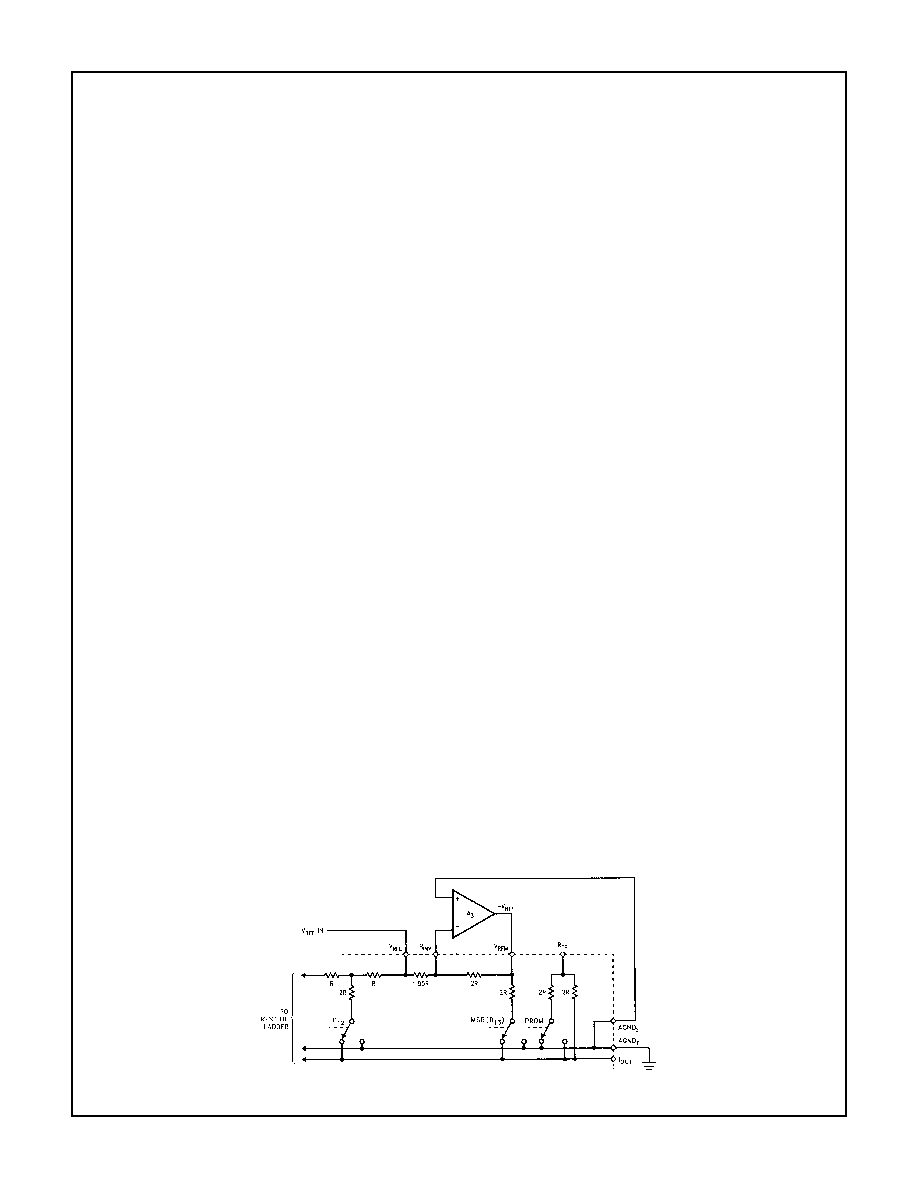
Figure 9 can be used. Here, op-amp A
2
removes the slight
error due to IR voltage drop between the internal Analog
GrouND node and the external ground connection. For
13-bit or lower accuracy, omit A
2
and connect AGND
F
and
AGND
S
directly to ground through as low a resistance as
possible.
Zero Offset Adjustment
1. Connect all data inputs and WR, CS, A
0
and A
1
to
DGND.
2. Adjust offset zero-adjust trim-pot of the operational ampli-
fier A
2
, if used, for a maximum of 0V
±50µV at AGND
S
.
3. Adjust the offset zero-adjust trim-pot of the output
op-amp, A
1
, for a maximum of 0V
±50µV at V
OUT
.
Gain Adjustment (Optional)
1. Connect all data inputs to V+, connect WR, CS, A
0
and A
1
to DGND.
2. Monitor V
OUT
for a -V
REF
(1 - 1/2
14
) reading.
3. To decrease V
OUT
, connect a series resistor of 5
or less
between the reference voltage and the V
RFM
and V
RFL
terminals (pins 20 and 18).
4. To increase V
OUT
, connect a series resistor of 5
or less
between A
1
output and the R
FB
terminal (pin 21).
Bipolar (2's Complement) Operation (ICL7134B)
The circuit configuration for bipolar mode operation
(ICL7134B) is shown in Figure 10. Using 2's complement
digital input codes and positive and negative reference
voltage values, four-quadrant multiplication is obtained. The
"digital input code/analog output value" table for bipolar
mode is given in Table 3. Amplifier A
3
, together with internal
resistors R
INV1
and R
INV2
, forms a simple voltage inverter
circuit. The MSB ladder leg sees a reference input of
approximately -V
REF
, so the MSB's weight is reversed from
the polarity of the other bits. In addition, the ICL7134B's
feedback resistance is switched to 2R under PROM control,
so that the bipolar output range is +V
REF
to -V
REF
(1 -
1/2
13
). Again, the grounding arrangement of Figure 9 can be
used if necessary.
FIGURE 8. UNIPOLAR BINARY, TWO-QUADRANT
MULTIPLYING CIRCUIT
FIGURE 9. UNIPOLAR BINARY OPERATION WITH FORCED
GROUND
TABLE 2. CODE TABLE - UNIPOLAR BINARY OPERATION
DIGITAL INPUT
ANALOG OUTPUT
1 1 1 1 1 1 1 1 1 1 1 1 1 1
-V
REF
(1 - 1/2
14
)
1 0 0 0 0 0 0 0 0 0 0 0 0 1
-V
REF
(1/2 + 1/2
14
)
1 0 0 0 0 0 0 0 0 0 0 0 0 0
-V
REF
/2
0 1 1 1 1 1 1 1 1 1 1 1 1 1
-V
REF
(1/2 - 1/2
14
)
0 0 0 0 0 0 0 0 0 0 0 0 0 1
-V
REF
(1/2
14
)
0 0 0 0 0 0 0 0 0 0 0 0 0 0
0
TABLE 3. CODE TABLE - BIPOLAR (2'S COMPLEMENT)
OPERATION
DIGITIAL INPUT
ANALOG OUTPUT
0 1 1 1 1 1 1 1 1 1 1 1 1 1
-V
REF
(1 - 1/2
13
)
0 0 0 0 0 0 0 0 0 0 0 0 0 1
-V
REF
(1/2
13
)
0 0 0 0 0 0 0 0 0 0 0 0 0 0
0
1 1 1 1 1 1 1 1 1 1 1 1 1 1
V
REF
(1/2
13
)
1 0 0 0 0 0 0 0 0 0 0 0 0 1
V
REF
(1 - 1/2
13
)
1 0 0 0 0 0 0 0 0 0 0 0 0 0
V
REF
ICL7134

12
Offset Adjustment
1. Connect all data inputs and WR, CS, A
0
and A
1
to
DGND.
2. Adjust the offset zero-adjust trim-pot of the operational
amplifier A
2
, if used, for a maximum of 0V
±50µV at
AGND
S
.
3. Set data to 000000....00. Adjust the offset zero-adjust
trim-pot of any output op-amp A
1
, for a maximum of 0V
±50µV at V
OUT
.
4. Connect D
13
(MSB) data input to V+.
5. Adjust the offset zero-adjust trim-pot of op-amp A
3
for a
maximum of 0V
±50µV at the R
INV
terminal (pin 19).
Gain Adjustment (Optional)
1. Connect WR, CS, A
0
and A
1
to DGND.
2. Connect D
0
, D
1
... D
12
to V+, D
13
(MSB) to DGND.
3. Monitor V
OUT
for a -V
REF
(1 - 1/2
13
) reading.
4. To increase V
OUT
, connect a series resistor of 10
or
less between the A
1
output and the R
FB
terminal (pin 21).
5 To decrease V
OUT
, connect a series resistor of 5
or
less between the reference voltage and the V
RFL
termi-
nal (pin 18).
Processor Interfacing
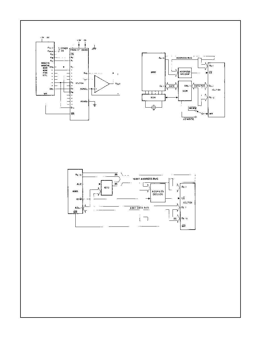
The ease of interfacing to a processor can be seen from
Figure 11, which shows the ICL7134 connected to an 8035
or any other processor such as an 8049. The data bus feeds
into both register inputs; three port lines, in combination with
the WR line, control the byte-wide loading into these
registers and then the DAC register. A complete DAC set-up
requies 4 write instructions to the port, to set up the address
and CS lines, and 3 external data transfers, one a dummy
for the final transfer to the DAC register.
A similar arrangement can be used with an 8080A, 8228,
and 8224 chip set. Figure 12 shows the circuit, which can be
arranged as a memory-mapped interface (using MEMW) or
as an I/O-mapped interface (using I/O WRITE). See A020
and R005 for discussions of the relative merits of memory-
mapped versus I/O-mapped interfacing, as well as some
other ideas on interfacing with 8080 processors. The 8085
processor has a very similar interface, except that the con-
trol lines available are slightly different, as shown in Figure
13. The decoding of the IO/M line, which controls memory-
mapped or I/O-mapped operation, is arbitrary, and can be
omitted if not necessary. Neither the MC680X nor R650X
processor families offer specific I/O operations. Figure 14
shows a suitable interface to either of these systems, using a
direct connection. Several other decoding options can be
used, depending on the other control signals generated in
the system. Note that the R650X family does not require
VMA to be decoded with the address lines.
FIGURE 10. BIPOLAR (2'S COMPLEMENT), FOUR-QUADRANT MULTIPLYING CIRCUIT
ICL7134
13
FIGURE 11. ICL7134 INTERFACE TO 8048 SYSTEM
FIGURE 12. INTERFACE TO 8080 SYSTEM
FIGURE 13. 8085 SYSTEM INTERFACE
ICL7134

14
Digital Feedthrough
All of the direct interfaces shown above can suffer from a
capacitive coupling problem. The 14 data pins, and 4 control
pins, all tied to active lines on a microprocessor bus, and in
close proximity to the sensitive DAC circuitry, can couple
pseudo-random spikes into the analog output. Careful board
layout and shielding can minimize the problems (see PC
layout), and clearly wire-wrap type sockets should never be
used. Nevertheless, the inherent capacitance of the package
alone can lead to unacceptable digital feedthrough in many
cases. The only solution is to keep the digital input lines as
inactive as possible. One easy way to do this is to use the
peripheral interface circuitry available with all the systems
previously discussed. These generally allow only 8 bits to be
updated at any one time, but a little ingenuity will avoid diffi-
culties with DAC steps that would result from partial updates.
The problem can be solved for the 8048 family by tying the
14 port lines to the data input lines, with CS, A
0
and A
1
held
low, and using only the WR line to enter the data into the
DAC (as shown in Figure 15). WR is well separated from the
analog lines on the ICL7134, and is usually not a very active
line in 8048 systems. Additional "protection" can be achieved
by gating the processor WR line with another port line. The
same type of technique can be employed in the 8080/85
systems by using an 8255 PIA (peripheral Interface adaptor)
(Figure 16) and in the MC680X and R650X systems by using
an MC6820 (R6520) PIA.
Successive Approximation A/D Converters
Figure 17 shows an ICL7134B-based circuit for a bipolar
input high speed A/D converter, using two AM25LO3s to
form a 14-bit successive approximation register. The
comparator is a two-stage circuit with and HA2605 front-end
amplifier, used to reduce setting time problems at the
summing node (see A020). Careful offset-nulling of this
amplifier is needed, and if wide temperature range operation
is desired, and auto-null circuit using an ICL7650 is probably
advisable (see A053). The clock, using two Schmitt trigger
TTL gates, runs at a slower rate for the first 8 bits, where
setting-time is most critical, than for the last 6 bits. The short-
cycle line is shown tied to the 15th bit; if fewer bits are
required, it can be moved up accordingly. The circuit will
free-run if the HOLD/RUN input is held low, but will stop after
completing a conversion if the pin is high at that time. A low-
going pulse will restart it. The STATUS output indicates
when the device is operating, and the falling edge indicates
the availability of new data. A unipolar version may be con-
structed by tying the MSB (D
13
) on an ICL7134U to pin 14
on the first AM25L03, deleting the reference inversion
amplifier A
4
, and tying V
RFM
and V
RFL
.
FIGURE 14. R650X AND MC680X FAMILIES' INTERFACE TO
ICL7134
FIGURE 15. AVOIDING DIGITAL FEEDTHROUGH IN AN 8048
TO ICL7134 INTERFACE
FIGURE 16. ICL7134 TO 8048/80/85 INTERFACE WITH LOW FEEDTHROUGH
ICL7134

15
FIGURE 17. SUCCESSIVE APPROXIMATION A/D CONVERTER
ICL7134
16
PC Board Layout
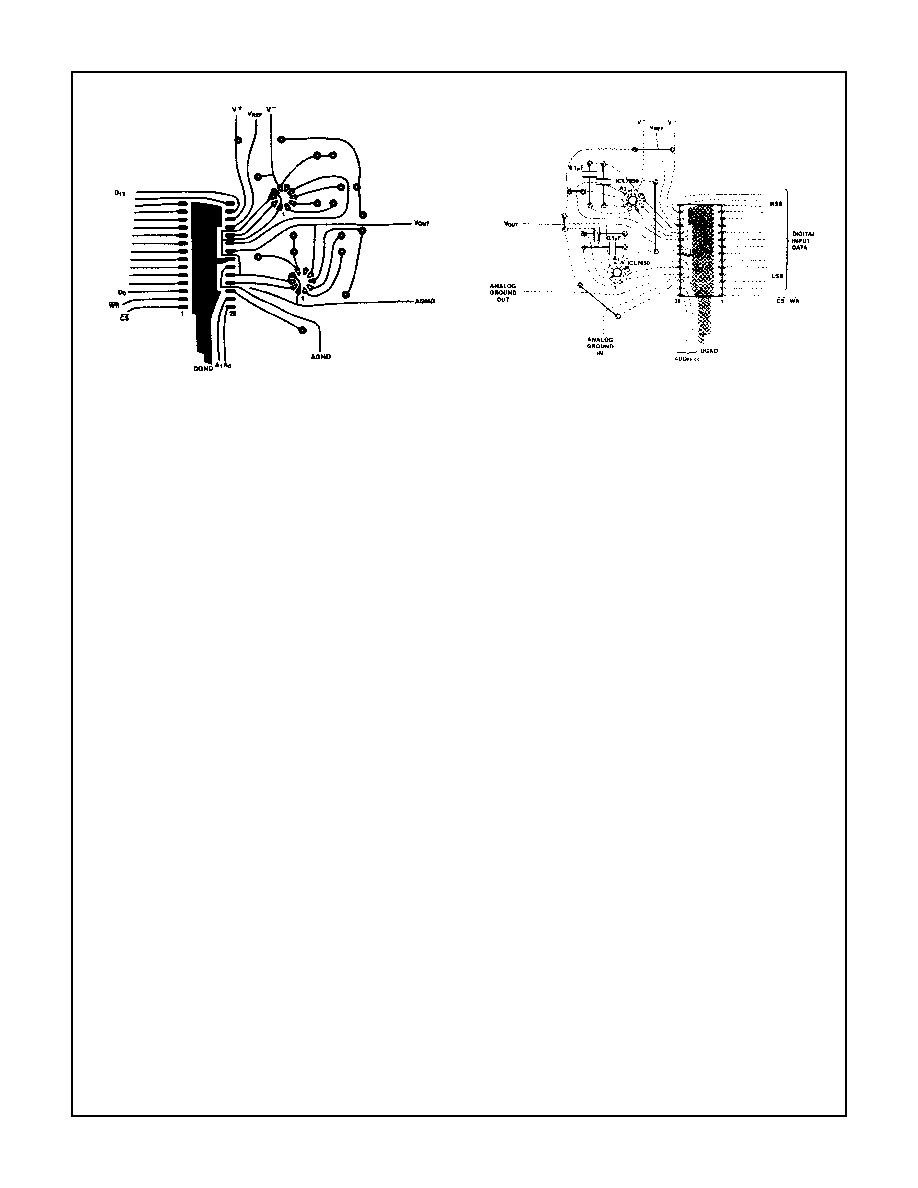
Great care should be taken in the board layout to minimize
ground loop and similar "hidden resistor" problems, as well
as to minimize digital signal feedthrough. A suitable layout
for the immediate vicinity of the ICL7134 is shown in Figure
18, and may be used as a guide.
Application Notes
Some applications bulletins that may be found useful are
listed here:
A002 "Principles of Data Acquisition and Conversion"
A018 "Do's and Don'ts of Applying A/D Converters", by
Peter Bradshaw and Skip Osgood.
A020 "A Cookbook Approach to High Speed Data
Acquisition and Microprocessor Interfacing,", by Ed
Sliger.
A042 "Interpretation of Data Converters Accuracy
Specifications"
R005 "Interfacing Data Converters & Microprocessor", by
Peter Bradshaw et al., Electronics, Dec 9, 1976.
Most of these are avilable in the Intersil Data Acquisition
Handbook, together with other material.
FIGURE 18A. PRONTED CIRCUIT SIDE OF CARD (SINGLE
SIDED BOARD)
FIGURE 18B. TOP SIDE WITH COMPONENT PLACEMENT
FIGURE 18. PRINTED CIRCUIT BOARD LAYOUT (BIPOLAR CIRCUIT, SEE FIGURE 10)