 | –≠–ª–µ–∫—Ç—Ä–æ–Ω–Ω—ã–π –∫–æ–º–ø–æ–Ω–µ–Ω—Ç: ICL7612 | –°–∫–∞—á–∞—Ç—å:  PDF PDF  ZIP ZIP |
1
File Number
2919.5
ICL7611, ICL7612
1.4MHz, Low Power CMOS Operational
Amplifiers
The ICL761X/762X/764X series is a family of monolithic
CMOS operational amplifiers. These devices provide the
designer with high performance operation at low supply
voltages and selectable quiescent currents, and are an ideal
design tool when ultra low input current and low power
dissipation are desired.
The basic amplifier will operate at supply voltages ranging
from
±
1V to
±
8V, and may be operated from a single
Lithium cell.
A unique quiescent current programming pin allows setting
of standby current to 1mA, 100
µ
A, or 10
µ
A, with no external
components. This results in power consumption as low as
20
µ
W. The output swing ranges to within a few millivolts of
the supply voltages.
Of particular significance is the extremely low (1pA) input
current, input noise current of 0.01pA/
Hz, and 10
12
input
impedance. These features optimize performance in very
high source impedance applications.
The inputs are internally protected. Outputs are fully
protected against short circuits to ground or to either supply.
AC performance is excellent, with a slew rate of 1.6V/
µ
s, and
unity gain bandwidth of 1MHz at I
Q
= 1mA.
Because of the low power dissipation, junction temperature
rise and drift are quite low. Applications utilizing these
features may include stable instruments, extended life
designs, or high density packages.
Features
∑ Wide Operating Voltage Range . . . . . . . . . . .
±
1V to
±
8V
∑ High Input Impedance . . . . . . . . . . . . . . . . . . . . . . 10
12
∑ Programmable Power Consumption . . . . . . Low as 20
µ
W
∑ Input Current Lower Than BIFETs . . . . . . . . . . . 1pA (Typ)
∑ Output Voltage Swing . . . . . . . . . . . . . . . . . . . V+ and V-
∑ Input Common Mode Voltage Range Greater Than Supply
Rails (ICL7612)
Applications
∑ Portable Instruments
∑ Telephone Headsets
∑ Hearing Aid/Microphone Amplifiers
∑ Meter Amplifiers
∑ Medical Instruments
∑ High Impedance Buffers
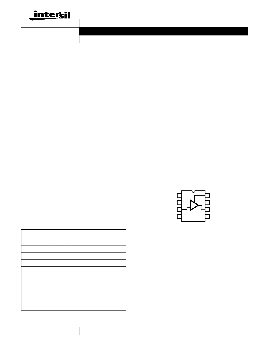
Pinouts
ICL7611, ICL7612
(PDIP, SOIC)
TOP VIEW
Ordering Information
PART
NUMBER
TEMP.
RANGE
(
o
C)
PACKAGE
PKG.
NO.
ICL7611BCPA
0 to 70
8 Ld PDIP - B Grade
E8.3
ICL7611DCPA
0 to 70
8 Ld PDIP - D Grade
E8.3
ICL7611DCBA
0 to 70
8 Ld SOIC - D Grade
M8.15
ICL7611DCBA-T
0 to 70
8 Ld SOIC - D Grade
Tape and Reel
M8.15
ICL7612BCPA
0 to 70
8 Ld PDIP - B Grade
E8.3
ICL7612DCPA
0 to 70
8 Ld PDIP - D Grade
E8.3
ICL7612DCBA
0 to 70
8 Ld SOIC - D Grade
M8.15
ICL7612DCBA-T
0 to 70
8 Ld SOIC - D Grade
Tape and Reel
M8.15
BAL
-IN
+IN
V-
1
2
3
4
8
7
6
5
I
Q
SET
V+
OUT
BAL
+
-
Data Sheet
October 1999
CAUTION: These devices are sensitive to electrostatic discharge; follow proper IC Handling Procedures.
1-888-INTERSIL or 321-724-7143
|
Copyright
©
Intersil Corporation 1999
2
Absolute Maximum Ratings
Thermal Information
Supply Voltage V+ to V- . . . . . . . . . . . . . . . . . . . . . . . . . . . . . . . 18V
Input Voltage . . . . . . . . . . . . . . . . . . . . . . . . . . . V- -0.3 to V+ +0.3V
Differential Input Voltage (Note 1) . . . . . . . . . [(V+ +0.3) - (V- -0.3)]V
Duration of Output Short Circuit (Note 2). . . . . . . . . . . . . . Unlimited
Operating Conditions
Temperature Range
ICL76XXC . . . . . . . . . . . . . . . . . . . . . . . . . . . . . . . . 0
o
C to 70
o
C
Thermal Resistance (Typical, Note 3)
JA
(
o
C/W)
PDIP Package . . . . . . . . . . . . . . . . . . . . . . . . . . . . .
130
SOIC Package . . . . . . . . . . . . . . . . . . . . . . . . . . . . .
170
Maximum Junction Temperature (Plastic Package) . . . . . . . .150
o
C
Maximum Storage Temperature Range . . . . . . . . . . -65
o
C to 150
o
C
Maximum Lead Temperature (Soldering 10s) . . . . . . . . . . . . 300
o
C
(SOIC - Lead Tips Only)
CAUTION: Stresses above those listed in "Absolute Maximum Ratings" may cause permanent damage to the device. This is a stress only rating and operation of the
device at these or any other conditions above those indicated in the operational sections of this specification is not implied.
NOTES:
1. Long term offset voltage stability will be degraded if large input differential voltages are applied for long periods of time.
2. The outputs may be shorted to ground or to either supply, for V
SUPPLY
10V. Care must be taken to insure that the dissipation rating is not
exceeded.
3.
JA
is measured with the component mounted on an evaluation PC board in free air.
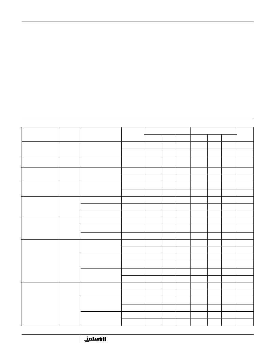
Electrical Specifications
V
SUPPLY
=
±
5V, Unless Otherwise Specified
PARAMETER
SYMBOL
TEST
CONDITIONS
TEMP (
o
C)
ICL7611B, ICL7612B
ICL7611D, ICL7612D
UNITS
MIN
TYP
MAX
MIN
TYP
MAX
Input Offset Voltage
V
OS
R
S
100k
25
-
-
5
-
-
15
mV
Full
-
-
7
-
-
20
mV
Temperature
Coefficient of V
OS
V
OS
/
T
R
S
100k
-
-
15
-
-
25
-
µ
V/
o
C
Input Offset Current
I
OS
25
-
0.5
30
-
0.5
30
pA
Full
-
-
300
-
-
300
pA
Input Bias Current
I
BIAS
25
-
1.0
50
-
1.0
50
pA
Full
-
-
400
-
-
400
pA
Common Mode
Voltage Range
(Except ICL7612)
V
CMR
I
Q
= 10
µ
A
25
±
4.4
-
-
±
4.4
-
-
V
I
Q
= 100
µ
A
25
±
4.2
-
-
±
4.2
-
-
V
I
Q
= 1mA
25
±
3.7
-
-
±
3.7
-
-
V
Extended Common
Mode Voltage Range
(ICL7612 Only)
V
CMR
I
Q
= 10
µ
A
25
±
5.3
-
-
±
5.3
-
-
V
I
Q
= 100
µ
A
25
+5.3, -5.1
-
-
+5.3, -5.1
-
-
V
I
Q
= 1mA
25
+5.3, -4.5
-
-
+5.3, -4.5
-
-
V
Output Voltage Swing
V
OUT
I
Q
= 10
µ
A, R
L
= 1M
25
±
4.9
-
-
±
4.9
-
-
V
Full
±
4.8
-
-
±
4.8
-
-
V
I
Q
= 100
µ
A, R
L
= 100k
25
±
4.9
-
-
±
4.9
-
-
V
Full
±
4.8
-
-
±
4.8
-
-
V
I
Q
= 1mA, R
L
= 10k
25
±
4.5
-
-
±
4.5
-
-
V
Full
±
4.3
-
-
±
4.3
-
-
V
Large Signal Voltage
Gain
A
VOL
V
O
=
±
4.0V, R
L
= 1M
,
I
Q
= 10
µ
A
25
80
104
-
80
104
-
dB
Full
75
-
-
75
-
-
dB
V
O
=
±
4.0V, R
L
= 100k
,
I
Q
= 100
µ
A
25
80
102
-
80
102
-
dB
Full
75
-
-
75
-
-
dB
V
O
=
±
4.0V, R
L
= 10k
,
I
Q
= 1mA
25
76
83
-
76
83
-
dB
Full
72
-
-
72
-
-
dB
ICL7611, ICL7612
3
Unity Gain Bandwidth
GBW
I
Q
= 10
µ
A
25
-
0.044
-
-
0.044
-
MHz
I
Q
= 100
µ
A
25
-
0.48
-
-
0.48
-
MHz
I
Q
= 1mA
25
-
1.4
-
-
1.4
-
MHz
Input Resistance
R
IN
25
-
10
12
-
-
10
12
-
Common Mode
Rejection Ratio
CMRR
R
S
100k
,
I
Q
= 10
µ
A
25
70
96
-
70
96
-
dB
R
S
100k
,
I
Q
= 100
µ
A
25
70
91
-
70
91
-
dB
R
S
100k
,
I
Q
= 1mA
25
60
87
-
60
87
-
dB
Power Supply
Rejection Ratio
(V
SUPPLY
=
±
8V to
±
2V)
PSRR
R
S
100k
,
I
Q
= 10
µ
A
25
80
94
-
80
94
-
dB
R
S
100k
,
I
Q
= 100
µ
A
25
80
86
-
80
86
-
dB
R
S
100k
,
I
Q
= 1mA
25
70
77
-
70
77
-
dB
Input Referred Noise
Voltage
e
N
R
S
= 100
, f = 1kHz
25
-
100
-
-
100
-
nV/
Hz
Input Referred Noise
Current
i
N
R
S
= 100
, f = 1kHz
25
-
0.01
-
-
0.01
-
pA/
Hz
Supply Current
(No Signal, No Load)
I
SUPPLY
I
Q
SET = +5V, Low Bias
25
-
0.01
0.02
-
0.01
0.02
mA
I
Q
SET = 0V,
Medium Bias
25
-
0.1
0.25
-
0.1
0.25
mA
I
Q
SET = -5V, High Bias
25
-
1.0
2.5
-
1.0
2.5
mA
Channel Separation
V
O1
/V
O2
A
V
= 100
25
-
120
-
-
120
-
dB
Slew Rate
(A
V
= 1, C
L
= 100pF,
V
IN
= 8V
P-P
)
SR
I
Q
= 10
µ
A, R
L
= 1M
25
-
0.016
-
-
0.016
-
V/
µ
s
I
Q
= 100
µ
A, R
L
= 100k
25
-
0.16
-
-
0.16
-
V/
µ
s
I
Q
= 1mA, R
L
= 10k
25
-
1.6
-
-
1.6
-
V/
µ
s
Rise Time
(V
IN
= 50mV,
C
L
= 100pF)
t
r
I
Q
= 10
µ
A, R
L
= 1M
25
-
20
-
-
20
-
µ
s
I
Q
= 100
µ
A, R
L
= 100k
25
-
2
-
-
2
-
µ
s
I
Q
= 1mA, R
L
= 10k
25
-
0.9
-
-
0.9
-
µ
s
Overshoot Factor
(V
IN
= 50mV,
C
L
= 100pF)
OS
I
Q
= 10
µ
A, R
L
= 1M
25
-
5
-
-
5
-
%
I
Q
= 100
µ
A, R
L
= 100k
25
-
10
-
-
10
-
%
I
Q
= 1mA, R
L
= 10k
25
-
40
-
-
40
-
%
Electrical Specifications
V
SUPPLY
=
±
5V, Unless Otherwise Specified (Continued)
PARAMETER
SYMBOL
TEST
CONDITIONS
TEMP (
o
C)
ICL7611B, ICL7612B
ICL7611D, ICL7612D
UNITS
MIN
TYP
MAX
MIN
TYP
MAX
Electrical Specifications
V
SUPPLY
=
±
1V, I
Q
= 10
µ
A, Unless Otherwise Specified
PARAMETER
SYMBOL
TEST
CONDITIONS
TEMP
(
o
C)
ICL7611B, ICL7612B
UNITS
MIN
TYP
MAX
Input Offset Voltage
V
OS
R
S
100k
25
-
-
5
mV
Full
-
-
7
mV
Temperature Coefficient of V
OS
V
OS
/
T
R
S
100k
-
-
15
-
µ
V/
o
C
Input Offset Current
I
OS
25
-
0.5
30
pA
Full
-
-
300
pA
Input Bias Current
I
BIAS
25
-
1.0
50
pA
Full
-
-
500
pA
Common Mode Voltage Range
(Except ICL7612)
V
CMR
25
±
0.6
-
-
V
ICL7611, ICL7612
4
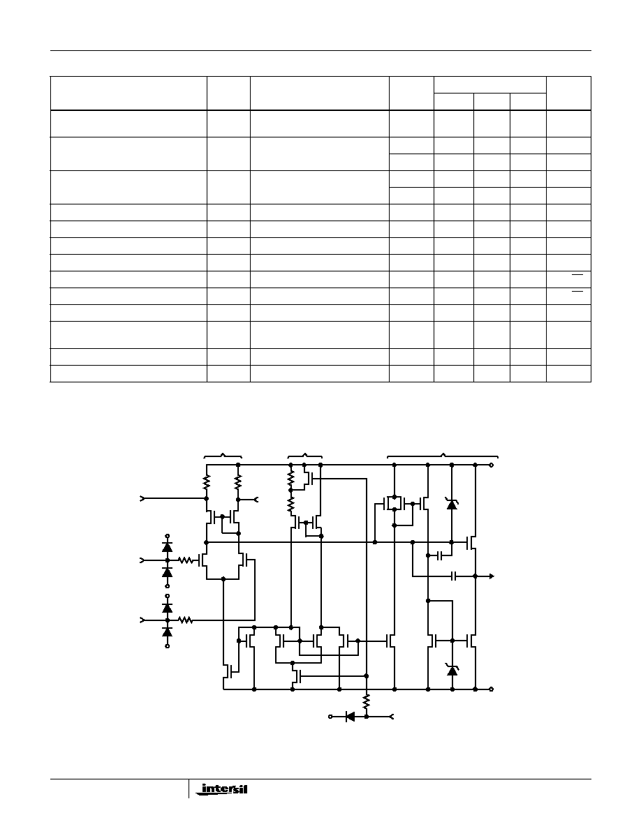
Schematic Diagram
Extended Common Mode
Voltage Range (ICL7612 Only)
V
CMR
25
+0.6 to
-1.1
-
-
V
Output Voltage Swing
V
OUT
R
L
= 1M
25
±
0.98
-
-
V
Full
±
0.96
-
-
V
Large Signal Voltage Gain
A
VOL
V
O
=
±
0.1V, R
L
= 1M
25
-
90
-
dB
Full
-
80
-
dB
Unity Gain Bandwidth
GBW
25
-
0.044
-
MHz
Input Resistance
R
IN
25
-
10
12
-
Common Mode Rejection Ratio
CMRR
R
S
100k
25
-
80
-
dB
Power Supply Rejection Ratio
PSRR
R
S
100k
25
-
80
-
dB
Input Referred Noise Voltage
e
N
R
S
= 100
, f = 1kHz
25
-
100
-
nV/
Hz
Input Referred Noise Current
i
N
R
S
= 100
, f = 1kHz
25
-
0.01
-
pA/
Hz
Supply Current
I
SUPPLY
No Signal, No Load
25
-
6
15
µ
A
Slew Rate
SR
A
V
= 1, C
L
= 100pF,
V
IN
= 0.2V
P-P
, R
L
= 1M
25
-
0.016
-
V/
µ
s
Rise Time
t
r
V
IN
= 50mV, C
L
= 100pF R
L
= 1M
25
-
20
-
µ
s
Overshoot Factor
OS
V
IN
= 50mV, C
L
= 100pF, R
L
= 1M
25
-
5
-
%
Electrical Specifications
V
SUPPLY
=
±
1V, I
Q
= 10
µ
A, Unless Otherwise Specified (Continued)
PARAMETER
SYMBOL
TEST
CONDITIONS
TEMP
(
o
C)
ICL7611B, ICL7612B
UNITS
MIN
TYP
MAX
INPUT STAGE
SETTING STAGE
I
Q
OUTPUT STAGE
V+
OUTPUT
V-
Q
N11
Q
N10
Q
N9
C
FF
= 9pF
C
C
= 33pF
Q
P9
Q
P8
Q
P7
Q
P6
6.3V
Q
N7
Q
N6
Q
N5
Q
N4
V+
I
Q
SET
Q
N8
Q
N3
Q
N1
Q
N2
Q
P1
Q
P1
3K
3K
BAL
100K
900K
Q
P5
Q
P4
Q
P3
+INPUT
-INPUT
V-
V-
V+
V+
BAL
6.3V
ICL7611, ICL7612
5
Application Information
Static Protection
All devices are static protected by the use of input diodes.
However, strong static fields should be avoided, as it is
possible for the strong fields to cause degraded diode
junction characteristics, which may result in increased input
leakage currents.
Latchup Avoidance
Junction-isolated CMOS circuits employ configurations which
produce a parasitic 4-layer (PNPN) structure. The 4-layer
structure has characteristics similar to an SCR, and under
certain circumstances may be triggered into a low impedance
state resulting in excessive supply current. To avoid this
condition, no voltage greater than 0.3V beyond the supply
rails may be applied to any pin. In general, the op amp
supplies must be established simultaneously with, or before
any input signals are applied. If this is not possible, the drive
circuits must limit input current flow to 2mA to prevent latchup.
Choosing the Proper I
Q
The ICL7611 and ICL7612 have a similar I
Q
set-up scheme,
which allows the amplifier to be set to nominal quiescent
currents of 10
µ
A, 100
µ
A or 1mA. These current settings
change only very slightly over the entire supply voltage
range. The ICL7611/12 have an external I
Q
control terminal,
permitting user selection of quiescent current. To set the I
Q
connect the I
Q
terminal as follows:
I
Q
= 10
µ
A - I
Q
pin to V+
I
Q
= 100
µ
A - I
Q
pin to ground. If this is not possible, any
voltage from V+ - 0.8 to V- +0.8 can be used.
I
Q
= 1mA - I
Q
pin to V-
NOTE: The output current available is a function of the quiescent
current setting. For maximum peak-to-peak output voltage swings
into low impedance loads, IQ of 1mA should be selected.
Output Stage and Load Driving Considerations
Each amplifiers' quiescent current flows primarily in the
output stage. This is approximately 70% of the I
Q
settings.
This allows output swings to almost the supply rails for
output loads of 1M
, 100k
, and 10k
, using the output
stage in a highly linear class A mode. In this mode,
crossover distortion is avoided and the voltage gain is
maximized. However, the output stage can also be operated
in Class AB for higher output currents. (See graphs under
Typical Operating Characteristics). During the transition from
Class A to Class B operation, the output transfer
characteristic is non-linear and the voltage gain decreases.
Input Offset Nulling
Offset nulling may be achieved by connecting a 25K pot
between the BAL terminals with the wiper connected to V+.
At quiescent currents of 1mA and 100
µ
A the nulling range
provided is adequate for all V
OS
selections; however with
I
Q
= 10
µ
A, nulling may not be possible with higher values
of V
OS
.
Frequency Compensation
The ICL7611 and ICL7612 are internally compensated, and
are stable for closed loop gains as low as unity with
capacitive loads up to 100pF.
Extended Common Mode Input Range
The ICL7612 incorporates additional processing which
allows the input CMVR to exceed each power supply rail by
0.1V for applications where V
SUPP
±
1.5V. For those
applications where V
SUPP
±
1.5V the input CMVR is limited
in the positive direction, but may exceed the negative supply
rail by 0.1V in the negative direction (e.g., for V
SUPPLY
=
±
1V,
the input CMVR would be +0.6V to -1.1V).
Operation At V
SUPPLY
=
±
1V
Operation at V
SUPPLY
=
±
1V is guaranteed at I
Q
= 10
µ
A for
A and B grades only.
Output swings to within a few millivolts of the supply rails are
achievable for R
L
1M
. Guaranteed input CMVR is
±
0.6V
minimum and typically +0.9V to -0.7V at V
SUPPLY
=
±
1V. For
applications where greater common mode range is
desirable, refer to the description of ICL7612 above.
Typical Applications
The user is cautioned that, due to extremely high input
impedances, care must be exercised in layout, construction,
board cleanliness, and supply filtering to avoid hum and
noise pickup.
Note that in no case is I
Q
shown. The value of I
Q
must be
chosen by the designer with regard to frequency response
and power dissipation.
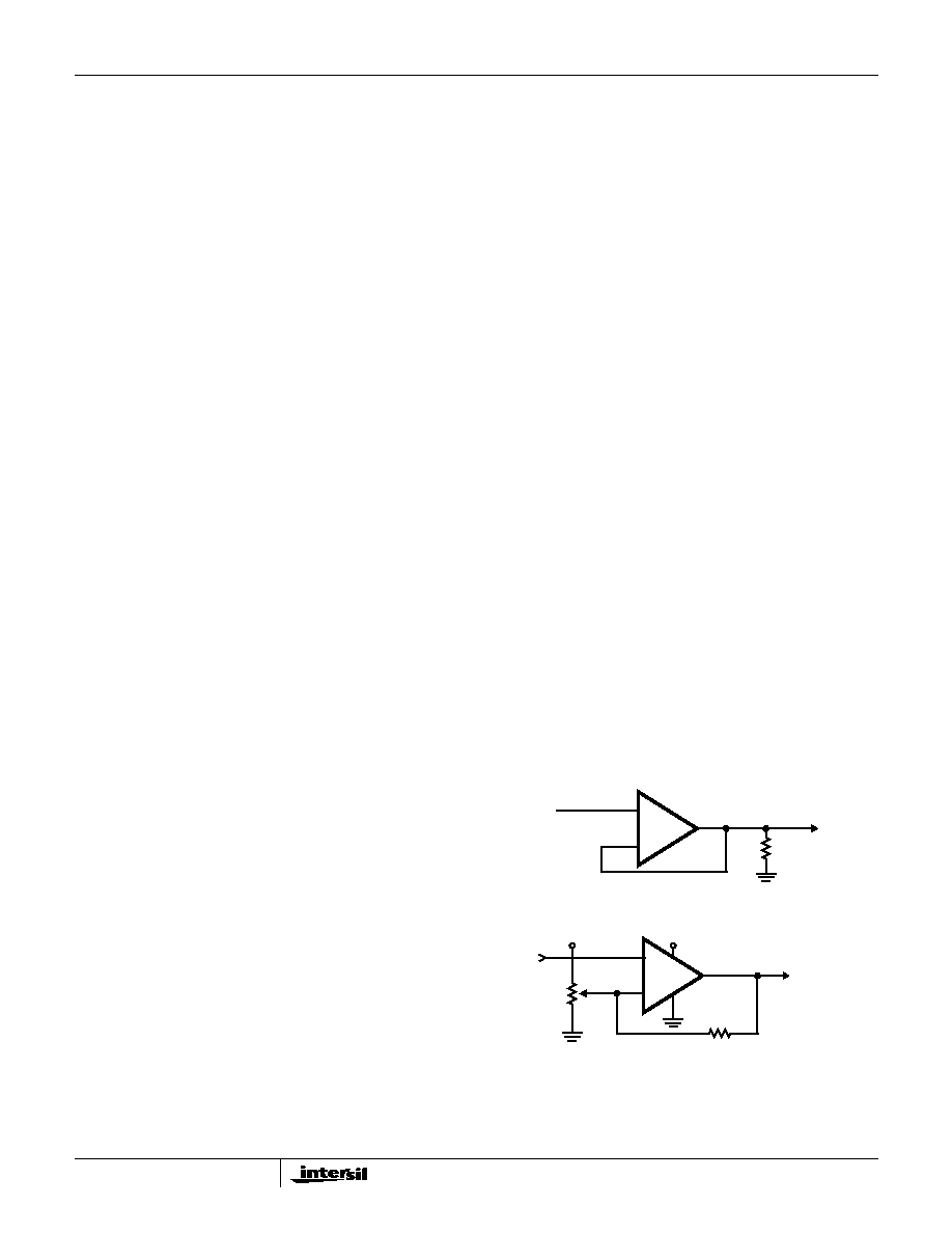
ICL7612
+
-
V
IN
V
OUT
R
L
10K
FIGURE 1. SIMPLE FOLLOWER (NOTE 4)
ICL7612
+
-
V
IN
V
OUT
100K
+5
+5
1M
TO CMOS OR
LPTTL LOGIC
NOTE:
4. By using the ICL7612 in this application, the circuit will follow rail
to rail inputs.
FIGURE 2. LEVEL DETECTOR (NOTE 4)
ICL7611, ICL7612