 | –≠–ª–µ–∫—Ç—Ä–æ–Ω–Ω—ã–π –∫–æ–º–ø–æ–Ω–µ–Ω—Ç: ICL7641C | –°–∫–∞—á–∞—Ç—å:  PDF PDF  ZIP ZIP |
1
File Number
3403.4
ICL7621
Dual, Low Power CMOS Operational
Amplifiers
The ICL761X/762X series is a family of monolithic CMOS
operational amplifiers. These devices provide the designer
with high performance operation at low supply voltages and
selectable quiescent currents. They are an ideal design tool
when ultra low input current and low power dissipation are
desired.
The basic amplifier will operate at supply voltages ranging
from
±
1V to
±
8V, and may be operated from a single Lithium
cell. The output swing ranges to within a few millivolts of the
supply voltages.
The quiescent supply current of these amplifiers is set to
100
µ
A at the factory. This results in power consumption as
low as 200
µ
W per amplifier.
Of particular significance is the extremely low (1pA) input
current, input noise current of 0.01pA/
Hz, and 10
12
input
impedance. These features optimize performance in very
high source impedance applications.
The inputs are internally protected. Outputs are fully
protected against short circuits to ground or to either supply.
Because of the low power dissipation, junction temperature
rise and drift are quite low. Applications utilizing these
features may include stable instruments, extended life
designs, or high density packages.
Features
∑ Wide Operating Voltage Range . . . . . . . . . . .
±
1V to
±
8V
∑ High Input Impedance . . . . . . . . . . . . . . . . . . . . . . . 10
12
∑ Input Current Lower Than BIFETs . . . . . . . . . . . 1pA (Typ)
∑ Output Voltage Swing . . . . . . . . . . . . . . . . . . . . V+ and V-
∑ Available as Duals (Refer to ICL7611 for Singles)
∑ Low Power Replacement for Many Standard Op Amps
Applications
∑ Portable Instruments
∑ Telephone Headsets
∑ Hearing Aid/Microphone Amplifiers
∑ Meter Amplifiers
∑ Medical Instruments
∑ High Impedance Buffers
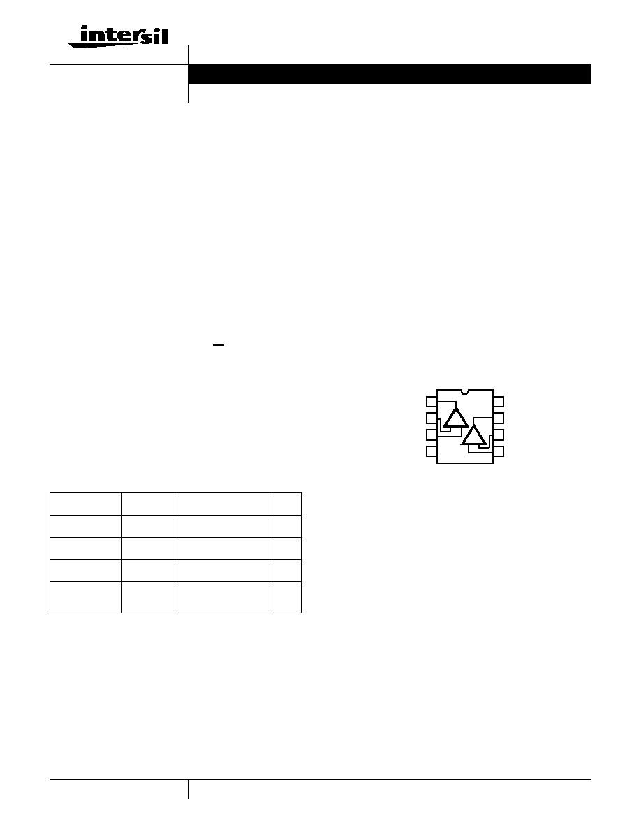
Pinouts
ICL7621 (PDIP, SOIC)
TOP VIEW
Ordering Information
PART NUMBER
TEMP.
RANGE (
o
C)
PACKAGE
PKG.
NO.
ICL7621BCPA
0 to 70
8 Ld PDIP -
B Grade - I
Q
= 100
µ
A
E8.3
ICL7621DCPA
0 to 70
8 Ld PDIP -
D Grade - I
Q
= 100
µ
A
E8.3
ICL7621DCBA
0 to 70
8 Ld SOIC -
D Grade - I
Q
= 100
µ
A
M8.15
ICL7621DCBA-T
0 to 70
8 Ld SOIC - D Grade -
Tape and Reel -
I
Q
= 100
µ
A
M8.15
OUT
A
-IN
A
+IN
A
V-
1
2
3
4
8
7
6
5
V+
OUT
B
-IN
B
+IN
B
+
-
+
-
Data Sheet
May 2001
Title
CL76
,
L76
,
L76
)
ub-
ct
ual/
uad,
w
wer
MOS
pera-
nal
mpli-
rs)
utho
)
ey-
ords
nter-
l
orpo-
tion,
mi-
n-
ctor,
al,
ad,
era-
nal
pli-
CAUTION: These devices are sensitive to electrostatic discharge; follow proper IC Handling Procedures.
1-888-INTERSIL or 321-724-7143
|
Intersil and Design is a trademark of Intersil Americas Inc.
|
Copyright © Intersil Americas Inc. 2001
2
Absolute Maximum Ratings
Thermal Information
Supply Voltage V+ to V- . . . . . . . . . . . . . . . . . . . . . . . . . . . . . . . .18V
Input Voltage . . . . . . . . . . . . . . . . . . . . . . . . . . . V- -0.3 to V+ +0.3V
Differential Input Voltage (Note 1) . . . . . . . . . [(V+ +0.3) - (V- -0.3)]V
Duration of Output Short Circuit (Note 2). . . . . . . . . . . . . . Unlimited
Operating Conditions
Temperature Range
ICL7621C . . . . . . . . . . . . . . . . . . . . . . . . . . . . . . . . . 0
o
C to 70
o
C
Thermal Resistance (Typical, Note 3)
JA
(
o
C/W)
JC
(
o
C/W)
PDIP Package . . . . . . . . . . . . . . . . . . .
120
N/A
SOIC Package . . . . . . . . . . . . . . . . . . .
160
N/A
Maximum Junction Temperature (Plastic Package) . . . . . . . . 150
o
C
Maximum Storage Temperature Range . . . . . . . . . . -65
o
C to 150
o
C
Maximum Lead Temperature (Soldering 10s) . . . . . . . . . . . . 300
o
C
(SOIC - Lead Tips Only)
CAUTION: Stresses above those listed in "Absolute Maximum Ratings" may cause permanent damage to the device. This is a stress only rating and operation of the
device at these or any other conditions above those indicated in the operational sections of this specification is not implied.
NOTES:
1. Long term offset voltage stability will be degraded if large input differential voltages are applied for long periods of time.
2. The outputs may be shorted to ground or to either supply, for V
SUPPLY
10V. Care must be taken to insure that the dissipation rating is not
exceeded.
3.
JA
is measured with the component mounted on an evaluation PC board in free air.
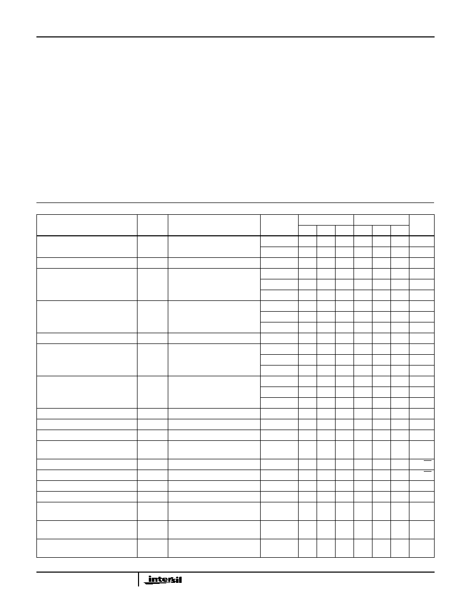
Electrical Specifications
V
SUPPLY
=
±
5V, Unless Otherwise Specified
PARAMETER
SYMBOL
TEST CONDITIONS
TEMP. (
o
C)
ICL7621B
ICL7621D
UNITS
MIN
TYP MAX
MIN
TYP MAX
Input Offset Voltage
V
OS
R
S
100k
25
-
-
5
-
-
15
mV
Full
-
-
7
-
-
20
mV
Temperature Coefficient of V
OS
V
OS
/
T R
S
100k
-
-
15
-
-
25
-
µ
V/
o
C
Input Offset Current
I
OS
25
-
0.5
30
-
0.5
30
pA
0 to 70
-
-
300
-
-
300
pA
-55 to 125
-
800
-
800
pA
Input Bias Current
I
BIAS
25
-
1.0
50
-
1.0
50
pA
0 to 70
-
-
400
-
-
400
pA
-55 to 125
-
-
4000
-
-
4000
pA
Common Mode Voltage Range
V
CMR
I
Q
= 100
µ
A
25
±
4.2
-
-
±
4.2
-
-
V
Output Voltage Swing
V
OUT
I
Q
= 100
µ
A, R
L
= 100k
25
±
4.9
-
-
±
4.9
-
-
V
0 to 70
±
4.8
-
-
±
4.8
-
-
V
-55 to 125
±
4.5
-
-
±
4.5
-
-
V
Large Signal
Voltage Gain
A
VOL
V
O
=
±
4.0V, R
L
= 100k
,
I
Q
= 100
µ
A
25
80
102
-
80
102
-
dB
0 to 70
75
-
-
75
-
-
dB
-55 to 125
68
-
-
68
-
-
dB
Unity Gain Bandwidth
GBW
I
Q
= 100
µ
A
25
-
0.48
-
-
0.48
-
MHz
Input Resistance
R
IN
25
-
10
12
-
-
10
12
-
Common Mode Rejection Ratio
CMRR
R
S
100k
,
I
Q
= 100
µ
A
25
70
91
-
70
91
-
dB
Power Supply Rejection Ratio
(V
SUPPLY
=
±
8V to
±
2V)
PSRR
R
S
100k
,
I
Q
= 100
µ
A
25
80
86
-
80
86
-
dB
Input Referred Noise Voltage
e
N
R
S
= 100
, f = 1kHz
25
-
100
-
-
100
-
nV/
Hz
Input Referred Noise Current
i
N
R
S
= 100
, f = 1kHz
25
-
0.01
-
-
0.01
-
pA/
Hz
Supply Current (Per Amplifier)
I
SUPPLY
No Signal, No Load, I
Q
= 100
µ
A
25
-
0.1
0.25
-
0.1
0.25
mA
Channel Separation
V
O1
/V
O2
A
V
= 100
25
-
120
-
-
120
-
dB
Slew Rate
SR
A
V
= 1, C
L
= 100pF, V
IN
= 8V
P-P
,
I
Q
= 100
µ
A, R
L
= 100k
25
-
0.16
-
-
0.16
-
V/
µ
s
Rise Time
t
R
V
IN
= 50mV, C
L
= 100pF,
I
Q
= 100
µ
A, R
L
= 100k
25
-
2
-
-
2
-
µ
s
Overshoot Factor
OS
V
IN
= 50mV, C
L
= 100pF,
I
Q
= 100
µ
A, R
L
= 100k
25
-
10
-
-
10
-
%
ICL7621
3
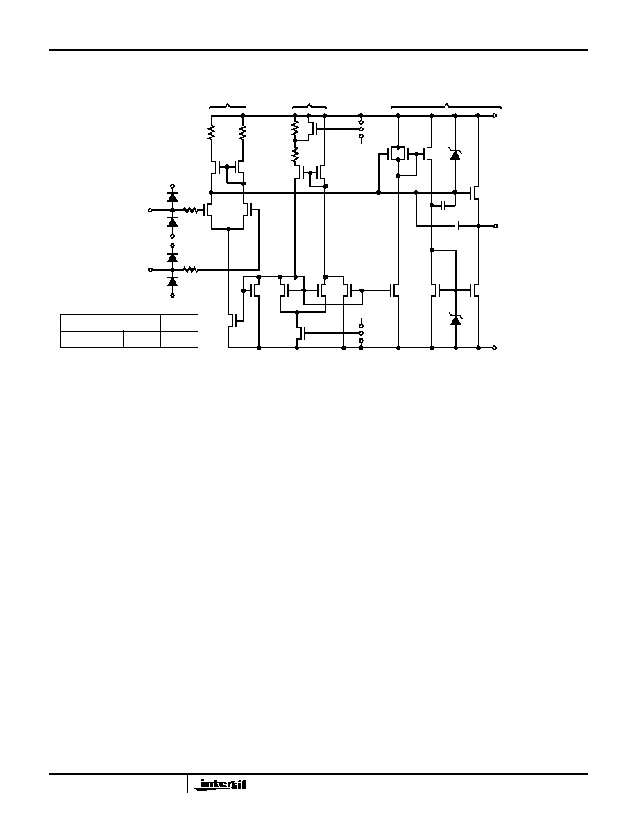
Schematic Diagram
Application Information
Static Protection
All devices are static protected by the use of input diodes.
However, strong static fields should be avoided, as it is
possible for the strong fields to cause degraded diode
junction characteristics, which may result in increased input
leakage currents.
Latchup Avoidance
Junction-isolated CMOS circuits employ configurations
which produce a parasitic 4-layer (PNPN) structure. The
4-layer structure has characteristics similar to an SCR, and
under certain circumstances may be triggered into a low
impedance state resulting in excessive supply current. To
avoid this condition, no voltage greater than 0.3V beyond the
supply rails may be applied to any pin. In general, the op
amp supplies must be established simultaneously with, or
before any input signals are applied. If this is not possible,
the drive circuits must limit input current flow to 2mA to
prevent latchup.
Choosing the Proper I
Q
Each device in the ICL76XX family has a similar I
Q
setup
scheme, which allows the amplifier to be set to nominal
quiescent currents of 10
µ
A, 100
µ
A or 1mA. These current
settings change only very slightly over the entire supply
voltage range. The ICL7611/12 have an external I
Q
control
terminal, permitting user selection of each amplifiers'
quiescent current. The ICL7621 has a fixed I
Q
setting of
100
µ
A.
Output Stage and Load Driving Considerations
Each amplifiers' quiescent current flows primarily in the
output stage. This is approximately 70% of the I
Q
settings.
This allows output swings to almost the supply rails for
output loads of 1M
, 100k
, and 10k
, using the output
stage in a highly linear class A mode. In this mode,
crossover distortion is avoided and the voltage gain is
maximized. However, the output stage can also be operated
in Class AB for higher output currents. (See graphs under
Typical Operating Characteristics). During the transition from
Class A to Class B operation, the output transfer
characteristic is nonlinear and the voltage gain decreases.
Frequency Compensation
The ICL76XX are internally compensated, and are stable
for closed loop gains as low as unity with capacitive loads
up to 100pF.
INPUT STAGE
SETTING STAGE
I
Q
OUTPUT STAGE
V+
OUTPUT
V-
Q
N11
Q
N10
Q
N9
C
FF
= 9pF
C
C
= 33pF
Q
P9
Q
P8
Q
P7
Q
P6
6.3V
Q
N7
Q
N6
Q
N5
Q
N4
Q
N8
Q
N3
Q
N1
Q
N2
Q
P1
Q
P2
3K
3K
100K
900K
Q
P5
Q
P4
Q
P3
+INPUT
-INPUT
V-
V-
V+
V+
A
C
V-
G
E
V+
TABLE OF JUMPERS
I
Q
ICL7621
C, E
100
µ
A
6.3V
ICL7621
4
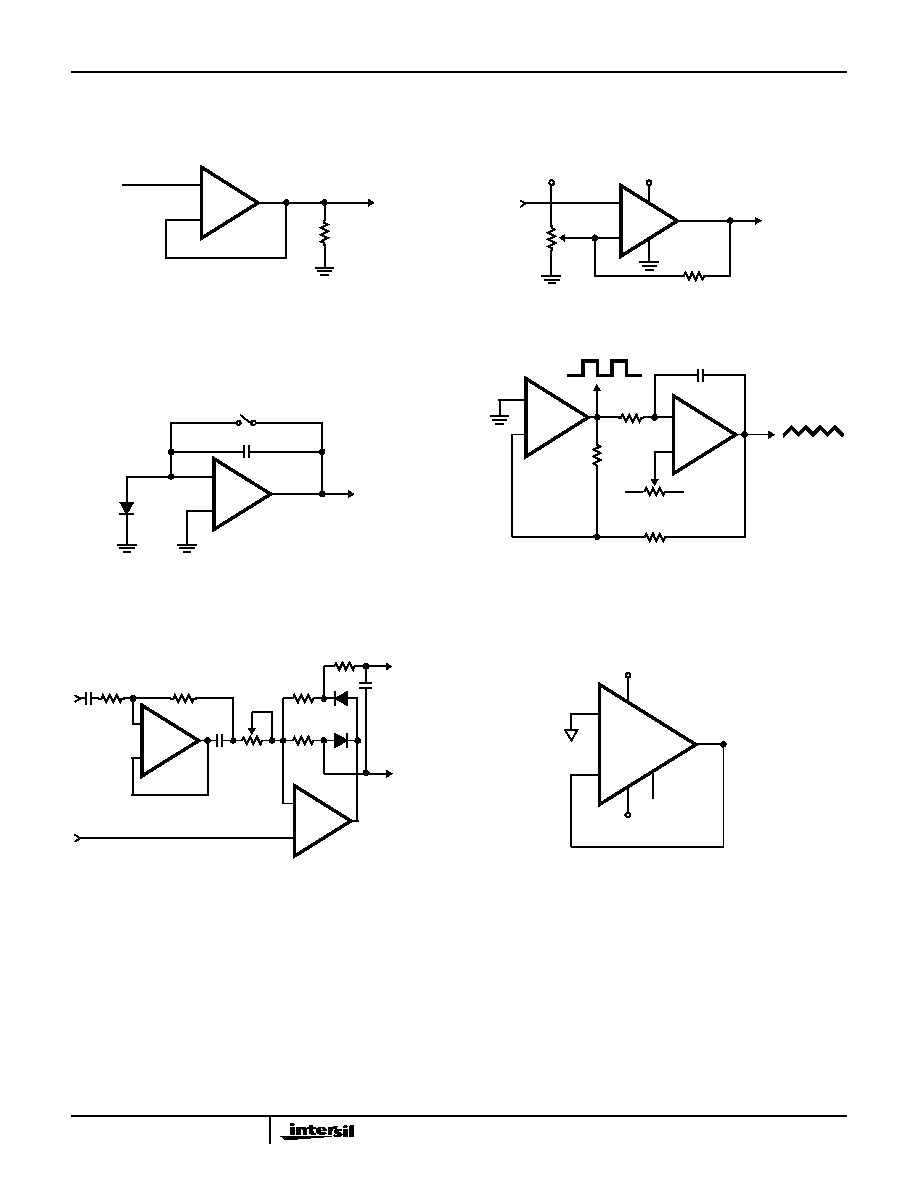
Typical Applications
The user is cautioned that, due to extremely high input
impedances, care must be exercised in layout, construction,
board cleanliness, and supply filtering to avoid hum and
noise pickup.
FIGURE 1. SIMPLE FOLLOWER
FIGURE 2. LEVEL DETECTOR
FIGURE 3. PHOTOCURRENT INTEGRATOR
FIGURE 4. TRIANGLE/SQUARE WAVE GENERATOR
FIGURE 5. AVERAGING AC TO DC CONVERTER FOR A/D
CONVERTERS SUCH AS ICL7106, ICL7107,
ICL7109, ICL7116, ICL7117
FIGURE 6. BURN-IN AND LIFE TEST CIRCUIT
ICL76XX
+
-
V
IN
V
OUT
R
L
10k
ICL76XX
+
-
V
IN
V
OUT
100k
+5
+5
1M
TO CMOS OR
LPTTL LOGIC
V
OUT
1
µ
F
ICL76XX
+
-
+
NOTE: Low leakage currents allow integration times up to
several hours.
1M
+
-
1M
DUTY CYCLE
V-
V+
680k
1M
WAVEFORM GENERATOR
+
-
1/2
ICL7621
1/2
ICL7621
NOTE: Since the output range swings exactly from rail to rail, fre-
quency and duty cycle are virtually independent of power supply
variations.
10
µ
F
1/2
+
-
20k
V
IN
20k
V
OH
V
OL
1M
2.2M
COMMON
10k
0.5
µ
F
1.8k = 5%
SCALE
ADJUST
TO
SUCCEEDING
INPUT
STAGE
+
-
ICL7621
1/2
ICL7621
+
-
V-
OUT
V+
V+
-8V
+8V
T
A
= 125
o
C
ICL7621
5
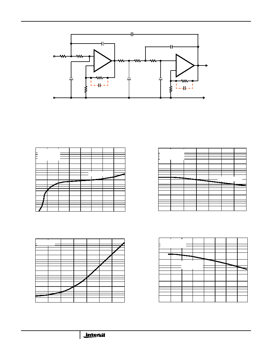
FIGURE 7. FIFTH ORDER CHEBYCHEV MULTIPLE FEEDBACK LOW PASS FILTER
+
-
+
-
INPUT
30k
160k
0.2
µ
F
0.2
µ
F
0.2
µ
F
0.2
µ
F
0.1
µ
F
0.1
µ
F
51k
100k
680k
360k
360k
1M
1M
OUTPUT
1/2
ICL7621
1/2
ICL7621
NOTE 4
NOTE 4
NOTES:
4. Small capacitors (25 - 50pF) may be needed for stability in some cases.
5. The low bias currents permit high resistance and low capacitance values to be used to achieve low frequency cutoff. f
C
= 10Hz, AV
CL
= 4,
Passband ripple = 0.1dB.
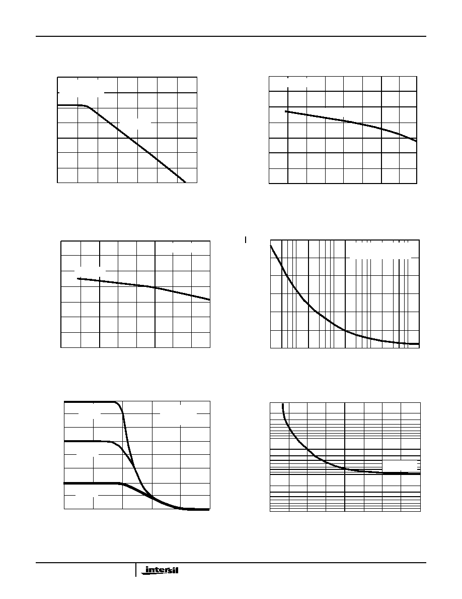
Typical Performance Curves
FIGURE 8. SUPPLY CURRENT PER AMPLIFIER vs SUPPLY
VOLTAGE
FIGURE 9. SUPPLY CURRENT PER AMPLIFIER vs FREE-AIR
TEMPERATURE
FIGURE 10. INPUT BIAS CURRENT vs TEMPERATURE
FIGURE 11. LARGE SIGNAL DIFFERENTIAL VOLTAGE GAIN
vs FREE-AIR TEMPERATURE
10K
1K
100
10
1
S
U
P
P
L
Y
CURRE
NT
(
µ
A)
0
2
4
6
8
10
12
14
16
SUPPLY VOLTAGE (V)
T
A
= 25
o
C
NO LOAD
NO SIGNAL
I
Q
= 100
µ
A
10
4
10
3
10
2
10
1
S
U
P
P
L
Y
CURRE
NT
(
µ
A)
-50
-25
0
25
50
75
100
125
FREE-AIR TEMPERATURE (
o
C)
V+ - V- = 10V
NO LOAD
NO SIGNAL
I
Q
= 100
µ
A
-50
-25
0
25
50
75
100
125
FREE-AIR TEMPERATURE (
o
C)
1000
100
10
1.0
0.1
INP
U
T
B
IAS
CURRE
NT
(
p
A)
V
S
=
±
5V
-50
-25
0
25
50
75
100
125
FREE-AIR TEMPERATURE (
o
C)
-75
1000
100
10
1
DIF
F
E
RE
NT
IAL
V
O
L
T
A
G
E
G
A
I
N
(
k
V
/
V
)
V
SUPPLY
= 10V
V
OUT
= 8V
R
L
= 100k
I
Q
= 100
µ
A
ICL7621
6
FIGURE 12. LARGE SIGNAL FREQUENCY RESPONSE
FIGURE 13. COMMON MODE REJECTION RATIO vs FREE-AIR
TEMPERATURE
FIGURE 14. POWER SUPPLY REJECTION RATIO vs FREE-AIR
TEMPERATURE
FIGURE 15. EQUIVALENT INPUT NOISE VOLTAGE vs
FREQUENCY
FIGURE 16. OUTPUT VOLTAGE vs FREQUENCY
FIGURE 17. OUTPUT SINK CURRENT vs SUPPLY VOLTAGE
Typical Performance Curves
(Continued)
10
7
10
6
10
4
10
3
10
2
10
1
10
5
DIF
F
E
RE
NT
IAL
V
O
L
T
A
G
E
G
A
IN
(
V
/V
)
0.1
1.0
10
100
1K
10K
100K
1M
FREQUENCY (Hz)
T
A
= 25
o
C
V
SUPPLY
= 15V
I
Q
= 100
µ
A
-50
-25
0
25
50
75
100
125
FREE-AIR TEMPERATURE (
o
C)
-75
105
100
95
90
85
80
75
70
CO
M
M
O
N
M
O
DE
RE
J
E
CT
IO
N
R
A
T
IO
(
d
B)
V
SUPPLY
= 10V
I
Q
= 100
µ
A
100
95
90
85
80
75
70
65
S
U
P
P
L
Y
V
O
L
T
A
G
E
RE
J
E
CT
IO
N
R
A
T
IO
(
d
B)
-50
-25
0
25
50
75
100
125
-75
FREE-AIR TEMPERATURE (
o
C)
I
Q
= 100
µ
A
V
SUPPLY
= 10V
600
500
400
300
200
100
0
EQ
U
I
V
A
L
E
N
T
I
N
PU
T
N
O
I
SE
VO
L
T
A
G
E
(
n
V/
Hz
)
10
100
1K
10K
100K
FREQUENCY (Hz)
T
A
= 25
o
C
3V
V
SUPPLY
16V
16
14
12
10
8
6
4
2
0
MA
X
I
MU
M
P
E
A
K
-
T
O
-
P
E
A
K
O
U
T
P
UT
V
O
L
T
AG
E
(
V
P-
P
)
100
1K
10K
100K
1M
10M
FREQUENCY (Hz)
V
SUPPLY
=
±
8V
V
SUPPLY
=
±
5V
V
SUPPLY
=
±
2V
I
Q
= 100
µ
A
T
A
= 25
o
C
0.01
0.1
1.0
10
M
A
X
I
M
U
M
O
UT
P
U
T
S
INK
CURRE
NT
(
m
A)
0
2
4
6
8
10
12
14
16
SUPPLY VOLTAGE (V)
I
Q
= 100
µ
A
ICL7621
7
All Intersil products are manufactured, assembled and tested utilizing ISO9000 quality systems.
Intersil Corporation's quality certifications can be viewed at website www.intersil.com/design/quality/iso.asp
Intersil products are sold by description only. Intersil Corporation reserves the right to make changes in circuit design and/or specifications at any time without notice.
Accordingly, the reader is cautioned to verify that data sheets are current before placing orders. Information furnished by Intersil is believed to be accurate and reliable. How-
ever, no responsibility is assumed by Intersil or its subsidiaries for its use; nor for any infringements of patents or other rights of third parties which may result from its use.
No license is granted by implication or otherwise under any patent or patent rights of Intersil or its subsidiaries.
For information regarding Intersil Corporation and its products, see web site www.intersil.com
Sales Office Headquarters
NORTH AMERICA
Intersil Corporation
2401 Palm Bay Rd.
Palm Bay, FL 32905
TEL: (321) 724-7000
FAX: (321) 724-7240
EUROPE
Intersil SA
Mercure Center
100, Rue de la Fusee
1130 Brussels, Belgium
TEL: (32) 2.724.2111
FAX: (32) 2.724.22.05
ASIA
Intersil Ltd.
8F-2, 96, Sec. 1, Chien-kuo North,
Taipei, Taiwan 104
Republic of China
TEL: 886-2-2515-8508
FAX: 886-2-2515-8369
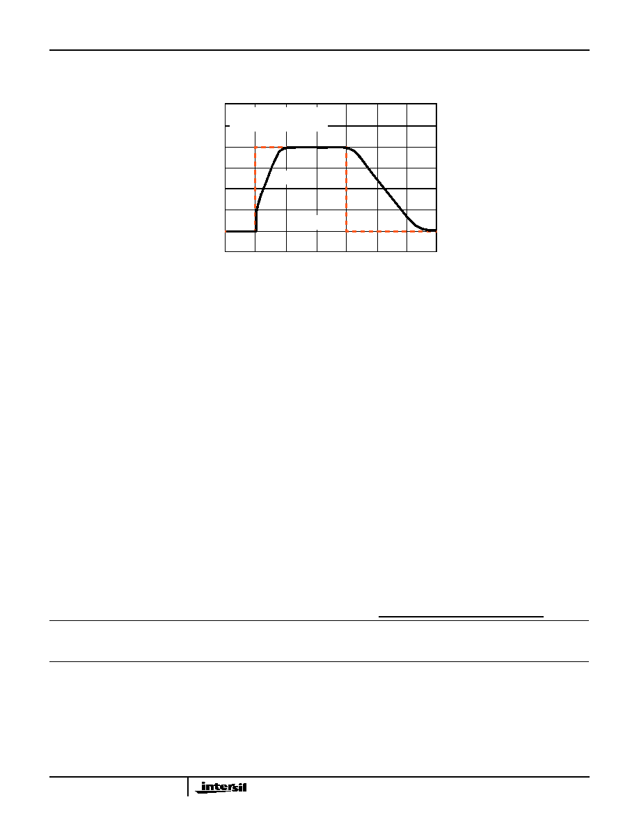
FIGURE 18. VOLTAGE FOLLOWER LARGE SIGNAL PULSE RESPONSE (I
Q
= 100
µ
A)
Typical Performance Curves
(Continued)
8
6
4
2
0
-2
-4
-6
I
N
PU
T
A
N
D
O
U
T
P
U
T
VO
L
T
A
G
E
(
V
)
0
20
40
60
80
100
120
TIME (
µ
s)
T
A
= 25
o
C, V
SUPPLY
= 10V
R
L
= 100k
, C
L
= 100pF
OUTPUT
INPUT
ICL7621