55
TM
File Number 3180.3
ICL7663S
CMOS Programmable Micropower
Positive Voltage Regulator
The ICL7663S Super Programmable Micropower Voltage
Regulator is a low power, high efficiency positive voltage
regulator which accepts 1.6V to 16V inputs and provides
adjustable outputs from 1.3V to 16V at currents up to 40mA.
It is a direct replacement for the industry standard ICL7663B
offering wider operating voltage and temperature ranges,
improved output accuracy (ICL7663SA), better temperature
coefficient, guaranteed maximum supply current, and
guaranteed line and load regulation. All improvements are
highlighted in the electrical characteristics section. Critical
parameters are guaranteed over the entire commercial
and industrial temperature ranges. The ICL7663S/SA
programmable output voltage is set by two external resistors.
The 1% reference accuracy of the ICL7663SA eliminates the
need for trimming the output voltage in most applications.
The ICL7663S is well suited for battery powered supplies,
featuring 4
µ
A quiescent current, low V
IN
to V
OUT
differential,
output current sensing and logic input level shutdown
control. In addition, the ICL7663S has a negative
temperature coefficient output suitable for generating a
temperature compensated display drive voltage for LCD
displays.
Features
∑ Guaranteed 10
µ
A Maximum Quiescent Current Over All
Temperature Ranges
∑ Wider Operating Voltage Range - 1.6V to 16V
∑ Guaranteed Line and Load Regulation Over Entire
Operating Temperature Range Optional
∑ 1% Output Voltage Accuracy (ICL7663SA)
∑ Output Voltage Programmable from 1.3V to 16V
∑ Improved Temperature Coefficient of Output Voltage
∑ 40mA Minimum Output Current with Current Limiting
∑ Output Voltages with Programmable Negative
Temperature Coefficients
∑ Output Shutdown via Current-Limit Sensing or External
Logic Level
∑ Low Input-to-Output Voltage Differential
∑ Improved Direct Replacement for Industry Standard
ICL7663B and Other Second-Source Products
Applications
∑ Low-Power Portable Instrumentation
∑ Pagers
∑ Handheld Instruments
∑ LCD Display Modules
∑ Remote Data Loggers
∑ Battery-Powered Systems
Pinout
ICL7663S
(PDIP, CERDIP, SOIC)
TOP VIEW
Ordering Information
PART NUMBER
TEMP. RANGE
(
o
C)
PACKAGE
PKG. NO.
ICL7663SCBA
0
to 70
8 Ld SOIC (N)
M8.15
ICL7663SCPA
0
to 70
8 Ld PDIP
E8.3
ICL7663SACBA
0
to 70
8 Ld SOIC (N)
M8.15
ICL7663SACPA
0
to 70
8 Ld PDIP
E8.3
ICL7663SIBA
-25
to 85
8 Ld SOIC (N)
M8.15
ICL7663SIPA
-25
to 85
8 Ld PDIP
E8.3
ICL7663SAIBA
-25
to 85
8 Ld SOIC (N)
M8.15
ICL7663SAIPA
-25
to 85
8 Ld PDIP
E8.3
SENSE
V
OUT2
V
OUT1
GND
1
2
3
4
8
7
6
5
V
IN
+
V
TC
V
SET
SHDN
Data Sheet
April 1999
CAUTION: These devices are sensitive to electrostatic discharge; follow proper IC Handling Procedures.
1-888-INTERSIL or 321-724-7143
|
Intersil (and design) is a trademark of Intersil Americas Inc.
Copyright © Intersil Americas Inc. 2001. All Rights Reserved

56
Absolute Maximum Ratings
Thermal Information
Input Supply Voltage . . . . . . . . . . . . . . . . . . . . . . . . . . . . . . . . .+18V
Any Input or Output Voltage (Note 1)
Terminals 1, 2, 3, 5, 6, 7. . . . . . . . . . . . . V
IN
+ 0.3V to GND -0.3V
Output Source Current
Terminal 2 . . . . . . . . . . . . . . . . . . . . . . . . . . . . . . . . . . . . . . 50mA
Terminal 3 . . . . . . . . . . . . . . . . . . . . . . . . . . . . . . . . . . . . . . 25mA
Output Sinking Current
Terminal 7 . . . . . . . . . . . . . . . . . . . . . . . . . . . . . . . . . . . . . -10mA
Operating Conditions
Temperature Range
ICL7663SC. . . . . . . . . . . . . . . . . . . . . . . . . . . . . . . . . 0
o
C to 70
o
C
ICL7663SI . . . . . . . . . . . . . . . . . . . . . . . . . . . . . . . -25
o
C to 85
o
C
Thermal Resistance (Typical, Note 2)
JA
(
o
C/W)
JC
(
o
C/W)
CERDIP Package. . . . . . . . . . . . . . . . .
115
30
PDIP Package . . . . . . . . . . . . . . . . . . .
150
N/A
Plastic SOIC Package . . . . . . . . . . . . .
180
N/A
Maximum Junction Temperature
PDIP Package . . . . . . . . . . . . . . . . . . . . . . . . . . . . . . . . . 150
o
C
CERDIP Package. . . . . . . . . . . . . . . . . . . . . . . . . . . . . . . 175
o
C
Maximum Storage Temperature Range . . . . . . . . . -65
o
C to 150
o
C
Maximum Lead Temperature (Soldering 10s) . . . . . . . . . . . . . 300
o
C
(SOIC - Lead Tips Only)
CAUTION: Stresses above those listed in "Absolute Maximum Ratings" may cause permanent damage to the device. This is a stress only rating and operation of the
device at these or any other conditions above those indicated in the operational sections of this specification is not implied.
NOTES:
1. Connecting any terminal to voltages greater than (V+
IN
+ 0.3V) or less than (GND - 0.3V) may cause destructive device latch-up. It is recom-
mended that no inputs from sources operating on external power supplies be applied prior to ICL7663S power-up.
2.
JA
is measured with the component mounted on an evaluation PC board in free air.
Electrical Specifications
Specifications Below Applicable to Both ICL7663S and ICL7663SA, Unless Otherwise Specified. V+
IN
= 9V,
V
OUT
= 5V, T
A
= 25
o
C, Unless Otherwise Specified. Notes 4, 5. See Test Circuit, Figure 7
PARAMETER
SYMBOL
TEST CONDITIONS
MIN
TYP
MAX
UNITS
Input Voltage
V+
IN
ICL7663S
T
A
= 25
o
C
1.5
-
16
V
0
o
C < T
A
< 70
o
C
1.6
-
16
V
-25
o
C < T
A
< 85
o
C
1.6
-
16
V
ICL7663SA
0
o
C < T
A
< 70
o
C
1.6
-
16
V
-25
o
C < T
A
< 85
o
C
1.6
-
16
V
Quiescent Current
I
Q
1.4V
V
OUT
8.5V, No Load
V+
IN
= 9V
0
o
C < T
A
< 70
o
C
-
-
10
µ
A
-25
o
C < T
A
< 85
o
C
-
-
10
µ
A
V+
IN
= 16V
0
o
C < T
A
< 70
o
C
-
-
12
µ
A
-25
o
C < T
A
< 85
o
C
-
-
12
µ
A
Reference Voltage
V
SET
I
OUT1
= 100
µ
A, V
OUT
= V
SET
ICL7663S
T
A
= 25
o
C
1.2
1.3
1.4
V
ICL7663SA
T
A
= 25
o
C
1.275
1.29
1.305
V
Temperature
Coefficient
V
SET
T
0
o
C < T
A
< 70
o
C
-
100
-
ppm
-25
o
C < T
A
< 85
o
C
-
100
-
ppm
Line Regulation
V
SET
V
SET'
V
IN
2V < V
IN
< 15V
0
o
C < T
A
< 70
o
C
-
0.03
-
%/V
-25
o
C < T
A
< 85
o
C
-
0.03
0.3
%/V
V
SET
Input Current
I
SET
0
o
C < T
A
< 70
o
C
-
0.01
10
nA
-25
o
C < T
A
< 85
o
C
-
0.01
10
nA
Shutdown Input Current
I
SHDN
-
±
0.01
10
nA
Shutdown Input Voltage
V
SHDN
V
SHDN
HI: Both V
OUT
Disabled
1.4
-
-
V
V
SHDN
LO: Both V
OUT
Enable
-
-
0.3
V
Sense Pin Input Current
I
SENSE
-
0.01
10
nA
Sense Pin Input Threshold
V
CL
-
0.5
-
V
ICL7663S

57
Functional Diagram
Input-Output Saturation
Resistance (Note 3)
R
SAT
V+
IN
= 2V, I
OUT1
= 1mA
-
170
350
V+
IN
= 9V, I
OUT1
= 2mA
-
50
100
V+
IN
= 15V, I
OUT1
= 5mA
-
35
70
Load Regulation
V
OUT
I
OUT
1mA < I
OUT2
< 20mA
-
1
3
50
µ
A < I
OUT1
< 5mA
-
2
10
Available Output Current
(V
OUT2
)
I
OUT2
3V
V
IN
16V, V
IN
- V
OUT2
= 1.5V
40
-
-
mA
Negative Tempco Output
(Note 4)
V
TC
Open Circuit Voltage
-
0.9
-
V
I
TC
Maximum Sink Current
0
8
2.0
mA
Temperature Coefficient
V
TC
T
Open Circuit
-
+2.5
-
mV/
o
C
Minimum Load Current
I
L(MIN)
Includes V
SET
Divider
T
A
= 25
o
C
-
-
1.0
µ
A
0
o
C < T
A
< 70
o
C
-
0.2
5.0
µ
A
-25
o
C < T
A
< 85
o
C
-
0.2
5.0
µ
A
NOTES:
3. This parameter refers to the saturation resistance of the MOS pass transistor. The minimum input-output voltage differential at low current (under
5mA), can be determined by multiplying the load current (including set resistor current, but not quiescent current) by this resistance.
4. This output has a positive temperature coefficient. Using it in combination with the inverting input of the regulator at V
SET
, a negative
coefficient results in the output voltage. See Figure 9 for details. Pin will not source current.
5. All pins are designed to withstand electrostatic discharge (ESD) levels in excess of 2000V.
6. All significant improvements over the industry standard ICL7663 are highlighted.
Electrical Specifications
Specifications Below Applicable to Both ICL7663S and ICL7663SA, Unless Otherwise Specified. V+
IN
= 9V,
V
OUT
= 5V, T
A
= 25
o
C, Unless Otherwise Specified. Notes 4, 5. See Test Circuit, Figure 7 (Continued)
PARAMETER
SYMBOL
TEST CONDITIONS
MIN
TYP
MAX
UNITS
C
REF
B
A
V
OUT1
V
OUT2
SENSE
V
SET
V
TC
SHUTDOWN
GND
3
2
1
6
7
5
4
V+
IN
8
GND
ICL7663S
58
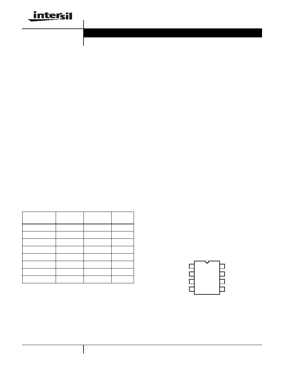
Typical Performance Curves
FIGURE 1. V
OUT2
OUTPUT VOLTAGE AS A FUNCTION OF
OUTPUT CURRENT
FIGURE 2. V
OUT1
INPUT-OUTPUT DIFFERENTIAL vs
OUTPUT CURRENT
FIGURE 3. V
OUT2
INPUT-OUTPUT DIFFERENTIAL vs
OUTPUT CURRENT
FIGURE 4. NPUT POWER SUPPLY REJECTION RATIO
FIGURE 5. QUIESCENT CURRENT AS A FUNCTION OF
INPUT VOLTAGE
FIGURE 6. QUIESCENT CURRENT AS A FUNCTION OF
TEMPERATURE
5.000
4.995
4.990
4.985
4.980
4.975
4.970
4.965
4.960
4.955
4.950
V
OU
T
(V
)
10
-2
10
-1
10
0
10
1
10
2
10
-3
I
OUT
(mA)
T
A
= 25
o
C
V+ = 9.0V
2.0
1.8
1.6
1.4
1.2
1.0
0.8
0.6
0.4
0.2
0
0
2
4
6
8
10
12
14
16
18
20
T
A
= 25
o
C
V+
IN
= 15V
V+
IN
- V
OU
T
1 (
V
)
I
OUT1
(mA)
V+
IN
= 9V
V+
IN
= 2V
I
OUT2
(mA)
V+
IN
-
V
OU
T
1 (
V
)
2.0
1.8
1.6
1.4
1.2
1.0
0.8
0.6
0.4
0.2
0
0
5
10
15
20
25
30
35
40
45
50
V+
IN
= 9V
T
A
= 25
o
C
V+
IN
= 2V
V+
IN
= 15V
10
-2
10
-1
10
0
10
1
10
2
1k
100
90
80
70
60
50
40
30
20
10
0
P
S
RR (
d
B)
FREQUENCY (Hz)
V
IN
= 9.0V
V
IN
= 2V
T
A
= -20
o
C
5.0
4.5
4.0
3.5
3.0
2.5
2.0
1.5
1.0
0.5
0
0
2
4
6
8
10
12
14
16
V+
IN
(V)
I
O
(
µ
A)
T
A
= -25
o
C
T
A
= -70
o
C
5.00
4.75
4.50
4.25
4.00
3.75
3.50
3.25
3.00
2.75
2.50
I
O
(
µ
A)
V+ = 15V
V+ = 9V
V+ = 2V
-20
0
20
40
60
80
TEMPERATURE (
o
C)
ICL7663S

59
Detailed Description
The ICL7663S is a CMOS integrated circuit incorporating all
the functions of a voltage regulator plus protection circuitry
on a single monolithic chip. Referring to the Functional
Diagram, the main blocks are a bandgap-type voltage
reference, an error amplifier, and an output driver with both
PMOS and NPN pass transistors.
The bandgap output voltage, trimmed to 1.29V
±
15mV for
the ICL7663SA, and the input voltage at the V
SET
terminal
are compared in amplifier A. Error amplifier A drives a
P-channel pass transistor which is sufficient for low (under
about 5mA) currents. The high current output is passed by
an NPN bipolar transistor connected as a follower. This
configuration gives more gain and lower output impedance.
Logic-controlled shutdown is implemented via a N-Channel
MOS transistor. Current-sensing is achieved with
comparator C, which functions with the V
OUT2
terminal. The
ICL7663S has an output (V
TC
) from a buffer amplifier (B),
which can be used in combination with amplifier A to
generate programmable-temperature-coefficient output
voltages.
The amplifier, reference and comparator circuitry all operate
at bias levels well below 1
µ
A to achieve extremely low
quiescent current. This does limit the dynamic response of
the circuits, however, and transients are best dealt with
outside the regulator loop.
Basic Operation
The ICL7663S is designed to regulate battery voltages in the
5V to 15V region at maximum load currents of about 5mA to
30mA. Although intended as low power devices, power
dissipation limits must be observed. For example, the power
dissipation in the case of a 10V supply regulated down to 2V
with a load current of 30mA clearly exceeds the power
dissipation rating of the Mini-DIP:
(10 - 2) (30) (10
-3
) = 240mW
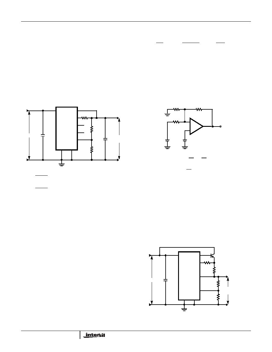
The circuit of Figure 8 illustrates proper use of the device.
CMOS devices generally require two precautions: every
input pin must go somewhere, and maximum values of
applied voltages and current limits must be rigorously
observed. Neglecting these precautions may lead to, at the
least, incorrect or nonoperation, and at worst, destructive
device failure. To avoid the problem of latchup, do not apply
inputs to any pins before supply voltage is applied.
Input Voltages - The ICL7663S accepts working inputs of
1.5V to 16V. When power is applied, the rate-of-rise of the
input may be hundreds of volts per microsecond. This is
potentially harmful to the regulators, where internal
operating currents are in the nanoampere range. The
0.047
µ
F capacitor on the device side of the switch will limit
inputs to a safe level around 2V/
µ
s. Use of this capacitor is
suggested in all applications. In severe rate-of-rise cases, it
may be advisable to use an RC network on the SHutDowN
pin to delay output turn-on. Battery charging surges,
transients, and assorted noise signals should be kept from
the regulators by RC filtering, zener protection, or even
fusing.
Output Voltages - The resistor divider R
2
/R
1
is used to
scale the reference voltage, V
SET
, to the desired output
using the formula V
OUT
= (1 + R
2
/R
1
) V
SET
. Suitable
arrangements of these resistors, using a potentiometer,
enables exact values for V
OUT
to be obtained. In most
applications the potentiometer may be eliminated by using
the ICL7663SA. The ICL7663SA has V
SET
voltage
guaranteed to be 1.29V
±
15mV and when used with
±
1%
tolerance resistors for R
1
and R
2
the initial output voltage
will be within
±
2.7% of ideal.
The low leakage current of the V
SET
terminal allows R
1
and
R
2
to be tens of megohms for minimum additional quiescent
drain current. However, some load current is required for
proper operation, so for extremely low-drain applications it is
necessary to draw at least 1
µ
A. This can include the current
for R
2
and R
1
.
Output voltages up to nearly the V
IN
supply may be obtained
at low load currents, while the low limit is the reference
voltage. The minimum input-output differential in each
regulator is obtained using the V
OUT1
, terminal. The input-
output differential increases to 1.5V when using V
OUT2
.
Output Currents - Low output currents of less than 5mA are
obtained with the least input-output differential from the
V
OUT1
terminal (connect V
OUT2
to V
OUT1
). Where higher
currents are needed, use V
OUT2
(V
OUT1
, should be left
open in this case).
SHDN
V
OUT2
V
OUT1
V
TC
V
SET
SENSE
GND
1
µ
A MIN
+
-
I
Q
S
2
S
1
R
CL
R
2
R
L
C
L
R
1
(7663 ONLY)
V
OUT
ON
OFF
S
3
1M
1.4V < V
SHDN
< V+
IN
0.047
µ
F
+
-
M
NOTES:
7. S
1
when closed disables output current limiting.
8. Close S
2
for V
OUT1
, open S
2
for V
OUT2
.
9. IQ quiescent currents measured at GND pin by meter M.
10. S
3
when ON, permits normal operation, when OFF, shuts down
both V
OUT1
and V
OUT2
.
FIGURE 7. ICL7663S TEST CIRCUIT
ICL7663S
60
High output currents can be obtained only as far as package
dissipation allows. It is strongly recommended that output
current-limit sensing be used in such cases.
Current-Limit Sensing - The on-chip comparator (C in the
Functional Diagram) permits shutdown of the regulator
output in the event of excessive current drain. As Figure 8
shows, a current-limiting resistor, R
CL
, is placed in series
with V
OUT2
and the SENSE terminal is connected to the
load side of R
CL
. When the current through R
CL
is high
enough to produce a voltage drop equal to V
CL
(0.5V) the
voltage feedback is by-passed and the regulator output will
be limited to this current. Therefore, when the maximum load
current (I
LOAD
) is determined, simply divide V
CL
by I
LOAD
to
obtain the value for R
CL
.
Logic-Controllable Shutdown - When equipment is not
needed continuously (e.g., in remote data-acquisition
systems), it is desirable to eliminate its drain on the system
until it is required. This usually means switches, with their
unreliable contacts. Instead, the ICL7663S can be shut
down by a logic signal, leaving only I
Q
(under 4
µ
A) as a
drain on the power source. Since this pin must not be left
open, it should be tied to ground if not needed. A voltage of
less than 0.3V for the ICL7663S will keep the regulator ON,
and a voltage level of more than 1.4V but less than V+
IN
will
turn the outputs OFF. If there is a possibility that the control
signal could exceed the regulator input (V+
IN
) the current
from this signal should be limited to 100
µ
A maximum by a
high value (1M
) series resistor. This situation may occur
when the logic signal originates from a system powered
separately from that of the regulator.
Additional Circuit Precautions - This regulator has poor
rejection of voltage fluctuations from AC sources above
10Hz or so. To prevent the output from responding (where
this might be a problem), a reservoir capacitor across the
load is advised. The value of this capacitor is chosen so that
the regulated output voltage reaches 90% of its final value in
20ms. From:
In addition, where such a capacitor is used, a current-limiting
resistor is also suggested (see "Current-Limit Sensing").
Producing Output Voltages with Negative Temperature
Coefficients -The ICL7663S has an additional output which
is 0.9V relative to GND and has a tempco of +2.5mV/
o
C. By
applying this voltage to the inverting input of amplifier A (i.e.,
the V
SET
pin), output voltages having negative TC may be
produced. The TC of the output voltage is controlled by the
R
2
/R
3
ratio (see Figure 9 and its design equations).
Applications
Boosting Output Current with External Transistor
The maximum available output current from the ICL7663S is
40mA. To obtain output currents greater than 40mA, an
external NPN transistor is used connected as shown in
Figure 10.
SHDN
V
OUT2
V
OUT1
V
TC
V
SET
SENSE
GND
R
2
C
L
V
IN
0.047
µ
F
V+
IN
604k
R
CL
20
210k
R
1
10
µ
F V
OUT
+5V
FIGURE 8. POSITIVE REGULATOR WITH CURRENT LIMIT
V
OUT
=
R
2
+ R
1
R
1
V
SET
= 5V
I
CL
=
V
CL
R
CL
= 25mA
I =
V
C ,C
t
=
I
OUT
(20 x 10
-3
)
0.9V
OUT
= 0.022
I
OUT
V
OUT
V
REF
V
SET
-
+
V
TC
-
+
R
1
R
2
V
OUT
R
3
-
+
Where:V
SET
= 1.3V
V
TC
= 0.9V
TCV
TC
= +2.5mV/
o
C
FIGURE 9. GENERATING NEGATIVE TEMPERATURE
COEFFICIENTS
EQ. 1: V
OUT
= V
SET
(
R
2
1 +
R
1
)
R
2
+
R
3
(V
SET
- V
TC
)
EQ. 2:
TC V
OUT
=
R
2
-
R
3
(TC V
TC
) in mV/
o
C
SHDN
V
OUT2
V
OUT1
V
SET
SENSE
GND
V
IN
10
µ
F
V+
IN
604k
100
210k
V
OUT
+5V
0.47
EXTERNAL PIN
POWER
TRANSISTOR
FIGURE 10. BOOSTING OUTPUT CURRENT WITH EXTERNAL
TRANSISTOR
ICL7663S

61
Generating a Temperature Compensated Display Drive Voltage
Temperature has an important effect in the variation of
threshold voltage in multiplexed LCD displays. As
temperature rises, the threshold voltage goes down. For
applications where the display temperature varies widely, a
temperature compensated display voltage, V
DISP
, can be
generated using the ICL7663S. This is shown in Figure 11
for the ICM7233 triplexed LCD display driver.
V
OUT2
V
OUT1
V
SET
GND
V+
IN
V
TC
V
DISP
ICM7233
ICL7663S
GND
DATA BUS
V+
+5V
1.8M
300k
2.7M
LOGIC
SYSTEM,
PROCESSOR,
ETC.
GND
FIGURE 11. GENERATING A MULTIPLEXED LCD DISPLAY DRIVE VOLTAGE
ICL7663S