3-62
TM
FN3182.4
ICL7665S
CMOS Micropower Over/Under Voltage
Detector
The ICL7665S Super CMOS Micropower Over/Under
Voltage Detector contains two low power, individually
programmable Voltage detectors on a single CMOS chip.
Requiring typically 3
µ
A for operation, the device is intended
for battery-operated systems and instruments which require
high or low voltage warnings, settable trip points, or fault
monitoring and correction. The trip points and hysteresis of
the two voltage detectors are individually programmed via
external resistors. An internal bandgap-type reference
provides an accurate threshold voltage while operating from
any supply in the 1.6V to 16V range.
The ICL7665S, Super Programmable Over/Under Voltage
Detector is a direct replacement for the industry standard
ICL7665B offering wider operating voltage and temperature
ranges, improved threshold accuracy (ICL7665SA), and
temperature coefficient, and guaranteed maximum supply
current. All improvements are highlighted in the electrical
characteristics section. All critical parameters are
guaranteed over the entire commercial and industrial
temperature ranges.
Features
∑ Guaranteed 10
µ
A Maximum Quiescent Current Over
Temperature
∑ Guaranteed Wider Operating Voltage Range Over Entire
Operating Temperature Range
∑ 2% Threshold Accuracy (ICL7665SA)
∑ Dual Comparator with Precision Internal Reference
∑ 100ppm/
o
C Temperature Coefficient of Threshold Voltage
∑ 100% Tested at 2V
∑ Output Current Sinking Ability . . . . . . . . . . . . Up to 20mA
∑ Individually Programmable Upper and Lower Trip Voltages
and Hysteresis Levels
Applications
∑ Pocket Pagers
∑ Portable Instrumentation
∑ Charging Systems
∑ Memory Power Back-Up
∑ Battery Operated Systems
∑ Portable Computers
∑ Level Detectors
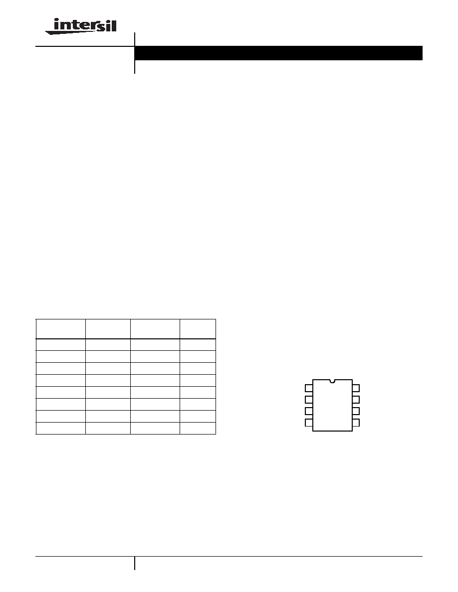
Pinout
ICL7665S
(SOIC, PDIP)
TOP VIEW
Ordering Information
PART NUMBER
TEMP. RANGE
(
o
C)
PACKAGE
PKG. NO.
ICL7665SCBA
0
to 70
8 Ld SOIC (N)
M8.15
ICL7665SCPA
0
to 70
8 Ld PDIP
E8.3
ICL7665SACBA
0
to 70
8 Ld SOIC (N)
M8.15
ICL7665SACPA
0
to 70
8 Ld PDIP
E8.3
ICL7665SIBA
-40
to 85
8 Ld SOIC (N)
M8.15
ICL7665SIPA
-40
to 85
8 Ld PDIP
E8.3
ICL7665SAIBA
-40
to 85
8 Ld SOIC (N)
M8.15
ICL7665SAIPA
-40
to 85
8 Ld PDIP
E8.3
OUT 1
HYST 1
SET 1
GND
1
2
3
4
8
7
6
5
V+
OUT 2
SET 2
HYST 2
Data Sheet
April 1999
CAUTION: These devices are sensitive to electrostatic discharge; follow proper IC Handling Procedures.
1-888-INTERSIL or 321-724-7143
|
Intersil (and design) is a trademark of Intersil Americas Inc.
Copyright © Intersil Americas Inc. 2002. All Rights Reserved

3-63
Absolute Maximum Ratings
Thermal Information
Supply Voltage (Note 2) . . . . . . . . . . . . . . . . . . . . . . . . . -0.3 to +18V
Output Voltages OUT1 and OUT2 . . . . . . . . . . . . . . . . . -0.3V to 18V
(with respect to GND) (Note 2)
Output Voltages HYST1 and HYST2 . . . . . . . . . . . . . . -0.3V to +18V
(with respect to V+) (Note 2)
Input Voltages SET1 and SET2 . . . . . (GND -0.3V) to (V+ V- +0.3V)
(Note 2)
Maximum Sink Output OUT1 and OUT2 . . . . . . . . . . . . . . . . . 25mA
Maximum Source Output Current
HYST1 and HYST2 . . . . . . . . . . . . . . . . . . . . . . . . . . . . . . -25mA
Operating Conditions
Temperature Range
ICL7665SC. . . . . . . . . . . . . . . . . . . . . . . . . . . . . . . . . 0
o
C to 70
o
C
ICL7665SI . . . . . . . . . . . . . . . . . . . . . . . . . . . . . . . -40
o
C to 85
o
C
Thermal Resistance (Typical, Note 1)
JA
(
o
C/W)
JC
(
o
C/W)
PDIP Package . . . . . . . . . . . . . . . . . . .
150
N/A
Plastic SOIC Package . . . . . . . . . . . . .
180
N/A
Maximum Junction Temperature (Plastic) . . . . . . . . . . . . . . . . 150
o
C
Maximum Junction Temperature (CERDIP). . . . . . . . . . . . . . . 175
o
C
Maximum Storage Temperature Range . . . . . . . . . . -65
o
C to 150
o
C
Maximum Lead Temperature (Soldering 10s) . . . . . . . . . . . . . 300
o
C
(SOIC - Lead Tips Only)
CAUTION: Stresses above those listed in "Absolute Maximum Ratings" may cause permanent damage to the device. This is a stress only rating and operation of the
device at these or any other conditions above those indicated in the operational sections of this specification is not implied.
NOTES:
1.
JA
is measured with the component mounted on an evaluation PC board in free air.
2. Due to the SCR structure inherent in the CMOS process used to fabricate these devices, connecting any terminal to voltages greater than (V+
+0.3V) or less than (GND - 0.3V) may cause destructive device latchup. For these reasons, it is recommended that no inputs from external
sources not operating from the same power supply be applied to the device before its supply is established, and that in multiple supply systems,
the supply to the ICL7665S be turned on first. If this is not possible, current into inputs and/or outputs must be limited to
±
0.5mA and voltages
must not exceed those defined above.
Electrical Specifications
The specifications below are applicable to both the ICL7665S and ICL7665SA. V+ = 5V, T
A
= 25
o
C,
Test Circuit Figure 7. Unless Otherwise Specified
PARAMETER
SYMBOL
TEST CONDITIONS
MIN
TYP
MAX
UNITS
Operating Supply Voltage
V+
ICL7665S
T
A
= 25
o
C
1.6
-
16
V
0
o
C
T
A
70
o
C
1.8
-
16
V
-25
o
C
T
A
85
o
C
1.8
-
16
V
ICL7665SA
0
o
C
T
A
70
o
C
1.8
-
16
V
-25
o
C
T
A
85
o
C
1.8
-
16
V
Supply Current
I+
GND
V
SET1
, V
SET2
V+, All Outputs Open Circuit
0
o
C
T
A
70
o
C
V+ = 2V
-
2.5
10
µ
A
V+ = 9V
-
2.6
10
µ
A
V+ = 15V
-
2.9
10
µ
A
-40
o
C
T
A
85
o
C
V+ = 2V
-
2.5
10
µ
A
V+ = 9V
-
2.6
10
µ
A
V+ = 15V
-
2.9
10
µ
A
Input Trip Voltage
V
SET1
ICL7665S
1.20
1.30
1.40
V
V
SET2
1.20
1.30
1.40
V
V
SET1
ICL7665SA
1.275
1.30
1.325
V
V
SET2
1.275
1.30
1.325
V
Temperature Coefficient of
V
SET
V
SET
T
ICL7665S
-
200
-
ppm
ICL7665SA
-
100
-
ppm
Supply Voltage Sensitivity of
V
SET1
, V
SET2
V
SET
V
S
R
OUT1
, R
OUT2
, R
HYST1
, R
2HYST2
= 1M
,
2V
V+
10V
-
0.03
-
%/V
ICL7665S
3-64
Output Leakage Currents of
OUT and HYST
I
OLK
V
SET
= 0V or V
SET
2V
-
10
200
nA
I
HLK
-
-10
-100
nA
I
OLK
V+ = 15V, T
A
= 70
o
C
-
-
2000
nA
I
HLK
-
-
-500
nA
Output Saturation Voltages
V
OUT1
V
SET1
= 2V,
I
OUT1
= 2mA
V+ = 2V
-
0.2
0.5
V
V+ = 5V
-
0.1
0.3
V
V+ = 15V
-
0.06
0.2
V
Output Saturation Voltages
V
HYST1
V
SET1
= 2V,
I
HYST1
= -0.5mA
V+ = 2V
-
-0.15
-0.30
V
V+ = 5V
-
-0.05
-0.15
V
V+ = 15V
-
-0.02
-0.10
V
Output Saturation Voltages
V
OUT2
V
SET2
= 0V,
I
OUT2
= 2mA
V+ = 2V
-
0.2
0.5
V
V+ = 5V
-
0.15
0.3
V
V+ = 15V
-
0.11
0.25
V
Output Saturation Voltages
V
HYST2
V
SET2
= 2V
V+ = 2V, I
HYST2
= -0.2mA
-
-0.25
-0.8
V
V+ = 5V, I
HYST2
= -0.5mA
-
-0.43
-1.0
V
V+ = 15V, I
HYST2
= -0.5mA
-
-0.35
-0.8
V
V
SET
Input Leakage Current
I
SET
GND
V
SET
V+
-
0.01
10
nA
Input for Complete Output
Change
V
SET
R
OUT
= 4.7k
,
R
HYST
= 20k
,
V
OUT
LO = 1% V+,
V
OUT
HI = 99% V+
ICL7665S
-
1.0
-
mV
ICL7665SA
-
0.1
-
mV
Difference in Trip Voltages
V
SET1
-
V
SET2
R
OUT
, R
HYST
= 1mW
-
±
5
±
50
mV
Output/Hysteresis
Difference
R
OUT
, R
HYST
= 1mW
ICL7665S
-
±
1
-
mV
ICL7665SA
-
±
0.1
-
mV
NOTES:
3. Derate above 25
o
C ambient temperature at 4mW/
o
C
4. All significant improvements over the industry standard ICL7665 are highlighted.
Electrical Specifications
The specifications below are applicable to both the ICL7665S and ICL7665SA. V+ = 5V, T
A
= 25
o
C,
Test Circuit Figure 7. Unless Otherwise Specified
(Continued)
PARAMETER
SYMBOL
TEST CONDITIONS
MIN
TYP
MAX
UNITS
AC Electrical Specifications
PARAMETER
SYMBOL
TEST CONDITIONS
MIN
TYP
MAX
UNITS
OUTPUT DELAY TIMES
Input Going HI
t
SO1D
V
SET
Switched between 1.0V to 1.6V
R
OUT
= 4.7k
, C
L
= 12pF
R
HYST
= 20k
, C
L
= 12pF
-
85
-
µ
s
t
SH1D
-
90
-
µ
s
t
SO2D
-
55
-
µ
s
t
SH2D
-
55
-
µ
s
Input Going LO
t
SO1D
V
SET
Switched between 1.6V to 1.0V
R
OUT
= 4.7k
, C
L
= 12pF
R
HYST
= 20k
, C
L
= 12pF
-
75
-
µ
s
t
SH1D
-
80
-
µ
s
t
SO2D
-
60
-
µ
s
t
SH2D
-
60
-
µ
s
ICL7665S
3-65
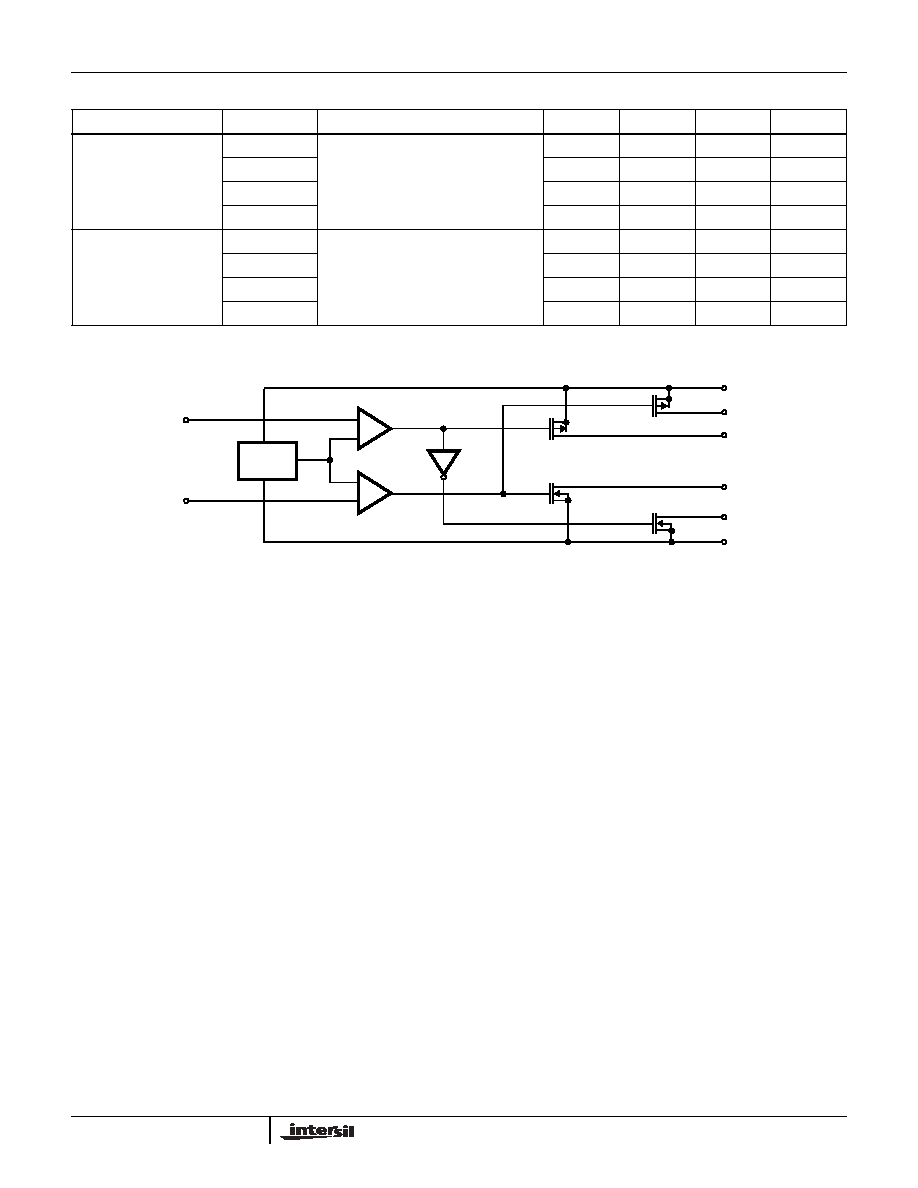
Functional Block Diagram
Output Rise Times
t
O1R
V
SET
Switched between 1.0V to 1.6V
R
OUT
= 4.7k
, C
L
= 12pF
R
HYST
= 20k
, C
L
= 12pF
-
0.6
-
µ
s
t
O2R
-
0.8
-
µ
s
t
H1R
-
7.5
-
µ
s
t
H2R
-
0.7
-
µ
s
Output Fall Times
t
O1F
V
SET
Switched between 1.0V to 1.6V
R
OUT
= 4.7k
, C
L
= 12pF
R
HYST
= 20k
, C
L
= 12pF
-
0.6
-
µ
s
t
O2F
-
0.7
-
µ
s
t
H1F
-
4.0
-
µ
s
t
H2F
-
1.8
-
µ
s
AC Electrical Specifications
(Continued)
PARAMETER
SYMBOL
TEST CONDITIONS
MIN
TYP
MAX
UNITS
REF
SET1
SET2
+
-
+
-
V+
HYST2
HYST1
OUT2
OUT1
GND
CONDITIONS (Note 5)
V
SET1
> 1.3V, OUT1 Switch ON, HYST1 Switch ON
V
SET1
< 1.3V, OUT1 Switch OFF, HYST1 Switch OFF
V
SET2
> 1.3V, OUT2 Switch OFF, HYST2 Switch ON
V
SET2
< 1.3V, OUT2 Switch ON, HYST2 Switch OFF
NOTE:
5. See Electrical Specifications for exact thresholds.
ICL7665S

3-66
Typical Performance Curves
FIGURE 1. OUT1 SATURATION VOLTAGE AS A FUNCTION
OF OUTPUT CURRENT
FIGURE 2. OUT2 SATURATION VOLTAGE AS A FUNCTION
OF OUTPUT CURRENT
FIGURE 3. HYST1 OUTPUT SATURATION VOLTAGE vs
HYST1 OUTPUT CURRENT
FIGURE 4. HYST2 OUTPUT SATURATION VOLTAGE vs
HYST2 OUTPUT CURRENT
FIGURE 5. SUPPLY CURRENT AS A FUNCTION OF AMBIENT
TEMPERATURE
FIGURE 6. SUPPLY CURRENT AS A FUNCTION OF SUPPLY
VOLTAGE
V
O
L
T
A
GE
S
A
T
U
R
A
T
I
ON
(
V
)
2.0
1.5
1.0
0.5
0
0
5
10
15
20
I
OUT
OUT1 (mA)
V+ = 2V
V+ = 5V
V+ = 15V
V+ = 9V
0
5
10
15
20
2.0
1.5
1.0
0.5
0
V
O
L
T
A
GE
S
A
T
U
R
A
T
I
ON
(
V
)
I
OUT
OUT2 (mA)
V+ = 2V
V+ = 5V
V+ = 9V
V+ = 15V
-20
-16
-12
-8
-4
0
0
-0.4
-0.8
-1.2
-1.6
-2.0
H
Y
S
T
1
O
U
T
P
UT
S
A
T
URA
T
I
O
N
V
O
L
T
AG
E
(
V
)
HYST1 OUTPUT CURRENT (mA)
V+ = 15V
V+ = 9V
V+ = 5V
V+ = 2V
T
A
= 25
o
C
-5.0
-4.0
-3.0
-2.0
-1.0
0
0
-1.0
-2.0
-3.0
-4.0
-5.0
HYST2 OUTPUT CURRENT (mA)
H
YST
2
O
U
T
P
U
T
S
A
T
U
R
A
T
I
O
N
VO
L
T
A
G
E
(
V
)
T
A
= 25
o
C
V+ = 15V
V+ = 9V
V+ = 5V
V+ = 2V
V+ = 2V
V+ = 15V
V+ = 9V
5.0
4.5
4.0
3.5
3.0
2.5
2.0
1.5
1.0
0.5
0
-25
0
+20
+40
+60
AMBIENT TEMPERATURE (
o
C)
S
U
P
P
L
Y
CURRE
NT
(
µ
A)
0V
V
SET1
, V
SET2
V+
0V
V
SET1
, V
SET2
V+
5.0
4.5
4.0
3.5
3.0
2.5
2.0
1.5
1.0
0.5
0
0
2
4
6
8
10
12
14
16
SUPPLY VOLTAGE (V+)
S
U
P
P
L
Y
CURRE
NT
(
µ
A)
T
A
= -20
o
C
T
A
= 25
o
C
T
A
= 70
o
C
ICL7665S
3-67
Detailed Description
As shown in the Functional Diagram, the ICL7665S consists
of two comparators which compare input voltages on the
SET1 and SET2 terminals to an internal 1.3V bandgap
reference. The outputs from the two comparators drive
open- drain N-channel transistors for OUT1 and OUT2, and
open- drain P-channel transistors for HYST1 and HYST2
outputs. Each section, the Under Voltage Detector and the
Over Voltage Detector, is independent of the other, although
both use the internal 1.3V reference. The offset voltages of
the two comparators will normally be unequal so V
SET1
will
generally not quite equal V
SET2
.
The input impedance of the SET1 and SET2 pins are
extremely high, and for most practical applications can be
ignored. The four outputs are open-drain MOS transistors,
and when ON behave as low resistance switches to their
respective supply rails. This minimizes errors in setting up
the hysteresis, and maximizes the output flexibility. The
operating currents of the bandgap reference and the
comparators are around 100nA each.
Precautions
Junction isolated CMOS devices like the ICL7665S have an
inherent SCR or 4-layer PNPN structure distributed
throughout the die. Under certain circumstances, this can be
triggered into a potentially destructive high current mode.
This latchup can be triggered by forward-biasing an input or
output with respect to the power supply, or by applying
excessive supply voltages. In very low current analog
circuits, such as the ICL7665S, this SCR can also be
triggered by applying the input power supply extremely
rapidly ("instantaneously"), e.g., through a low impedance
battery and an ON/OFF switch with short lead lengths. The
rate-of-rise of the supply voltage can exceed 100V/
µ
s in
such a circuit. A low impedance capacitor (e.g., 0.05
µ
F disc
ceramic) between the V+ and GND pins of the ICL7665S
can be used to reduce the rate-of-rise of the supply voltage
in battery applications. In line operated systems, the rate-of-
rise of the supply is limited by other considerations, and is
normally not a problem.
If the SET voltages must be applied before the supply
voltage V+, the input current should be limited to less than
0.5mA by appropriate external resistors, usually required for
voltage setting anyway. A similar precaution should be taken
with the outputs if it is likely that they will be driven by other
circuits to levels outside the supplies at any time.
Simple Threshold Detector
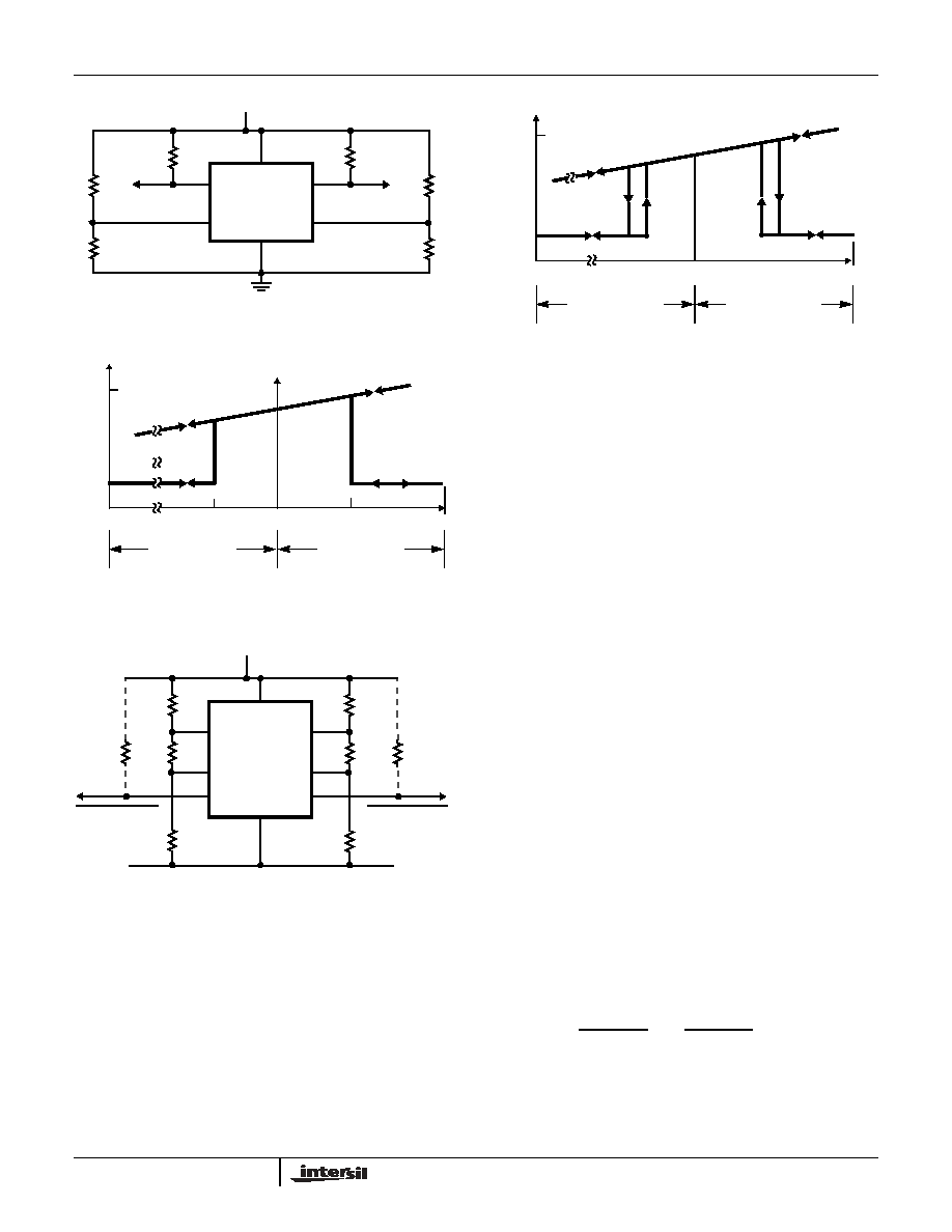
Figure 9 shows the simplest connection of the ICL7665S for
threshold detection. From the graph 9B, it can be seen that
at low input voltage OUT1 is OFF, or high, while OUT2 is
ON, or low. As the input rises (e.g., at power-on) toward
V
NOM
(usually the eventual operating voltage), OUT2 goes
high on reaching V
TR2
. If the voltage rises above V
NOM
as
much as V
TR1
, OUT1 goes low. The equation giving V
SET1
and V
SET2
are from Figure 9A:
Since the voltage to trip each comparator is nominally 1.3V,
the value V
IN
for each trip point can be found from
and
1
2
3
4
8
7
6
5
OUT1
HYST1
SET1
GND
V+
OUT2
SET2
HYST2
INPUT
HYST2
OUT2
OUT1
V+
20
k
12
pF
12
pF
12
pF
12
pF
20
k
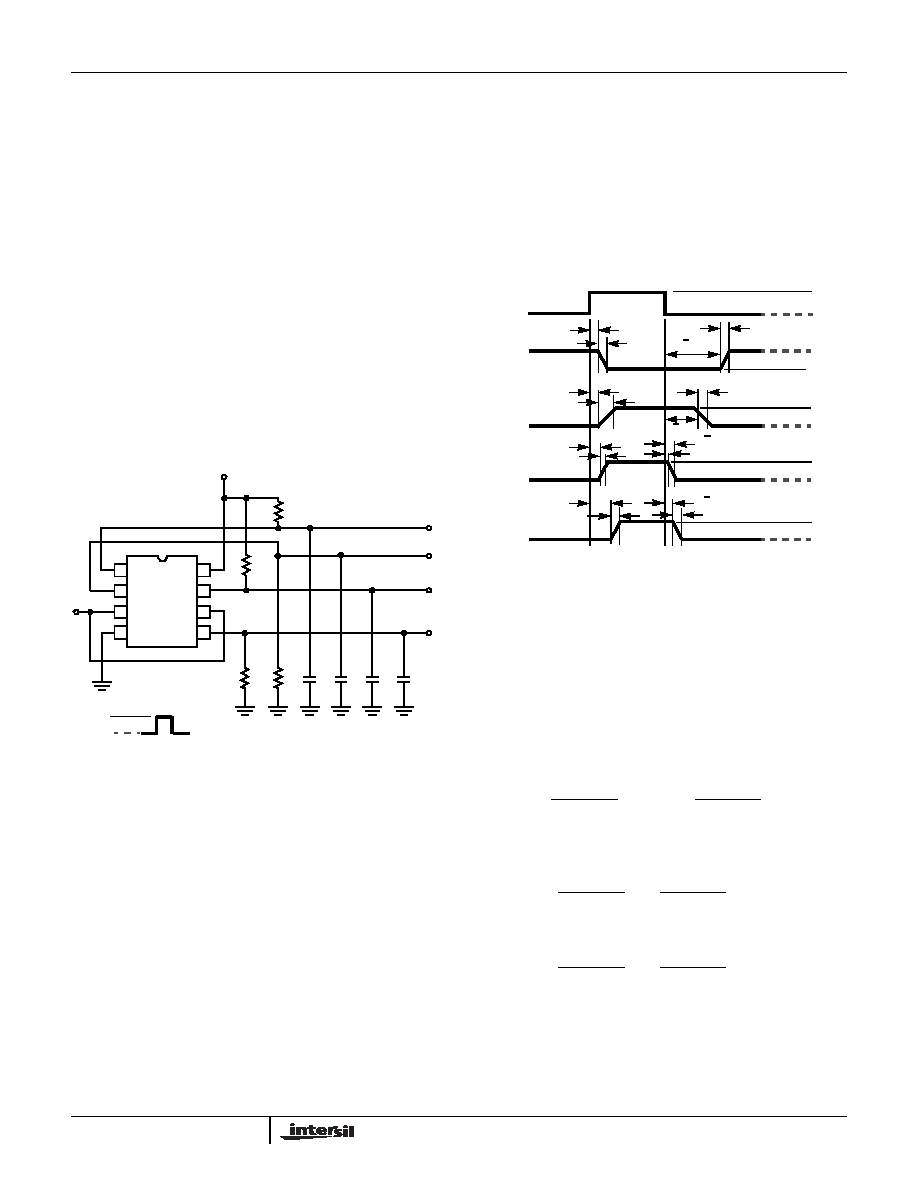
4.7k
HYST1
4.7
k
1.0V
1.6V
FIGURE 7. TEST CIRCUITS
V
SET1
=
V
IN
R
11
; V
SET2
=
V
IN
R
12
(R
11
+ R
21
)
(R
12
+ R
22
)
V
TR1
=
V
SET1
(R
11
+ R
21
)
= 1.3
(R
11
+ R
21
)
for detector 1
R
11
R
11
V
TR2
=
V
SET2
(R
12
+ R
22
)
= 1.3
(R
12
+ R
22
)
for detector 2
R
12
R
12
V
SET1
,
V
SET2
t
SO1D
t
O1F
t
SO1D
t
O1R
t
SH1D
t
H1R
t
SH1D
t
H1F
t
SO2D
t
O2R
t
SO2D
t
O2F
t
SH2
D
t
H2R
t
SH2D
t
H2F
1.6V
1.0V
V+
GND
GND
GND
GND
(5V)
V+
(5V)
V+
(5V)
V+
(5V)
INPUT
OUT1
HYST1
OUT2
HYST2
FIGURE 8. SWITCHING WAVEFORMS
ICL7665S
3-68
Either detector may be used alone, as well as both together,
in any of the circuits shown here.
When V
IN
is very close to one of the trip voltage, normal
variations and noise may cause it to wander back and forth
across this level, leading to erratic output ON and OFF
conditions. The addition of hysteresis, making the trip points
slightly different for rising and falling inputs, will avoid this
condition.
Threshold Detector with Hysteresis
Figure 10A shows how to set up such hysteresis, while
Figure 10B shows how the hysteresis around each trip point
produces switching action at different points depending on
whether V
IN
is rising or falling (the arrows indicated direction
of change. The HYST outputs are basically switches which
short out R
31
or R
32
when V
IN
is above the respective trip
point. Thus if the input voltage rises from a low value, the trip
point will be controlled by R
1N
, R
2N
, and R
3N
, until the trip
point is reached. As this value is passed, the detector
changes state, R
3N
is shorted out, and the trip point
becomes controlled by only R
1N
and R
2N
, a lower value.
The input will then have to fall to this new point to restore the
initial comparator state, but as soon as this occurs, the trip
point will be raised again.
An alternative circuit for obtaining hysteresis is shown in
Figure 11. In this configuration, the HYST pins put the extra
resistor in parallel with the upper setting resistor. The values
of the resistors differ, but the action is essentially the same.
The governing equations are given in Table 1. These ignore
the effects of the resistance of the HYST outputs, but these
can normally be neglected if the resistor values are above
about 100k
.
OUT1
SET1
SET2
OUT2
V+
R
21
R
P2
V
IN
R
P1
R
22
R
11
R
12
FIGURE 9A. CIRCUIT CONFIGURATION
OFF
V
OUT
ON
V
TR2
V
NOM
V
TR1
DETECTOR 2
DETECTOR 1
FIGURE 9B. TRANSFER CHARACTERISTICS
FIGURE 9. SIMPLE THRESHOLD DETECTOR
HYST1
SET1
SET2
HYST2
V+
V
IN
OUT1
OUT2
R
31
R
32
R
12
R
11
R
21
R
22
OVERVOLTAGE
OVERVOLTAGE
FIGURE 10A. CIRCUIT CONFIGURATION
V
TR2
=
V
SET2
(R
12
+ R
22
)
= 1.3
(R
12
+ R
22
)
for detector 2
R
12
R
12
V
L2
V
U2
V
L1
V
U1
ON
OUT
OFF
V
NOM
DETECTOR 2
DETECTOR 1
V
IN
FIGURE 10B. TRANSFER CHARACTERISTICS
FIGURE 10. THRESHOLD DETECTOR WITH HYSTERESIS
ICL7665S

3-69
Applications
Single Supply Fault Monitor
Figure 12 shows an over/under voltage fault monitor for a
single supply. The over voltage trip point is centered around
5.5V and the under voltage trip point is centered around
4.5V. Both have some hysteresis to prevent erratic output
ON and OFF conditions. The two outputs are connected in a
wired OR configuration with a pullup resistor to generate a
power OK signal.
Multiple Supply Fault Monitor
The ICL7665S can simultaneously monitor several supplies
when connected as shown in Figure 13. The resistors are
chosen such that the sum of the currents through R
21A
,
R
21B
, and R
31
is equal to the current through R
11
when the
two input voltage are at the desired low voltage detection
point. The current through R
11
at this point is equal to
1.3V/R
11
. The voltage at the V
SET
input depends on the
voltage of both supplies being monitored. The trip voltage of
one supply while the other supply is at the nominal voltage
will be different that the trip voltage when both supplies are
below their nominal voltages.
The other side of the ICL7665S can be used to detect the
absence of negative supplies. The trip points for OUT1
depend on both the negative supply voltages and the actual
voltage of the +5V supply.
TABLE 1. SET-POINT EQUATIONS
NO HYSTERESIS
Over-Voltage V
TRIP
=
R
11
+ R
21
R
11
x V
SET1
Over-Voltage V
TRIP
=
R
12
+ R
22
R
12
x V
SET2
HYSTERESIS PER FIGURE 10A
V
U1
=
R
11
+ R
21
+ R31
R
11
x V
SET1
Over-Voltage V
TRIP
V
L1
=
R
11
+ R
21
R
11
x V
SET1
V
U2
=
R
12
+ R
22
+ R
32
R
12
x V
SET2
Under-Voltage V
TRIP
V
L2
=
R
12
+ R
22
R
12
x V
SET2
HYSTERESIS PER FIGURE 11
V
U1
=
R
11
+ R
21
R
11
x V
SET1
Over-Voltage V
TRIP
V
L1
=
R
11
+
R
21
R
31
R
21
+
R
31
x V
SET1
R
11
V
U2
=
R
12
+ R
22
R
12
x V
SET2
Over-Voltage V
TRIP
V
L2
=
R
12
+
R
22
R
32
R
22
+ R
32
x V
SET2
R
12
OUT1
SET1
SET2
OUT2
V+
R
21
R
P
V
IN
R
P
R
22
R
11
R
12
HYST1
HYST2
R
31
R
32
FIGURE 11. AN ALTERNATIVE HYSTERESIS CIRCUIT
HYST1
V
SET1
V
SET2
HYST2
V+
OUT1
OUT2
324K
13M
5%
100K
249K
7.5M
5%
+5V SUPPLY
POWER
OK
100K
1M
V+
OPEN VOLTAGE
DETECTOR
V
U
= 5.55V
V
L
= 5.45V
OPEN VOLTAGE
DETECTOR
V
U
= 4.55V
V
L
= 4.45V
R
22
R
32
R
12
R
11
R
31
R
21
FIGURE 12. FAULT MONITOR FOR A SINGLE SUPPLY
ICL7665S

3-70
Combination Low Battery Warning and Low
Battery Disconnect
When using rechargeable batteries in a system, it is
important to keep the batteries from being overdischarged.
The circuit shown in Figure 14 provides a low battery
warning and also disconnects the low battery from the rest of
the system to prevent damage to the battery. OUT1 is used
to shutdown the ICL7663S when the battery voltage drops to
the value where the load should be disconnected. As long as
V
SET1
is greater than 1.3V, OUT1 is low, but when V
SET1
drops below 1.3V, OUT1 goes high shutting off the
ICL7663S. OUT2 is used for low battery warning. When
V
SET2
is greater than 1.3V, OUT2 is high and the low battery
warning is on. When V
SET2
drops below 1.3V, OUT2 is low
and the low battery warning goes off. The trip voltage for low
battery warning can be set higher than the trip voltage for
shutdown to give advance low battery warning before the
battery is disconnected.
Power Fail Warning and Powerup/Powerdown
Reset
Figure 15 shows a power fail warning circuit with
powerup/powerdown reset. When the unregulated DC input
is above the trip point, OUT1 is low. When the DC input
drops below the trip point, OUT1 shuts OFF and the power
fail warning goes high. The voltage on the input of the 7805
will continue to provide 5V out at 1A until V
IN
is less than
7.3V, this circuit will provide a certain amount of warning
before the 5V output begins to drop.
The ICL7665S OUT2 is used to prevent a microprocessor
from writing spurious data to a CMOS battery backup
memory by causing OUT2 to go low when the 7805 5V
output drops below the ICL7665S trip point.
FIGURE 13. MULTIPLE SUPPLY FAULT MONITOR
HYST1
V
SET1
V
SET2
HYST2
V+
OUT1
OUT2
274k
R
21
100k
22
POWER
OK
301
R
11
+5V
-15V
-5V
M
k
787
k
+5V
1
M
1.02M
R
21A
R
21B
22
M
49.9k
+5V
+15V
HYST1
SET1
SET2
HYST2
V+
OUT1
OUT2
R
31
R
32
R
12
R
11
R
21
R
22
GND
+
-
LOW BATTERY SHUTDOWN
1M
V+
OUT1
SHUTDOWN V
SET
OUT2
V+
GND
1M
LOW BATTERY WARNING
SENSE
100
+5V
1A
ICL7663S
ICL7665S
FIGURE 14. LOW BATTERY WARNING AND LOW BATTERY DISCONNECT
ICL7665S

3-71
Simple High/Low Temperature Alarm
Figure 16 illustrates a simple high/low temperature alarm
which uses the ICL7665S with an NPN transistor. The
voltage at the top of R
1
is determined by the V
BE
of the
transistor and the position of R
1
's wiper arm. This voltage
has a negative temperature coefficient. R
1
is adjusted so
that V
SET2
equals 1.3V when the NPN transistor's
temperature reaches the temperature selected for the high
temperature alarm. When this occurs, OUT2 goes low. R
2
is
adjusted so that V
SET1
equals 1.3V when the NPN
transistor's temperature reaches the temperature selected
for the low temperature alarm. When the temperature drops
below this limit, OUT1 goes low.
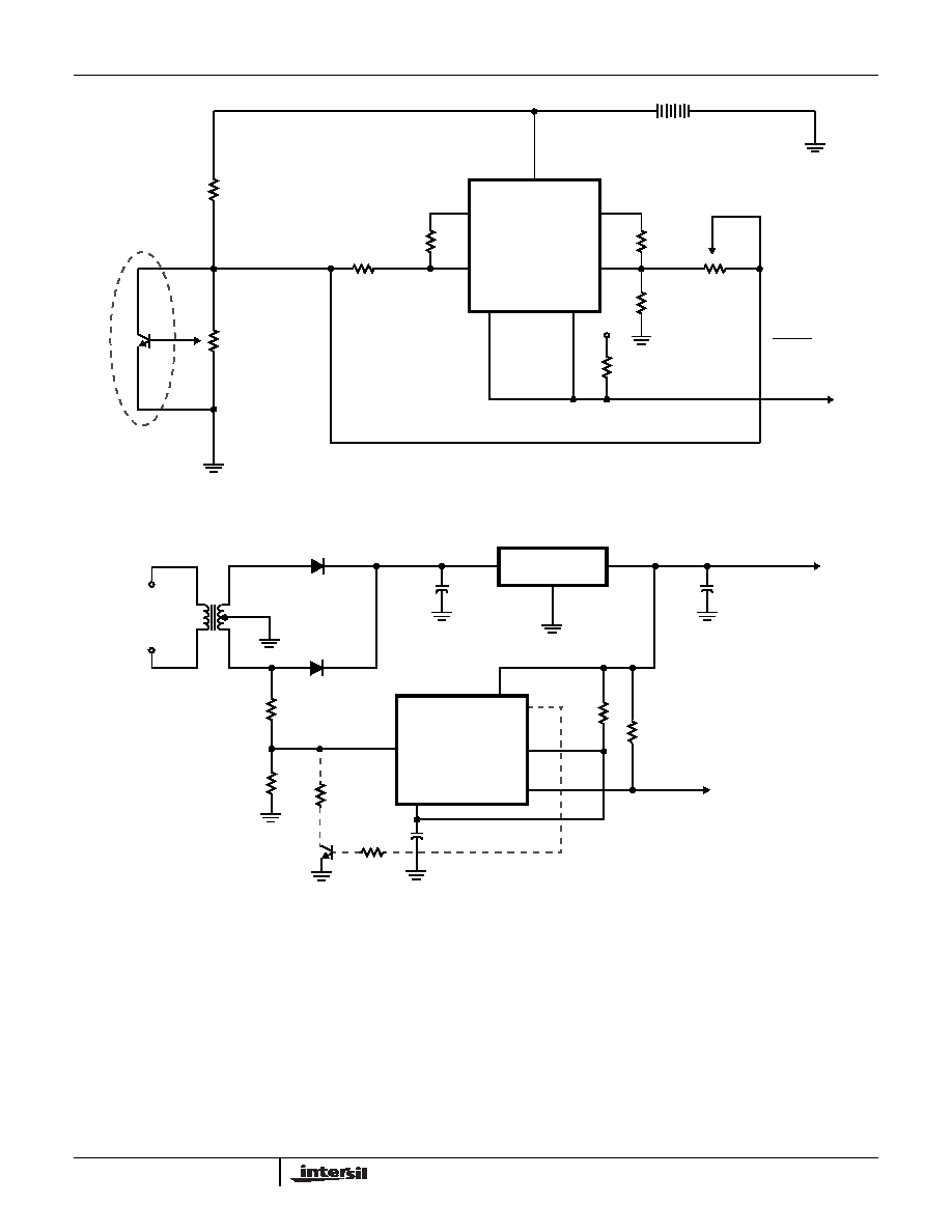
AC Power Fail and Brownout Detector
Figure 17 shows a circuit that detects AC undervoltage by
monitoring the secondary side of the transformer. The
capacitor, C
1
, is charged through R
1
when OUT1 is OFF.
With a normal 100 VAC input to the transformer, OUT1 will
discharge C
1
once every cycle, approximately every 16.7ms.
When the AC input voltage is reduced, OUT1 will stay OFF,
so that C
1
does not discharge. When the voltage on C
1
reaches 1.3V, OUT2 turns OFF and the power fail warning
goes high. The time constant, R
1
C
1
, is chosen such that it
takes longer than 16.7ms to charge C
1
1.3V.
HYST1
V
SET1
V
SET2
HYST2
V+
OUT1
OUT2
5.86k
130k
BACKUP
BATTERY
7805
5V REGULATOR
UNREGULATED
DC INPUT
1M
22M
2.2M
1M
715k
1M
RESET OR
WRITE
ENABLE
POWER
FAIL
WARNING
470
µ
F
4700
µ
F
ICL7665S
FIGURE 15. POWER FAIL WARNING AND POWERUP/POWERDOWN RESET
ICL7665S
3-72
HYST1
V
SET1
V
SET2
HYST2
V+
OUT1
OUT2
22k
1.5M
22M
1M
27k
R
4
R
5
V+
1M
R
7
R
2
R
6
ALARM SIGNAL
FOR DRIVING
LEDS, BELLS,
ETC.
LOW TEMPERATURE
LIMIT ADJUST
+
-
5V
470k
R
3
TEMPERATURE
SENSOR
(GENERAL PURPOSE
NPN TRANSISTOR)
10K
HIGH
TEMPERATURE
LIMIT ADJUST
R
1
ICL7665S
FIGURE 16. SIMPLE HIGH/LOW TEMPERATURE ALARM
110VAC
60Hz
20V
CENTERED
TAPPED
TRANS.
4700
µ
F
601k
100k
HYST1
V
SET1
V
SET2
HYST2
OUT1
OUT2
1M
1M
7805
5V REGULATOR
5V, 1A
C
1
R
1
1M
+5V
POWER FAIL
WARNING
ICL7665S
FIGURE 17. AC POWER FAIL AND BROWNOUT DETECTOR
ICL7665S