
3-81
TM
FN3183.2
ICL7673
Automatic Battery Back-Up Switch
The Intersil ICL7673 is a monolithic CMOS battery backup
circuit that offers unique performance advantages over
conventional means of switching to a backup supply. The
ICL7673 is intended as a low-cost solution for the switching
of systems between two power supplies; main and battery
backup. The main application is keep-alive-battery power
switching for use in volatile CMOS RAM memory systems
and real time clocks. In many applications this circuit will
represent a low insertion voltage loss between the supplies
and load. This circuit features low current consumption, wide
operating voltage range, and exceptionally low leakage
between inputs. Logic outputs are provided that can be used
to indicate which supply is connected and can also be used
to increase the power switching capability of the circuit by
driving external PNP transistors.
Pinouts
ICL7673 (SOIC, PDIP)
TOP VIEW
ICL7673 (CAN)
TOP VIEW
Features
∑ Automatically Connects Output to the Greater of Either
Input Supply Voltage
∑ If Main Power to External Equipment is Lost, Circuit Will
Automatically Connect Battery Backup
∑ Reconnects Main Power When Restored
∑ Logic Indicator Signaling Status of Main Power
∑ Low Impedance Connection Switches
∑ Low Internal Power Consumption
∑ Wide Supply Range: . . . . . . . . . . . . . . . . . . . 2.5V to 15V
∑ Low Leakage Between Inputs
∑ External Transistors May Be Added if Very Large
Currents Need to Be Switched
Applications
∑ On Board Battery Backup for Real-Time Clocks,
Timers, or Volatile RAMs
∑ Over/Under Voltage Detector
∑ Peak Voltage Detector
∑ Other Uses:
- Portable Instruments, Portable Telephones, Line
Operated Equipment
Functional Block Diagram
Ordering Information
PART
NUMBER
TEMP. RANGE
(
o
C)
PACKAGE
PKG. NO.
ICL7673CPA
0
to 70
8 Ld PDIP8
E8.3
ICL7673CBA
0
to 70
8 Ld SOIC (N)
M8.15
ICL7673ITV
25 to 85
8 Ld Metal Can T8.C
V
O
V
S
S
BAR
GDN
1
2
3
4
8
7
6
5
V
P
NC
P
BAR
NC
V
P
PBAR
V
S
V
O
SBAR
NC
NC
2
4
6
1
3
7
5
8
GND
P1
P2
V
S
GND
P
BAR
S
BAR
V
O
+
-
V
P
V
P
> V
S
, P1 SWITCH ON AND P
BAR
SWITCH ON
V
S
> V
P
, P2 SWITCH ON AND S
BAR
SWITCH ON
Data Sheet
April 1999
CAUTION: These devices are sensitive to electrostatic discharge; follow proper IC Handling Procedures.
1-888-INTERSIL or 321-724-7143
|
Intersil (and design) is a trademark of Intersil Americas Inc.
Copyright © Intersil Americas Inc. 2002. All Rights Reserved

3-82
Absolute Maximum Ratings
Thermal Information
Input Supply (V
P
or V
S
) Voltage . . . . . . . . . . . . GND - 0.3V to +18V
Output Voltages P
BAR
and S
BAR
. . . . . . . . . . . GND - 0.3V to +18V
Peak Current
Input V
P
(at V
P
= 5V) (Note 1) . . . . . . . . . . . . . . . . . . . . . . . 38mA
Input V
S
(at V
S
= 3V) . . . . . . . . . . . . . . . . . . . . . . . . . . . . . . 30mA
P
BAR
or S
BAR
. . . . . . . . . . . . . . . . . . . . . . . . . . . . . . . . . . 150mA
Operating Conditions
Temperature Range:
ICL7673C . . . . . . . . . . . . . . . . . . . . . . . . . . . . . . . . . . . 0
o
C to 70
o
C
ICL7673I. . . . . . . . . . . . . . . . . . . . . . . . . . . . . . . . . . -25
o
C to 85
o
C
Thermal Resistance (Typical, Note 2)
JA
(
o
C/W)
JC
(
o
C/W)
PDIP Package . . . . . . . . . . . . . . . . . . .
150
N/A
Plastic SOIC Package . . . . . . . . . . . . .
180
N/A
Metal Can. . . . . . . . . . . . . . . . . . . . . . .
156
68
o
C/W
Maximum Storage Temperature. . . . . . . . . . . . . . . . -65
o
C to 150
o
C
Maximum Lead Temperature (Soldering, 10sec). . . . . . . . . . . 300
o
C
(SOIC - Lead Tips Only)
CAUTION: Stresses above those listed in "Absolute Maximum Ratings" may cause permanent damage to the device. This is a stress only rating and operation of the
device at these or any other conditions above those indicated in the operational sections of this specification is not implied.
NOTES:
1. Derate above 25
o
C by 0.38mA/
o
C.
2.
JA
is measured with the component mounted on an evaluation PC board in free air.
Electrical Specifications
T
A
= 25
o
C Unless Otherwise Specified
PARAMETER
SYMBOL
TEST CONDITIONS
MIN
TYP
MAX
UNITS
Input Voltage
V
P
V
S
= 0V, I
LOAD
= 0mA
2.5
-
15
V
V
S
V
P
= 0V, I
LOAD
= 0mA
2.5
-
15
V
Quiescent Supply Current
I+
V
P
= 0V, V
S
= 3V, I
LOAD
= 0mA
-
1.5
5
µ
A
Switch Resistance P1 (Note 1)
r
DS(ON)
P1
V
P
= 5V, V
S
= 3V, I
LOAD
= 15mA
-
8
15
At T
A
= +85
o
C
-
16
-
V
P
= 9V, V
S
= 3V, I
LOAD
= 15mA
-
6
-
V
P
= 12V, V
S
= 3V, I
LOAD
= 15mA
-
5
-
Temperature Coefficient of Switch Re-
sistance P1
T
C(P1)
V
P
= 5V, V
S
= 3v, I
LOAD
= 15mA
-
0.5
-
%/
o
C
Switch Resistance P2 (Note 1)
r
DS(ON)
P2
V
P
= 0V, V
S
= 3V, I
LOAD
= 1mA
-
40
100
At T
A
= +85
o
C
-
60
-
V
P
= 0V, V
S
= 5V, I
LOAD
= 1mA
-
26
-
V
P
= 0V, V
S
= 9V, I
LOAD
= 1mA
-
16
-
Temperature Coefficient of Switch Re-
sistance P2
T
C(P2)
V
P
= 0V, V
S
= 3V, I
LOAD
= 1mA
-
0.7
-
%/
o
C
Leakage Current (V
P
to V
S
)
I
L(PS)
V
P
= 5V, V
S
= 3V, I
LOAD
= 10mA
-
0.01
20
nA
At T
A
= +85
o
C
-
35
-
nA
Leakage Current (V
P
to V
S
)
I
L(SP)
V
P
= 0V, V
S
= 3V, I
LOAD
= 10mA
-
0.01
50
nA
at T
A
= + 85
o
C
-
120
-
nA
Open Drain Output Saturation Voltages
V
OPBAR
V
P
= 5V, V
S
= 3V, I
SINK
= 3.2mA, I
LOAD
= 0mA
-
85
400
mV
At T
A
= 85
o
C
-
120
-
mV
V
P
= 9V, V
S
= 3V, I
SINK
= 3.2mA, I
LOAD
= 0mA
-
50
-
mV
V
P
= 12V, V
S
= 3V, I
SINK
= 3.2mA
I
LOAD
= 0mA
-
40
-
mV
ICL7673

3-83
Open Drain Output Saturation Voltages
V
OSBAR
V
P
= 0V, V
S
= 3V, I
SINK
= 3.2mA, I
LOAD
= 0mA
-
150
400
mV
at T
A
= + 85
o
C
-
210
-
mV
V
P
= 0V, V
S
= 5V, I
SINK
= 3.2mA I
LOAD
= 0mA
-
85
-
mV
V
P
= 0V, V
S
= 9V, I
SINK
= 3.2mA I
LOAD
= 0mA
-
50
-
mV
Output Leakage Currents of P
BAR
and
S
BAR
I
LPBAR
V
P
= 0V, V
S
= 15V, I
LOAD
= 0mA
-
50
500
nA
at T
A
= + 85
o
C
-
900
-
nA
I
LSBAR
V
P
= 15V, V
S
= 0V, I
LOAD
= 0mA
-
50
500
nA
at T
A
= + 85
o
C
-
900
-
nA
Switchover Uncertainty for Complete
Switching of Inputs and Open Drain
Outputs
V
P
- V
S
V
S
= 3V, I
SINK
= 3.2mA, I
LOAD
= 15mA
-
±
10
±
50
mV
NOTE:
3. The Minimum input to output voltage can be determined by multiplying the load current by the switch resistance.
Electrical Specifications
T
A
= 25
o
C Unless Otherwise Specified (Continued)
PARAMETER
SYMBOL
TEST CONDITIONS
MIN
TYP
MAX
UNITS
Typical Performance Curves
FIGURE 1. ON-RESISTANCE SWITCH P1 AS A FUNCTION OF
INPUT VOLTAGE V
P
FIGURE 2. ON-RESISTANCE SWITCH P2 AS A FUNCTION OF
INPUT VOLTAGE V
S
100
10
1
0
2
4
6
8
10
12
14
16
I
LOAD
= 15mA
O
N
-
R
E
S
IS
T
ANCE
P
1
(
)
INPUT VOLTAGE V
P
(V)
O
N
-
R
E
S
IS
T
ANCE
P
2
(
)
INPUT VOLTAGE V
S
100
10
1
0
2
4
6
8
10
I
LOAD
= 1mA
ICL7673

3-84
Detailed Description
As shown in the Functional Diagram, the ICL7673 includes a
comparator which senses the input voltages V
P
and V
S
. The
output of the comparator drives the first inverter and the
open-drain N-Channel transistor P
BAR
. The first inverter
drives a large P-Channel switch, P
1
, a second inverter, and
another open-drain N-Channel transistor, S
BAR
. The second
inverter drives another large P-Channel switch P
2
. The
ICL7673, connected to a main and a backup power supply,
will connect the supply of greater potential to its output. The
circuit provides break-before-make switch action as it
switches from main to backup power in the event of a main
power supply failure. For proper operation, inputs V
P
and V
S
must not be allowed to float, and, the difference in the two
supplies must be greater than 50mV. The leakage current
through the reverse biased parasitic diode of switch P
2
is
very low.
Output Voltage
The output operating voltage range is 2.5V to 15V. The
insertion loss between either input and the output is a
function of load current, input voltage, and temperature. This
is due to the P-Channels being operated in their triode
region, and, the ON-resistance of the switches is a function
of output voltage V
O
. The ON-resistance of the P-Channels
have positive temperature coefficients, and therefore as
temperature increases the insertion loss also increases. At
low load currents the output voltage is nearly equal to the
greater of the two inputs. The maximum voltage drop across
switch P
1
or P
2
is 0.5V, since above this voltage the body-
drain parasitic diode will become forward biased. Complete
switching of the inputs and open-drain outputs typically
occurs in 50
µ
s.
Input Voltage
The input operating voltage range for V
P
or V
S
is 2.5V to
15V. The input supply voltage (V
P
or V
S
) slew rate should be
limited to 2V per microsecond to avoid potential harm to the
circuit. In line-operated systems, the rate-of-rise (or fall) of
the supply is a function of power supply design. For battery
applications it may be necessary to use a capacitor between
the input and ground pins to limit the rate-of-rise of the
FIGURE 3. SUPPLY CURRENT AS A FUNCTION OF SUPPLY
VOLTAGE
FIGURE 4. P
BAR
OR S
BAR
SATURATION VOLTAGE AS A
FUNCTION OF OUTPUT CURRENT
Typical Performance Curves
(Continued)
S
U
P
P
L
Y
CURRE
NT
(
µ
A)
-40
o
C
25
o
C
85
o
C
1
0.8
0.6
0.4
0.2
0
2
4
6
8
10
12
14
16
SUPPLY VOLTAGE (V)
O
U
T
P
UT
S
A
T
URA
T
I
O
N
V
O
L
T
AG
E
(
V
)
5
4
3
2
1
0
40
80
120
140
180
V
O
= 3V
OUTPUT CURRENT (mA)
V
O
= 5V
V
O
= 9V
V
O
= 12V
V
O
= 15V
I
S
L
E
AKAG
E
CURRE
NT
INPUT V
P
(V)
0
2
4
5
6
8
10
12
1mA
100mA
10nA
1nA
1000pA
10pA
1pA
I
LOAD
= 10mA
V
S
= 0V
85
o
C
25
o
C
FIGURE 5. I
S
LEAKAGE CURRENT V
P
TO V
S
AS A
FUNCTION OF INPUT VOLTAGE
ICL7673

3-85
supply voltage. A low-impedance capacitor such as a
0.047
µ
F disc ceramic can be used to reduce the rate-of-rise.
Status Indicator Outputs
The N-Channel open drain output transistors can be used to
indicate which supply is connected, or can be used to drive
external PNP transistors to increase the power switching
capability of the circuit. When using external PNP power
transistors, the output current is limited by the beta and
thermal characteristics of the power transistors. The
application section details the use of external PNP
transistors.
Applications
A typical discrete battery backup circuit is illustrated in Figure
6. This approach requires several components, substantial
printed circuit board space, and high labor cost. It also
consumes a fairly high quiescent current. The ICL7673
battery backup circuit, illustrated in Figure 7, will often replace
such discrete designs and offer much better performance,
higher reliability, and lower system manufacturing cost. A
trickle charge system could be implemented with an additional
resistor and diode as shown in Figure 8. A complete low
power AC to regulated DC system can be implemented using
the ICL7673 and ICL7663S micropower voltage regulator as
shown in Figure 9.
Applications for the ICL7673 include volatile semiconductor
memory storage systems, real-time clocks, timers, alarm
systems, and over/under the voltage detectors. Other
systems requiring DC power when the master AC line supply
fails can also use the ICL7673.
A typical application, as illustrated in Figure 12, would be a
microprocessor system requiring a 5V supply. In the event of
primary supply failure, the system is powered down, and a
3V battery is employed to maintain clock or volatile memory
data. The main and backup supplies are connected to V
P
and V
S
, with the circuit output V
O
supplying power to the
clock or volatile memory. The ICL7673 will sense the main
supply, when energized, to be of greater potential than V
S
and connect, via its internal MOS switches, V
P
to output V
O
.
The backup input, V
S
will be disconnected internally. In the
event of main supply failure, the circuit will sense that the
backup supply is now the greater potential, disconnect V
P
from V
O
, and connect V
S
.
Figure 11 illustrates the use of external PNP power
transistors to increase the power switching capability of the
circuit. In this application the output current is limited by the
beta and thermal characteristics of the power transistors.
If hysteresis is desired for a particular low power application,
positive feedback can be applied between the input V
P
and
open drain output S
BAR
through a resistor as illustrated in
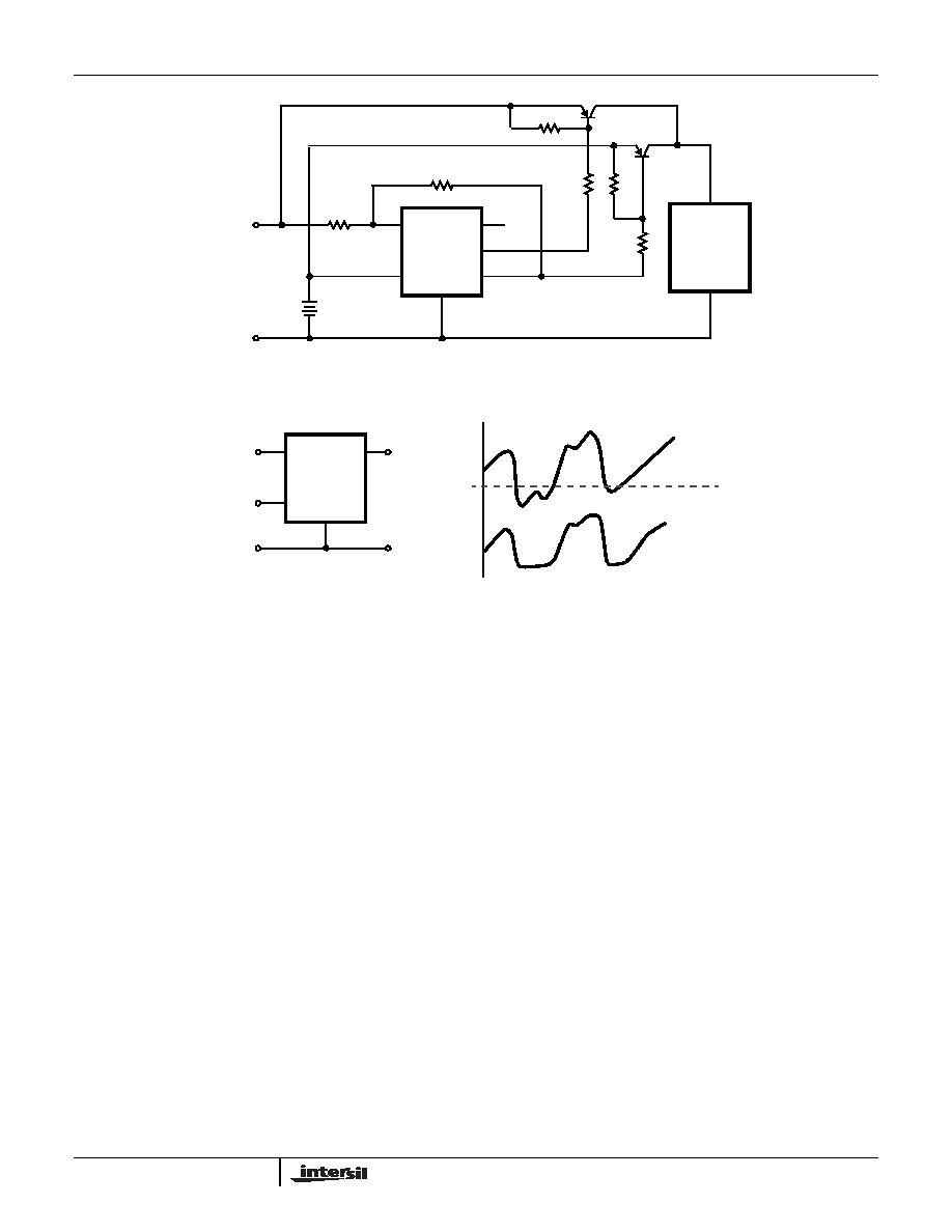
Figure 12. For high power applications hysteresis can be
applied as shown in Figure 13.
The ICL7673 can also be used as a clipping circuit as
illustrated in Figure 14. With high impedance loads the
circuit output will be nearly equal to the greater of the two
input signals.
+5V
PRIMARY
DC POWER
GND
NiCAD
BATTERY
STACK
V
O
+5V OR
+3V
STATUS
INDICATOR
FIGURE 6. DISCRETE BATTERY BACKUP CIRCUIT
V
P
V
O
V
S
GND
Pbar
8
2
1
6
V
O
+5V OR +3V
R
I
STATUS
INDICATOR
LITHIUM
BATTERY
GND
+5V
PRIMARY
SUPPLY
4
+
-
FIGURE 7. ICL7673 BATTERY BACKUP CIRCUIT
V
P
V
O
V
S
GND
8
2
1
V
O
+5V OR +3V
RECHARGEABLE
BATTERY
GND
+5V
PRIMARY
SUPPLY
4
R
C
+
-
FIGURE 8. APPLICATION REQUIRING RECHARGEABLE
BATTERY BACKUP
ICL7673

3-86
FIGURE 9. POWER SUPPLY FOR LOW POWER PORTABLE AC TO DC SYSTEMS
FIGURE 10. TYPICAL MICROPROCESSOR MEMORY APPLICATION
FIGURE 11. HIGH CURRENT BATTERY BACKUP SYSTEM
FIGURE 12. LOW CURRENT BATTERY BACKUP SYSTEM WITH HYSTERESIS
FUSE
120/240
VAC
BRIDGE
RECTIFIER
BATTERY
STACK
GND
V
O
V
S
V
P
1
8
2
4
2
8
4
6
STEPDOWN
TRANSFORMER
R
3
R
2
R
1
C
1
D
1
+
-
ICL7673
BATTERY
BACK-UP
ICL7663
REGULATOR
POWER
FAIL
DETECTOR
MICROPROCESSOR
VOLATILE
RAM
INTERRUPT SIGNAL
ICL7673
BACKUP CIRCUIT
+5V
MAIN
POWER
V
O
V
P
V
S
+
-
EXTERNAL
EQUIPMENT
V
O
GND
8
2
3
6
V
P
V
S
NC
P-
S-
1
PNP
PNP
MAIN
SUPPLY
3V
BACKUP
SUPPLY
+
-
(NOTE 4)
NOTE
4. > 1M
W
R
3
R
4
R
1
R
2
ICL7673
V
O
GND
8
2
3
V
P
V
S
S-
MAIN
SUPPLY
+
-
BATTERY
BACKUP
R
S
R
F
ICL7673
GND
GND
ICL7673
3-87
FIGURE 13. HIGH CURRENT BACKUP SYSTEM WITH HYSTERESIS
FIGURE 14. CLIPPLING CIRCUITS
EXTERNAL
EQUIPMENT
1
4
8
2
3
6
V
P
V
S
NC
P-
S-
PNP
PNP
MAIN
SUPPLY
BACKUP
SUPPLY
R
S
R
F
R
2
R
4
R
1
R
3
ICL7673
+V
SUPPLY
GND
MAIN
+
-
V
P
V
S
V
O
GND
V
S
V
O
V
P
ICL7673
ICL7673