1
CAUTION: These devices are sensitive to electrostatic discharge; follow proper IC Handling Procedures.
1-888-INTERSIL or 321-724-7143
|
Copyright
©
Intersil Corporation 1999
ICL8038
Precision Waveform Generator/Voltage
Controlled Oscillator
The ICL8038 waveform generator is a monolithic integrated
circuit capable of producing high accuracy sine, square,
triangular, sawtooth and pulse waveforms with a minimum of
external components. The frequency (or repetition rate) can
be selected externally from 0.001Hz to more than 300kHz
using either resistors or capacitors, and frequency
modulation and sweeping can be accomplished with an
external voltage. The ICL8038 is fabricated with advanced
monolithic technology, using Schottky barrier diodes and thin
film resistors, and the output is stable over a wide range of
temperature and supply variations. These devices may be
interfaced with phase locked loop circuitry to reduce
temperature drift to less than 250ppm/
o
C.
Features
∑ Low Frequency Drift with Temperature . . . . . . .250ppm/
o
C
∑ Low Distortion. . . . . . . . . . . . . . . . 1% (Sine Wave Output)
∑ High Linearity . . . . . . . . . . . 0.1% (Triangle Wave Output)
∑ Wide Frequency Range . . . . . . . . . . . 0.001Hz to 300kHz
∑ Variable Duty Cycle . . . . . . . . . . . . . . . . . . . . . 2% to 98%
∑ High Level Outputs . . . . . . . . . . . . . . . . . . . . . . TTL to 28V
∑ Simultaneous Sine, Square, and Triangle Wave
Outputs
∑ Easy to Use - Just a Handful of External Components
Required
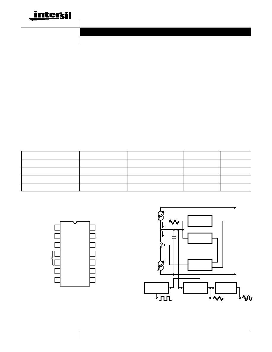
Pinout
ICL8038
(PDIP, CERDIP)
TOP VIEW
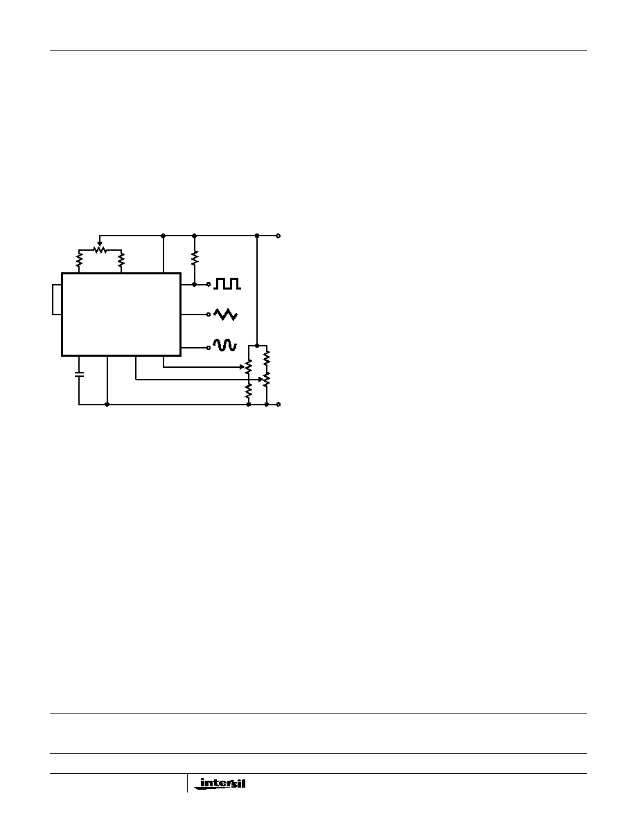
Functional Diagram
Ordering Information
PART NUMBER
STABILITY
TEMP. RANGE (
o
C)
PACKAGE
PKG. NO.
ICL8038CCPD
250ppm/
o
C (Typ)
0 to 70
14 Ld PDIP
E14.3
ICL8038CCJD
250ppm/
o
C (Typ)
0 to 70
14 Ld CERDIP
F14.3
ICL8038BCJD
180ppm/
o
C (Typ)
0 to 70
14 Ld CERDIP
F14.3
ICL8038ACJD
120ppm/
o
C (Typ)
0 to 70
14 Ld CERDIP
F14.3
SINE
TRIANGLE
DUTY CYCLE
V+
FM BIAS
NC
NC
SINE WAVE
V- OR GND
TIMING
SQUARE
FM SWEEP
1
2
3
4
5
6
7
14
13
12
11
10
9
8
ADJUST
CAPACITOR
WAVE OUT
INPUT
SINE WAVE
ADJUST
WAVE OUT
OUT
FREQUENCY
ADJUST
COMPARATOR
#1
COMPARATOR
#2
FLIP-FLOP
SINE
CONVERTER
BUFFER
BUFFER
9
2
11
I
10
6
V+
V- OR GND
CURRENT
SOURCE
#1
CURRENT
SOURCE
#2
2I
C
3
Data Sheet
September 1998
File Number
2864.3
2
Absolute Maximum Ratings
Thermal Information
Supply Voltage (V- to V+). . . . . . . . . . . . . . . . . . . . . . . . . . . . . . 36V
Input Voltage (Any Pin) . . . . . . . . . . . . . . . . . . . . . . . . . . . . V- to V+
Input Current (Pins 4 and 5). . . . . . . . . . . . . . . . . . . . . . . . . . . 25mA
Output Sink Current (Pins 3 and 9) . . . . . . . . . . . . . . . . . . . . . 25mA
Operating Conditions
Temperature Range
ICL8038AC, ICL8038BC, ICL8038CC . . . . . . . . . . . . 0
o
C to 70
o
C
Thermal Resistance (Typical, Note 1)
JA
(
o
C/W)
JC
(
o
C/W)
CERDIP Package . . . . . . . . . . . . . . . . .
75
20
PDIP Package . . . . . . . . . . . . . . . . . . .
115
N/A
Maximum Junction Temperature (Ceramic Package) . . . . . . . .175
o
C
Maximum Junction Temperature (Plastic Package) . . . . . . . .150
o
C
Maximum Storage Temperature Range . . . . . . . . . . -65
o
C to 150
o
C
Maximum Lead Temperature (Soldering 10s) . . . . . . . . . . . . 300
o
C
Die Characteristics
Back Side Potential . . . . . . . . . . . . . . . . . . . . . . . . . . . . . . . . . . . . V-
CAUTION: Stresses above those listed in "Absolute Maximum Ratings" may cause permanent damage to the device. This is a stress only rating and operation of the
device at these or any other conditions above those indicated in the operational sections of this specification is not implied.
NOTE:
1.
JA
is measured with the component mounted on an evaluation PC board in free air.
Electrical Specifications
V
SUPPLY
=
±
10V or +20V, T
A
= 25
o
C, R
L
= 10k
, Test Circuit Unless Otherwise Specified
PARAMETER
SYMBOL
TEST
CONDITIONS
ICL8038CC
ICL8038BC
ICL8038AC
UNITS
MIN
TYP
MAX
MIN
TYP
MAX
MIN
TYP
MAX
Supply Voltage Operating Range
V
SUPPLY
V+
Single Suppl
y
+10
-
+30
+10
-
+30
+10
-
+30
V
V+, V-
Dual Supplies
±
5
-
±
15
±
5
-
±
15
±
5
-
±
15
V
Supply Current
I
SUPPLY
V
SUPPLY
=
±
10V
(Note 2)
12
20
-
12
20
-
12
20
mA
FREQUENCY CHARACTERISTICS (All Waveforms)
Max. Frequency of Oscillation
f
MAX
100
-
-
100
-
-
100
-
-
kHz
Sweep Frequency of FM Input
f
SWEEP
-
10
-
-
10
-
-
10
-
kHz
Sweep FM Range
(Note 3)
-
35:1
-
-
35:1
-
-
35:1
-
FM Linearity
10:1 Ratio
-
0.5
-
-
0.2
-
-
0.2
-
%
Frequency Drift with
Temperature (Note 5)
f/
T
0
o
C to 70
o
C
-
250
-
-
180
-
-
120
ppm/
o
C
Frequency Drift with Supply Voltage
f/
V
Over Supply
Voltage Range
-
0.05
-
-
0.05
-
0.05
-
%/V
OUTPUT CHARACTERISTICS
Square Wave
Leakage Current
I
OLK
V
9
= 30V
-
-
1
-
-
1
-
-
1
µ
A
Saturation Voltage
V
SAT
I
SINK
= 2mA
-
0.2
0.5
-
0.2
0.4
-
0.2
0.4
V
Rise Time
t
R
R
L
= 4.7k
-
180
-
-
180
-
-
180
-
ns
Fall Time
t
F
R
L
= 4.7k
-
40
-
-
40
-
-
40
-
ns
Typical Duty Cycle Adjust
(Note 6)
D
2
98
2
-
98
2
-
98
%
Triangle/Sawtooth/Ramp
-
Amplitude
V
TRIAN-
GLE
R
TRI
= 100k
0.30
0.33
-
0.30
0.33
-
0.30
0.33
-
xV
SUPPLY
Linearity
-
0.1
-
-
0.05
-
-
0.05
-
%
Output Impedance
Z
OUT
I
OUT
= 5mA
-
200
-
-
200
-
-
200
-
ICL8038
3
Sine Wave
Amplitude
V
SINE
R
SINE
= 100k
0.2
0.22
-
0.2
0.22
-
0.2
0.22
-
xV
SUPPLY
THD
THD
R
S
= 1M
(Note 4)
-
2.0
5
-
1.5
3
-
1.0
1.5
%
THD Adjusted
THD
Use Figure 4
-
1.5
-
-
1.0
-
-
0.8
-
%
NOTES:
2. R
A
and R
B
currents not included.
3. V
SUPPLY
= 20V; R
A
and R
B
= 10k
, f
10kHz nominal; can be extended 1000 to 1. See Figures 5A and 5B.
4. 82k
connected between pins 11 and 12, Triangle Duty Cycle set at 50%. (Use R
A
and R
B
.)
5. Figure 1, pins 7 and 8 connected, V
SUPPLY
=
±
10V. See Typical Curves for T.C. vs V
SUPPLY
.
6. Not tested, typical value for design purposes only.
Electrical Specifications
V
SUPPLY
=
±
10V or +20V, T
A
= 25
o
C, R
L
= 10k
, Test Circuit Unless Otherwise Specified (Continued)
PARAMETER
SYMBOL
TEST
CONDITIONS
ICL8038CC
ICL8038BC
ICL8038AC
UNITS
MIN
TYP
MAX
MIN
TYP
MAX
MIN
TYP
MAX
Test Conditions
PARAMETER
R
A
R
B
R
L
C
SW
1
MEASURE
Supply Current
10k
10k
10k
3.3nF
Closed
Current Into Pin 6
Sweep FM Range (Note 7)
10k
10k
10k
3.3nF
Open
Frequency at Pin 9
Frequency Drift with Temperature
10k
10k
10k
3.3nF
Closed
Frequency at Pin 3
Frequency Drift with Supply Voltage (Note 8)
10k
10k
10k
3.3nF
Closed
Frequency at Pin 9
Output Amplitude (Note 10)
Sine
10k
10k
10k
3.3nF
Closed
Pk-Pk Output at Pin 2
Triangle
10k
10k
10k
3.3nF
Closed
Pk-Pk Output at Pin 3
Leakage Current (Off) (Note 9)
10k
10k
3.3nF
Closed
Current into Pin 9
Saturation Voltage (On) (Note 9)
10k
10k
3.3nF
Closed
Output (Low) at Pin 9
Rise and Fall Times (Note 11)
10k
10k
4.7k
3.3nF
Closed
Waveform at Pin 9
Duty Cycle Adjust (Note 11)
Max
50k
~1.6k
10k
3.3nF
Closed
Waveform at Pin 9
Min
~25k
50k
10k
3.3nF
Closed
Waveform at Pin 9
Triangle Waveform Linearity
10k
10k
10k
3.3nF
Closed
Waveform at Pin 3
Total Harmonic Distortion
10k
10k
10k
3.3nF
Closed
Waveform at Pin 2
NOTES:
7. The hi and lo frequencies can be obtained by connecting pin 8 to pin 7 (f
HI
) and then connecting pin 8 to pin 6 (f
LO
). Otherwise apply Sweep
Voltage at pin 8 (
2
/
3
V
SUPPLY
+2V)
V
SWEEP
V
SUPPLY
where V
SUPPLY
is the total supply voltage. In Figure 5B, pin 8 should vary between
5.3V and 10V with respect to ground.
8. 10V
V+
30V, or
±
5V
V
SUPPLY
±
15V.
9. Oscillation can be halted by forcing pin 10 to +5V or -5V.
10. Output Amplitude is tested under static conditions by forcing pin 10 to 5V then to -5V.
11. Not tested; for design purposes only.
ICL8038
4
Test Circuit
Application Information
(See Functional Diagram)
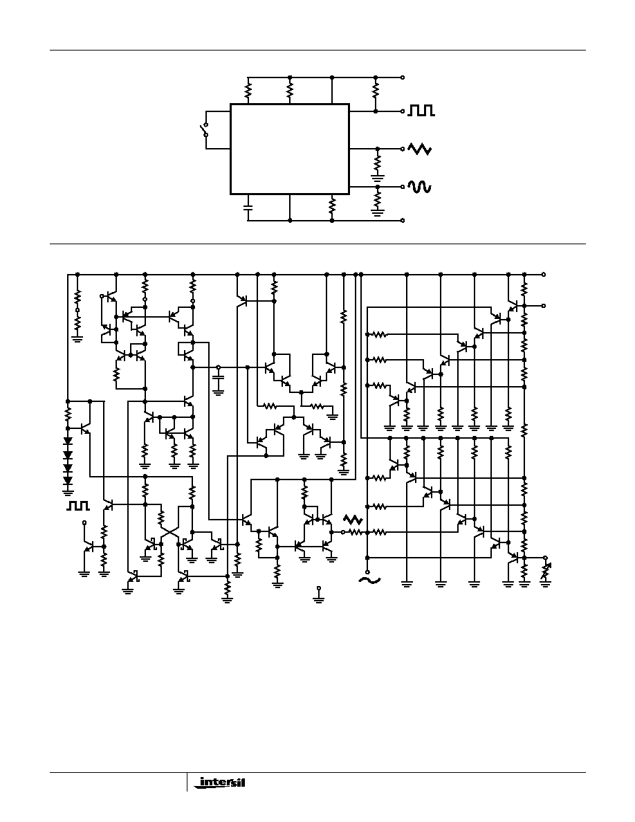
An external capacitor C is charged and discharged by two
current sources. Current source #2 is switched on and off by a
flip-flop, while current source #1 is on continuously. Assuming
that the flip-flop is in a state such that current source #2 is off,
and the capacitor is charged with a current I, the voltage
across the capacitor rises linearly with time. When this voltage
reaches the level of comparator #1 (set at 2/3 of the supply
voltage), the flip-flop is triggered, changes states, and
releases current source #2. This current source normally
carries a current 2I, thus the capacitor is discharged with a
net-current I and the voltage across it drops linearly with time.
When it has reached the level of comparator #2 (set at 1/3 of
the supply voltage), the flip-flop is triggered into its original
state and the cycle starts again.
Four waveforms are readily obtainable from this basic
generator circuit. With the current sources set at I and 2I
respectively, the charge and discharge times are equal. Thus
a triangle waveform is created across the capacitor and the
flip-flop produces a square wave. Both waveforms are fed to
buffer stages and are available at pins 3 and 9.
Detailed Schematic
ICL8038
4
5
6
9
2
12
11
10
8
7
SW
1
N.C.
C
3300pF
82K
R
A
10K
R
B
10K
R
L
10K
R
TRI
R
SINE
-10V
3
+10V
FIGURE 1. TEST CIRCUIT
Q
20
Q
21
Q
19
Q
22
Q
31
Q
32
Q
33
Q
34
Q
30
Q
7
Q
6
Q
1
Q
2
Q
4
Q
8
Q
9
Q
5
Q
3
Q
14
Q
11
Q
12
Q
13
Q
24
Q
23
Q
25
Q
26
Q
29
Q
27
Q
28
Q
10
Q
15
Q
18
Q
17
Q
16
Q
35
Q
36
Q
38
Q
40
Q
37
Q
39
R
1
11K
R
2
39K
7
8
5
4
R
EXT
B
R
EXT
A
COMPARATOR
R
41
4K
R
8
5K
R
9
5K
R
10
5K
R
43
27K
R
42
27K
BUFFER AMPLIFIER
R
41
27K
R
17
4.7K
R
18
4.7K
R
14
27K
R
13
620
R
16
1.8K
R
6
100
R
5
100
R
4
100
R
3
30K
R
46
40K
C
EXT
R
7A
10K
R
7B
15K
R
44
1K
3
10
R
11
270
R
12
2.7K
R
15
470
R
24
800
2
R
21
10K
R
20
2.7K
R
19
800
FLIP-FLOP
SINE CONVERTER
Q
49
Q
50
Q
52
Q
51
Q
53
Q
55
Q
54
Q
56
Q
42
Q
41
Q
43
Q
44
Q
45
Q
46
Q
47
Q
48
6
V+
1
12
R
32
5.2K
R
33
200
R
34
375
R
35
330
R
36
1600
R
37
330
R
38
375
R
39
200
R
40
5.6K
R
EXT
C
82K
R
23
2.7K
R
22
10K
R
28
33K
R
30
33K
R
29
33K
R
31
33K
R
25
33K
R
26
33K
R
27
33K
R
45
33K
CURRENT SOURCES
9
11
ICL8038

5
The levels of the current sources can, however, be selected
over a wide range with two external resistors. Therefore, with
the two currents set at values different from I and 2I, an
asymmetrical sawtooth appears at Terminal 3 and pulses
with a duty cycle from less than 1% to greater than 99% are
available at Terminal 9.
The sine wave is created by feeding the triangle wave into a
nonlinear network (sine converter). This network provides a
decreasing shunt impedance as the potential of the triangle
moves toward the two extremes.
Waveform Timing
The symmetry of all waveforms can be adjusted with the
external timing resistors. Two possible ways to accomplish
this are shown in Figure 3. Best results are obtained by
keeping the timing resistors R
A
and R
B
separate (A). R
A
controls the rising portion of the triangle and sine wave and
the 1 state of the square wave.
The magnitude of the triangle waveform is set at
1
/
3
V
SUPPLY
; therefore the rising portion of the triangle is,
The falling portion of the triangle and sine wave and the 0
state of the square wave is:
Thus a 50% duty cycle is achieved when R
A
= R
B
.
If the duty cycle is to be varied over a small range about 50%
only, the connection shown in Figure 3B is slightly more
convenient. A 1k
potentiometer may not allow the duty cycle
to be adjusted through 50% on all devices. If a 50% duty cycle
is required, a 2k
or 5k
potentiometer should be used.
With two separate timing resistors, the frequency is given by:
or, if R
A
= R
B
= R
t
1
C
V
◊
I
--------------
C
1/3
V
SUPPLY
R
A
◊
◊
◊
0.22
V
SUPPLY
◊
-------------------------------------------------------------------
R
A
C
◊
0.66
------------------
=
=
=
t
2
C
V
◊
1
-------------
C
1 /3 V
SUPPLY
◊
2 0.22
(
)
V
SUPPLY
R
B
------------------------
0.22
V
SUPPLY
R
A
------------------------
≠
-----------------------------------------------------------------------------------
R
A
R
B
C
0.66 2 RA RB
≠
(
)
--------------------------------------
=
=
=
f
1
t
1
t
2
+
----------------
1
R
A
C
0.66
------------
1
R
B
2R
A
R
B
≠
-------------------------
+
------------------------------------------------------
=
=
f
0.33
RC
-----------
(for Figure 3A)
=
FIGURE 2A. SQUARE WAVE DUTY CYCLE - 50%
FIGURE 2B. SQUARE WAVE DUTY CYCLE - 80%
FIGURE 2. PHASE RELATIONSHIP OF WAVEFORMS
FIGURE 3A.
FIGURE 3B.
FIGURE 3. POSSIBLE CONNECTIONS FOR THE EXTERNAL TIMING RESISTORS
C
82K
ICL8038
4
5
6
9
2
12
11
10
8
7
R
A
R
L
V- OR GND
3
R
B
V+
ICL8038
4
5
6
9
2
12
11
10
8
7
C
100K
R
A
R
L
V- OR GND
3
R
B
V+
1k
ICL8038
6
All Intersil semiconductor products are manufactured, assembled and tested under ISO9000 quality systems certification.
Intersil semiconductor products are sold by description only. Intersil Corporation reserves the right to make changes in circuit design and/or specifications at any time with-
out notice. Accordingly, the reader is cautioned to verify that data sheets are current before placing orders. Information furnished by Intersil is believed to be accurate and
reliable. However, no responsibility is assumed by Intersil or its subsidiaries for its use; nor for any infringements of patents or other rights of third parties which may result
from its use. No license is granted by implication or otherwise under any patent or patent rights of Intersil or its subsidiaries.
For information regarding Intersil Corporation and its products, see web site http://www.intersil.com
Neither time nor frequency are dependent on supply voltage,
even though none of the voltages are regulated inside the
integrated circuit. This is due to the fact that both currents
and thresholds are direct, linear functions of the supply
voltage and thus their effects cancel.
Reducing Distortion
To minimize sine wave distortion the 82k
resistor between
pins 11 and 12 is best made variable. With this arrangement
distortion of less than 1% is achievable. To reduce this even
further, two potentiometers can be connected as shown in
Figure 4; this configuration allows a typical reduction of sine
wave distortion close to 0.5%.
Selecting R
A
, R
B
and C
For any given output frequency, there is a wide range of RC
combinations that will work, however certain constraints are
placed upon the magnitude of the charging current for
optimum performance. At the low end, currents of less than
1
µ
A are undesirable because circuit leakages will contribute
significant errors at high temperatures. At higher currents
(I > 5mA), transistor betas and saturation voltages will
contribute increasingly larger errors. Optimum performance
will, therefore, be obtained with charging currents of 10
µ
A to
1mA. If pins 7 and 8 are shorted together, the magnitude of
the charging current due to R
A
can be calculated from:
R
1
and R
2
are shown in the Detailed Schematic.
A similar calculation holds for R
B
.
The capacitor value should be chosen at the upper end of its
possible range.
Waveform Out Level Control and Power Supplies
The waveform generator can be operated either from a
single power supply (10V to 30V) or a dual power supply
(
±
5V to
±
15V). With a single power supply the average levels
of the triangle and sine wave are at exactly one-half of the
supply voltage, while the square wave alternates between
V+ and ground. A split power supply has the advantage that
all waveforms move symmetrically about ground.
The square wave output is not committed. A load resistor
can be connected to a different power supply, as long as the
applied voltage remains within the breakdown capability of
the waveform generator (30V). In this way, the square wave
output can be made TTL compatible (load resistor
connected to +5V) while the waveform generator itself is
powered from a much higher voltage.
Frequency Modulation and Sweeping
The frequency of the waveform generator is a direct function
of the DC voltage at Terminal 8 (measured from V+). By
altering this voltage, frequency modulation is performed. For
small deviations (e.g.
±
10%) the modulating signal can be
applied directly to pin 8, merely providing DC decoupling
with a capacitor as shown in Figure 5A. An external resistor
between pins 7 and 8 is not necessary, but it can be used to
increase input impedance from about 8k
(pins 7 and 8
connected together), to about (R + 8k
).
For larger FM deviations or for frequency sweeping, the
modulating signal is applied between the positive supply
voltage and pin 8 (Figure 5B). In this way the entire bias for
the current sources is created by the modulating signal, and
a very large (e.g. 1000:1) sweep range is created (f = 0 at
V
SWEEP
= 0). Care must be taken, however, to regulate the
supply voltage; in this configuration the charge current is no
longer a function of the supply voltage (yet the trigger
thresholds still are) and thus the frequency becomes
dependent on the supply voltage. The potential on Pin 8 may
be swept down from V+ by (
1
/
3
V
SUPPLY
- 2V).
ICL8038
4
5
6
9
2
12
11
10
8
7
C
100k
R
A
R
L
V- OR GND
3
R
B
V+
1k
1
10k
100k
10k
FIGURE 4. CONNECTION TO ACHIEVE MINIMUM SINE WAVE
DISTORTION
I
R
1
V+
V-
≠
(
)
◊
R
1
R
2
+
(
)
----------------------------------------
1
R
A
--------
◊
0.22 V+
V-
≠
(
)
R
A
------------------------------------
=
=
ICL8038
7
Typical Applications
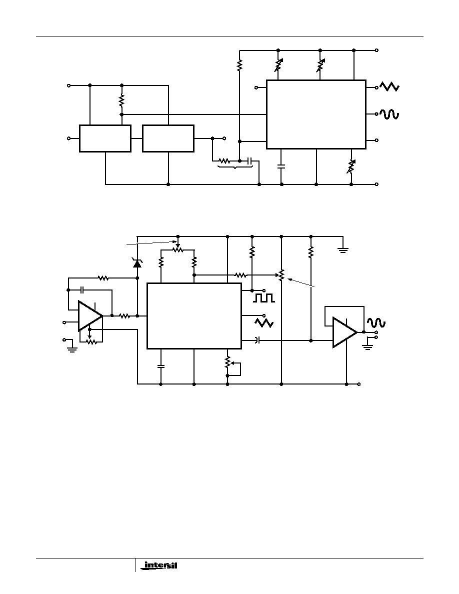
The sine wave output has a relatively high output impedance
(1k
Typ). The circuit of Figure 6 provides buffering, gain
and amplitude adjustment. A simple op amp follower could
also be used.
With a dual supply voltage the external capacitor on Pin 10 can
be shorted to ground to halt the ICL8038 oscillation. Figure 7
shows a FET switch, diode ANDed with an input strobe signal
to allow the output to always start on the same slope.
To obtain a 1000:1 Sweep Range on the ICL8038 the
voltage across external resistors R
A
and R
B
must decrease
to nearly zero. This requires that the highest voltage on
control Pin 8 exceed the voltage at the top of R
A
and R
B
by a
few hundred mV. The Circuit of Figure 8 achieves this by
using a diode to lower the effective supply voltage on the
ICL8038. The large resistor on pin 5 helps reduce duty cycle
variations with sweep.
The linearity of input sweep voltage versus output frequency
can be significantly improved by using an op amp as shown
in Figure 10.
C
81K
ICL8038
4
5
6
9
2
12
11
10
8
7
R
A
R
L
V- OR GND
3
R
B
V+
R
FM
FIGURE 5A. CONNECTIONS FOR FREQUENCY MODULATION
C
81K
ICL8038
4
5
6
9
2
12
11
10
8
R
A
R
L
V- OR GND
3
R
B
V+
SWEEP
VOLTAGE
FIGURE 5B. CONNECTIONS FOR FREQUENCY SWEEP
FIGURE 5.
C
ICL8038
4
5
6
2
11
10
8
7
R
A
100K
V-
R
B
V+
AMPLITUDE
20K
+
-
741
4.7K
FIGURE 6. SINE WAVE OUTPUT BUFFER AMPLIFIERS
C
ICL8038
4
5
9
10
11
8
7
R
A
1N914
-15V
R
B
V+
STROBE
2
2N4392
1N914
15K
100K
OFF
ON
+15V (+10V)
-15V (-10V)
FIGURE 7. STROBE TONE BURST GENERATOR
0.0047
µ
F
DISTORTION
ICL8038
5
4
6
9
2
12
11
10
8
4.7K
-10V
3
+10V
20K
4.7K
1K
DUTY CYCLE
15K
1N457
0.1
µ
F
100K
15M
10K
FREQ.
FIGURE 8. VARIABLE AUDIO OSCILLATOR, 20Hz TO 20kHzY
ICL8038
8
Use in Phase Locked Loops
Its high frequency stability makes the ICL8038 an ideal
building block for a phase locked loop as shown in Figure 9.
In this application the remaining functional blocks, the phase
detector and the amplifier, can be formed by a number of
available ICs (e.g., MC4344, NE562).
In order to match these building blocks to each other, two
steps must be taken. First, two different supply voltages are
used and the square wave output is returned to the supply of
the phase detector. This assures that the VCO input voltage
will not exceed the capabilities of the phase detector. If a
smaller VCO signal is required, a simple resistive voltage
divider is connected between pin 9 of the waveform
generator and the VCO input of the phase detector.
Second, the DC output level of the amplifier must be made
compatible to the DC level required at the FM input of the
waveform generator (pin 8, 0.8V+). The simplest solution here
is to provide a voltage divider to V+ (R
1
, R
2
as shown) if the
amplifier has a lower output level, or to ground if its level is
higher. The divider can be made part of the low-pass filter.
This application not only provides for a free-running
frequency with very low temperature drift, but is also has the
unique feature of producing a large reconstituted sinewave
signal with a frequency identical to that at the input.
For further information, see Intersil Application Note AN013,
"Everything You Always Wanted to Know About the ICL8038".
SINE WAVE
ICL8038
4
5
6
3
1
12
11
10
8
7
R
1
V-/GND
2
DUTY
V
2
+
CYCLE
FREQUENCY
ADJUST
ADJ.
9
SINE WAVE
TRIANGLE
OUT
SINE WAVE
ADJ.
TIMING
CAP.
FM BIAS
SQUARE
WAVE
OUT
R
2
LOW PASS
FILTER
DEMODULATED
FM
AMPLIFIER
PHASE
DETECTOR
VCO
IN
INPUT
V
1
+
OUT
FIGURE 9. WAVEFORM GENERATOR USED AS STABLE VCO IN A PHASE-LOCKED LOOP
3,900pF
SINE WAVE
ICL8038
4
5
6
9
2
12
11
10
8
4.7k
3
4.7k
500
10k
1N753A
DISTORTION
FUNCTION GENERATOR
100k
+
50
µ
F
15V
1M
(6.2V)
HIGH FREQUENCY
SYMMETRY
100k
LOW FREQUENCY
SYMMETRY
100k
+
-
741
+15V
-15V
SINE WAVE
OUTPUT
+
-
741
+15V
1k
10k
OFFSET
-V
IN
P
4
1,000pF
1k
FIGURE 10. LINEAR VOLTAGE CONTROLLED OSCILLATOR
ICL8038
9
Definition of Terms
Supply Voltage (V
SUPPLY
). The total supply voltage from
V+ to V-.
Supply Current. The supply current required from the
power supply to operate the device, excluding load currents
and the currents through R
A
and R
B
.
Frequency Range. The frequency range at the square wave
output through which circuit operation is guaranteed.
Sweep FM Range. The ratio of maximum frequency to
minimum frequency which can be obtained by applying a
sweep voltage to pin 8. For correct operation, the sweep
voltage should be within the range:
(
2
/
3
V
SUPPLY
+ 2V) < V
SWEEP
< V
SUPPLY
FM Linearity. The percentage deviation from the best fit
straight line on the control voltage versus output frequency
curve.
Output Amplitude. The peak-to-peak signal amplitude
appearing at the outputs.
Saturation Voltage. The output voltage at the collector of
Q
23
when this transistor is turned on. It is measured for a
sink current of 2mA.
Rise and Fall Times. The time required for the square wave
output to change from 10% to 90%, or 90% to 10%, of its
final value.
Triangle Waveform Linearity. The percentage deviation
from the best fit straight line on the rising and falling triangle
waveform.
Total Harmonic Distortion. The total harmonic distortion at
the sine wave output.
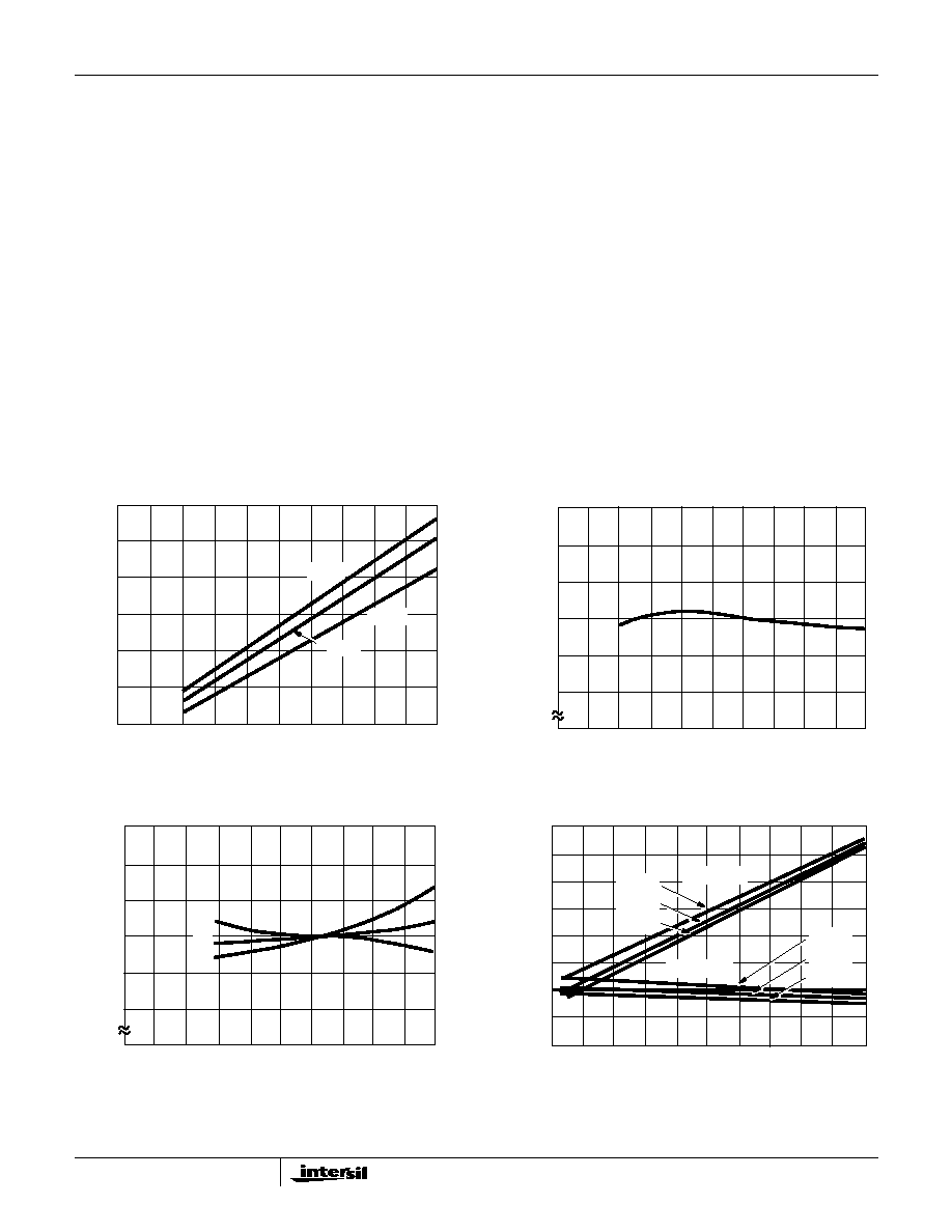
Typical Performance Curves
FIGURE 11. SUPPLY CURRENT vs SUPPLY VOLTAGE
FIGURE 12. FREQUENCY vs SUPPLY VOLTAGE
FIGURE 13. FREQUENCY vs TEMPERATURE
FIGURE 14. SQUARE WAVE OUTPUT RISE/FALL TIME vs
LOAD RESISTANCE
SUPPLY VOLTAGE (V)
SUPPL
Y CURRENT (mA)
5
10
15
20
25
30
5
10
15
20
25
o
C
125
o
C
-55
o
C
SUPPLY VOLTAGE (V)
NORMALIZED FREQ
UENCY
5
10
15
20
25
30
0.98
0.99
1.01
1.03
1.00
1.02
TEMPERATURE (
o
C)
NORMALIZED FREQ
UENCY
-50
-25
0
25
75
125
0.98
0.99
1.01
1.03
1.00
1.02
30
20
10
20
30
10
LOAD RESISTANCE (k
)
10
6
4
2
0
8
0
50
100
150
200
TIME (ns)
125
o
C
FALL TIME
RISE TIME
25
o
C
-55
o
C
125
o
C
25
o
C
-55
o
C
ICL8038

10
FIGURE 15. SQUARE WAVE SATURATION VOLTAGE vs LOAD
CURRENT
FIGURE 16. TRIANGLE WAVE OUTPUT VOLTAGE vs LOAD
CURRENT
FIGURE 17. TRIANGLE WAVE OUTPUT VOLTAGE vs
FREQUENCY
FIGURE 18. TRIANGLE WAVE LINEARITY vs FREQUENCY
FIGURE 19. SINE WAVE OUTPUT VOLTAGE vs FREQUENCY
FIGURE 20. SINE WAVE DISTORTION vs FREQUENCY
Typical Performance Curves
(Continued)
LOAD CURRENT (mA)
SA
TURA
TION V
O
L
T
A
G
E
10
6
4
2
0
8
2
1.5
1.0
0.5
0
125
o
C
25
o
C
-55
o
C
LOAD CURRENT (mA)
NORMALIZED PEAK OUTPUT V
O
L
T
A
G
E
16
6
4
2
0
10
20
18
14
12
8
0.8
0.9
1.0
LOAD CURRENT
LOAD CURRENT TO V+
25
o
C
125
o
C
-55
o
C
TO V-
FREQUENCY (Hz)
10K
1K
100
10
1M
100K
0.6
0.7
0.8
0.9
1.0
1.1
1.2
NORMALIZED OUTPUT V
O
L
T
A
G
E
FREQUENCY (Hz)
10K
1K
100
10
1M
100K
0.01
0.1
1.0
10.0
LINEARITY (%)
FREQUENCY (Hz)
10K
1K
100
10
1M
100K
0.9
1.0
1.1
NORMALIZED OUTPUT V
O
L
T
A
G
E
ADJUSTED
FREQUENCY (Hz)
10K
1K
100
10
1M
100K
2
4
6
DIST
OR
TION (%)
0
8
10
12
UNADJUSTED
ICL8038