1
CAUTION: These devices are sensitive to electrostatic discharge; follow proper IC Handling Procedures.
1-888-INTERSIL or 321-724-7143
|
Intersil (and design) is a registered trademark of Intersil Americas Inc.
Copyright © Intersil Americas Inc. 2002. All Rights Reserved
Æ
ICL8049
Antilog Amplifier
July 1999
Part Number Information
PART NUMBER
ERROR (25
o
C)
TEMPERATURE RANGE (
o
C)
PACKAGE
ICL8049BCJE
10mV
0 to 70
16 Ld CERDIP
ICL8049CCJE
25mV
0 to 70
16 Ld CERDIP
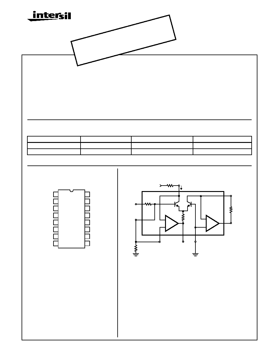
Pinout
ICL8049 (CERDIP)
TOP VIEW
14
15
16
9
13
12
11
10
1
2
3
4
5
7
6
8
A
1
INPUT
GAIN
I
REF
V-
NC
A
1
OUTPUT
V
IN
A
2
INPUT
A
2
OFFSET
V+
V
OUT
NC
GND
NULL
A
2
OFFSET
NULL
A
1
OFFSET
NULL
A
1
OFFSET
NULL
Functional Diagram
ICL8049
V
REF
I
REF
3
1
7
15
10
14
2
16
V
IN
GAIN
A
1
INPUT
A
1
OUTPUT
GND
f
OUT
A
2
INPUT
V
OUT
Q
2
Q
1
A
1
+
-
A
2
+
-
Description
The ICL8049 is a monolithic antilogarithmic amplifier that is
fully temperature compensated and is nominally designed to
provide 1 decade of output voltage for each 1V change of
input voltage. For increased flexibility, the scale factor, refer-
ence current and offset voltage are externally adjustable.
Features
∑ Full Scale Accuracy . . . . . . . . . . . . . . . . . . . . . . . . . 0.5%
∑ Temperature Compensated Operation . . . . 0
o
C to 70
o
C
∑ Scale Factor, Adjustable . . . . . . . . . . . . . . . . 1V/Decade
∑ Dynamic Voltage Range . . . . . . . . . . . . . . . . . . . . .60dB
∑ Dual JFET Input Op Amps
File Number
4768
OBSO
LETE
PRO
DUC
T
NO R
ECO
MME
NDED
REP
LACE
MEN
T
conta
ct ou
r Tec
hnica
l Sup
port
Cent
er at
1-888
-INTE
RSIL
or w
ww.in
tersil
.com
/tsc

2
ICL8049
Absolute Maximum Ratings
Operating Conditions
Supply Voltage
. . . . . . . . . . . . . . . . . . . . . . . . . . . . . . . . . . . . . . . . . ±18V
V
IN
(Input Current)
. . . . . . . . . . . . . . . . . . . . . . . . . . . . . . . . . . . . . . ±15V
I
REF
(Reference Current) . . . . . . . . . . . . . . . . . . . . . . . . . . . . . 2mA
Voltage Between Offset Null and V+ . . . . . . . . . . . . . . . . . . .
±0.5V
Output Short Circuit Duration . . . . . . . . . . . . . . . . . . . . . . . Indefinite
Power Dissipation. . . . . . . . . . . . . . . . . . . . . . . . . . . . . . . . . 750mW
Lead Temperature (Soldering 10 Sec.) . . . . . . . . . . . . . . . . . 300
o
C
Operating Temperature Range . . . . . . . . . . . . . . . . . . . 0
o
C to 70
o
C
Storage Temperature Range . . . . . . . . . . . . . . . . . . -65
o
C to 150
o
C
CAUTION: Stresses above those listed in "Absolute Maximum Ratings" may cause permanent damage to the device. This is a stress only rating and operation
of the device at these or any other conditions above those indicated in the operational sections of this specification is not implied.
Electrical Specifications
V
S
=
±15V, T
A
= 25
o
C, I
REF
= 1mA, Scale Factor Adjusted for 1 Decade (Out) per Volt (In), Unless Oth-
erwise Specified
PARAMETERS
TEST CONDITIONS
ICL4049BC
ICL8049CC
UNITS
MIN
TYP
MAX
MIN
TYP
MAX
Dynamic Range (V
OUT
)
V
OUT
= 10mV to 10V
60
-
-
60
-
-
dB
Error, Absolute Value
0V
V
IN
2V
-
3
15
-
5
25
mV
T
A
= 0
o
C to 70
o
C,
0V
V
IN
3V
-
20
75
-
30
150
mV
Temperature Coefficient, Referred
to V
IN
V
IN
= 3V
-
0.38
-
-
0.55
-
mV/
o
C
Power Supply Rejection Ratio
Referred to Input,
for V
IN
= 0V
-
2.0
-
-
2.0
-
µV/V
Offset Voltage (A
1
and A
2
)
Before Nulling
-
15
25
-
15
50
mV
Wideband Noise
Referred to Input,
for V
IN
= 0V
-
26
-
-
26
-
µV
RMS
Output Voltage Swing
R
L
= 10k
±12
±14
-
±12
±14
-
V
R
L
= 2k
±10
±13
-
±10
±13
-
V
Power Consumption
-
150
200
-
150
200
mW
Supply Current
-
5
6.7
-
5
6.7
mA
3
ICL8049
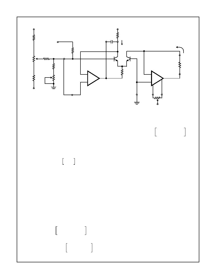
ICL8049 Detailed Description
The ICL8049 relies on the same logarithmic properties of
the transistor as the ICL8048. The input voltage forces a
specific
V
BE
between Q
1
and Q
2
(Figure 1). This V
BE
difference is converted into a difference of collector currents
by the transistor pair. The equation governing the behavior
of the transistor pair is derived from (2) on the previous page
and is as follows:
(1)
When numerical values for q/kT are put into this equation, it
is found that a
V
BE
of 59mV (at +25
o
C) is required to
change the collector current ratio by a factor of ten. But for
ease of application, it is desirable that a 1V change at the
input generate a tenfold change at the output. The required
input attenuation is achieved by the network comprising R
1
and R
2
. In order that scale factors other than one decade
per volt may be selected, R
2
is external to the chip. It should
have a value of 1k
, adjustable ±20%, for one decade per
volt. R
1
is a thin film resistor deposited on the monolithic
chip; its temperature characteristics are chosen to
compensate the temperature dependence of Equation 1, as
explained on the previous page.
The overall transfer function is as follows:
(2)
Substituting V
OUT
= I
OUT
x R
OUT
gives:
(3)
IC1
IC2
--------
exp
q
VBE
kT
------------------
=
I
OUT
I
REF
----------
exp
-R2
R1 R2
+
(
)
---------------------
qVIN
kT
---------
◊
=
VOUT
ROUT IREF exp
R2
≠
R1 R2
+
(
)
-------------------------
qVIN
kT
------------
◊
=
For voltage references Equation 3 becomes
(4)
ICL8049 Offset and Scale Factor
Adjustment
As with the log amplifier, the antilog amplifier requires three
adjustments. The first step is to null out the offset voltage of
A
2
. This is accomplished by reverse biasing the base-emitter
of Q
2
. A
2
then operates as a unity gain buffer with a
grounded input. The second step forces V
IN
= 0; the output is
adjusted for V
OUT
= 10V. This step essentially "anchors" one
point on the transfer function. The third step applies a
specific input and adjusts the output to the correct voltage.
This sets the scale factor. Referring to Figure 1 the exact
procedure for 1 decade/volt is as follows:
1. Connect the input (pin #16) to +15V. This reverse biases
the base-emitter of Q
2
. Adjust R
7
for V
OUT
= 0V. Discon-
nect the input from +15V.
2. Connect the input to Ground. Adjust R
4
for V
OUT
= 10V.
Disconnect the input from Ground.
3. Connect the input to a precise 2V supply and adjust R
2
for
V
OUT
= 100mV.
The procedure outlined above optimizes the performance
over a 3 decade range at the output (i.e., V
OUT
from 10mV)
to 10V). For a more limited range of output voltages, for
example 1V to 10V, it would be better to use a precise 1V
supply and adjust for V
OUT
= 1V. For other scale factors and/
or starting points, different values for R
2
and R
REF
will be
needed, but the same basic procedure applies.
V
OUT
V
REF
R
OUT
R
REF
------------
◊
exp
R
≠
2
R1 R2
+
(
)
---------------------
qVIN
kT
---------
◊
=
FIGURE 1. ICL8049 OFFSET AND SCALE FACTOR ADJUSTMENT
A
1
+
-
A
2
+
-
R
7
2k
V+
1k
200pF
I
REF
13
12
15
3
7
16
1
10
14
Q
1
Q
2
R
5
15k
R
2
R
1
15.9k
2
V
IN
V+
V-
R
REF
15k
C
1
V
REF
(+15V)
I
OUT
V
OUT
R
OUT
10k
R
6
100k
R
3
15k
680
(LOW
T.C.)
R
4
2k