 | –≠–ª–µ–∫—Ç—Ä–æ–Ω–Ω—ã–π –∫–æ–º–ø–æ–Ω–µ–Ω—Ç: ICL8052A | –°–∫–∞—á–∞—Ç—å:  PDF PDF  ZIP ZIP |
1
TM
File Number
3081.2
CAUTION: These devices are sensitive to electrostatic discharge; follow proper IC Handling Procedures.
1-888-INTERSIL or 321-724-7143
|
Intersil and Design is a trademark of Intersil Americas Inc.
|
Copyright © Intersil Americas Inc. 2001
ICL8052A/ICL71C03,
ICL8068A/ICL71C03
Precision 4
1
/
2
Digit, A/D Converter
The ICL8052A or ICL8068A/lCL71C03 chip pairs with their
multiplexed BCD output and digit drivers are ideally suited
for the visual display DVM/DPM market. The outstanding
4
1
/
2
digit accuracy, 200.00mV to 2.0000V full scale
capability, auto-zero and auto-polarity combine with true
ratiometric operation, almost ideal differential linearity and
time-proven dual slope conversion. Use of these chip pairs
eliminates clock feedthrough problems, and avoids the
critical board layout usually required to minimize charge
injection.
When only 2000 counts of resolution are required, the 71C03
can be wired for 3
1
/
2
digits and give up to 30 readings/sec.,
making it ideally suited for a wide variety of applications.
The ICL71C03 is an improved CMOS plug-in replacement for
the lCL7103 and should be used in all new designs.
Features
∑ Typically Less Than 2
µ
V
P-P
Noise (200.00mV Full Scale,
lCL8068A
∑ Accuracy Guaranteed to
±
1 Count Over Entire
±
20,000
Counts (2.0000V Full Scale)
∑ Guaranteed Zero Reading for 0V Input
∑ True Polarity at Zero Count for Precise Null Detection
∑ Single Reference Voltage Required
∑ Over-Range and Under-Range Signals Available for Auto-
Ranging Capability
∑ All Outputs TTL Compatible
∑ Medium Quality Reference, 40ppm (Typ) on Board
∑ Blinking Display Gives Visual Indication of Over Range
∑ Six Auxiliary Inputs/Outputs are Available for Interfacing to
UARTs, Microprocessors or Other Complex Circuitry
∑ 5pA Input Current (Typ) (8052A)
Part Number Information
PART NUMBER
TEMP.
RANGE (
o
C)
PACKAGE
PKG.
NO.
lCL8052ACPD
0 to 70
14 Ld PDIP
E14.3
ICL8068ACDD
0 to 70
14 Ld CERDIP
F14.3
lCL8068ACJD
0 to 70
14 Ld CERDIP
F14.3
lCL71C03ACPl
0 to 70
28 Ld PDIP
E28.6
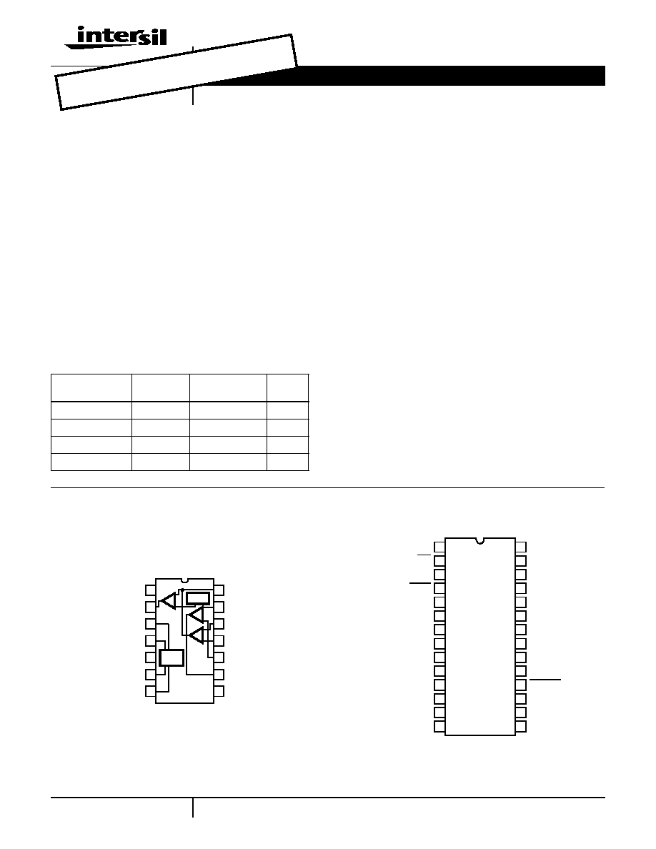
Pinouts
ICL8052A/ICL8068A
(CERDIP, PDIP)
TOP VIEW
ICL71C03 (PDIP)
TOP VIEW
V-
COMP OUT
REF CAP
REF BYPASS
GND
REF OUT
REF SUPPLY
INT OUT
+BUFF IN
+INT IN
-INT IN
-BUFF IN
BUFF OUT
V+
1
2
3
4
5
6
7
14
13
12
11
10
9
8
-1.2V
V
REF
ICL8052A/
ICL8068A
V+
4
1
/
2
/ 3
1
/
2
POL
RUN/HOLD
COMP IN
V-
REFERENCE
REF. CAP. 1
REF. CAP. 2
ANALOG IN
ANALOG GND
CLOCK IN
UNDER-RANGE
OVER-RANGE
BUSY
D
2
D
3
D
4
B
8
(MSB)
B
2
D
5
(MSD)
STROBE
A-Z IN
A-Z OUT
DIGITAL GND
D
1
(LSD)
B
4
B
1
(LSB)
28
27
26
25
24
23
22
21
20
19
18
17
16
15
1
2
3
4
5
6
7
8
9
10
11
12
13
14
Data Sheet
May 2001
itle
L80
AA/
L71
3,
L80
A/IC
1C0
bjec
ecis
/2
git,
D
nver
)
utho
)
eyw
s
tersi
rpor
on,
alog
gital
nver
,
D,
crop
esso
erfa
ta
quis
OBSO
LETE
PROD
UCT
NO RE
COMM
ENDE
D REP
LACE
MENT
2
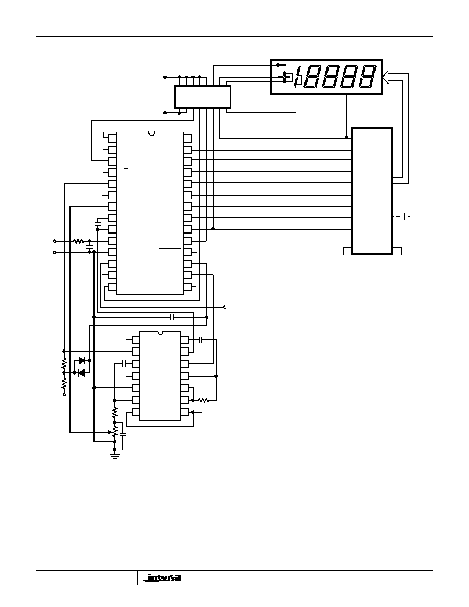
Functional Block Diagram
FIGURE 1.
A2
+
-
A3
+
-
INTEG.
COMP.
A1
+
-
BUFFER
14
11
9
INT OUT
-INT IN
BUF OUT
10
-BUF IN
-1.2V
2
1
-15V
7
8
+15V
12
+INT IN
13
ICL8052A/8068A
INT.
REF.
6
3
+BUF IN
5
REF
OUT
10k
1k
300pF
10
µ
F
COMP
OUT
COMP IN
5
16
9
MULTIPLEXER
COUNTERS
20
CONTROL LOGIC
ZERO
CROSSING
DETECTOR
21
22
23
ICL71C03
REF
AZ OUT
SW3
1
+5V
ANALOG
GND
ANALOG
INPUT
28
BUSY
18
STROBE
13
UNDER
14
12
CLOCK
2
4 1/2 DIGIT/
2
6
5
1
4
10
µ
F (TYP)
CAP 2
REF
CAP 1
8
7
10
11
10k
0.1
µ
F
REF
1
µ
F (TYP)
17
AZ IN
6
-15V
15
0.22
µ
F
10k
90k
100k
4
IN
RUN/
HOLD
RANGE
OVER
RANGE
3 1/2 DIGIT
B
1
B
2
B
3
B
4
LATCH
LATCH
LATCH
LATCH
LATCH
LSD
MSD
SEVEN-
SEGMENT
DECODER
3
P
O
L
ARIT
Y
19
24
25
26
27
D
5
D
4
D
3
D
2
D
1
ICL8052A/ICL71C03, ICL8068A/ICL71C03
3
Absolute Maximum Ratings
Thermal Information
ICL8052A, ICL8068A
Supply Voltage . . . . . . . . . . . . . . . . . . . . . . . . . . . . . . . . . . . . .
±
18V
Differential Input Voltage
(8068A). . . . . . . . . . . . . . . . . . . . . . . . . . . . . . . . . . . . . . . . .
±
30V
(8052A). . . . . . . . . . . . . . . . . . . . . . . . . . . . . . . . . . . . . . . . . .
±
6V
Input Voltage (Note 1) . . . . . . . . . . . . . . . . . . . . . . . . . . . . . . .
±
15V
Output Short Circuit Duration All Outputs (Note 2) . . . . . . Indefinite
ICL71C03
Power Supply Voltage (GND to V+). . . . . . . . . . . . . . . . . . . . . . 6.5V
Negative Supply Voltage (GND to V-) . . . . . . . . . . . . . . . . . . . . -17V
Analog Input Voltage (Note 3) . . . . . . . . . . . . . . . . . . . . . . . V+ to V-
Digital Input Voltage (Note 4) . . . . . . . . .(GND - 0.3V) to (V+ + 0.3V)
Operating Conditions
Temperature Range . . . . . . . . . . . . . . . . . . . . . . . . . . . . 0
o
C to 70
o
C
Thermal Resistance (Typical, Note 5)
JA
(
o
C/W)
JC
(
o
C/W)
CERDIP Package. . . . . . . . . . . . . . . . .
75
20
14 Ld PDIP Package . . . . . . . . . . . . . .
100
N/A
28 Ld PDIP Package . . . . . . . . . . . . . .
65
N/A
Maximum Storage Temperature. . . . . . . . . . . . . . . . -65
o
C to 150
o
C
Maximum Lead Temperature (Soldering, 10s). . . . . . . . . . . . . 300
o
C
CAUTION: Stresses above those listed in "Absolute Maximum Ratings" may cause permanent damage to the device. This is a stress only rating and operation of the
device at these or any other conditions above those indicated in the operational sections of this specification is not implied.
NOTES:
1.
JA
is measured with the component mounted on a low effective thermal conductivity test board in free air. See Tech Brief TB379 for details.
2. For supply voltages less than
±
15V, the absolute maximum input voltage is equal to the supply voltage.
3. Short circuit may be to ground or either supply. Rating applies to 70
o
C ambient temperature.
4. Input voltages may exceed the supply voltages provided the input current is limited to
±
100
µ
A.
5. Connecting any digital inputs or outputs to voltages greater then V+ or less than GND may cause destructive device latchup. For this reason it
is recommended that the power supply to the ICL71C03 be established before any inputs from sources not on that supply are applied.
6.
JA
is measured with the component mounted on an evaluation PC board in free air.
Electrical Specifications
PARAMETER
SYMBOL
TEST
CONDITIONS
MIN
TYP
MAX
UNITS
Clock In, Run/Hold, 4 1/2 / 3 1/2
I
INL
V
IN
= 0
-
0.2
0.6
mA
I
INH
V
IN
= +5V
-
0.1
10
µ
A
Comp. In Current
I
INL
V
IN
= 0
-
0.1
10
µ
A
I
INH
V
IN
= +5V
-
0.1
10
µ
A
Threshold Voltage
V
INTH
-
2.5
-
V
All Outputs
V
OL
I
OL
= 1.6mA
-
0.25
0.40
V
B
1
, B
2
, B
4
, B
8
, D
1
, D
2
, D
3
, D
4
, D
5
V
OH
I
OH
= -1mA
2.4
4.2
-
V
Busy, Strobe, Over-Range, Under-Range Polarity
V
OH
I
OH
= -10
µ
A
4.9
4.99
-
V
Switches 1, 3, 4, 5, 6
r
DS(ON)
-
400
-
Switch 2
r
DS(ON)
-
1200
-
Switch Leakage (All)
I
D(OFF)
-
2
-
pA
+5V Supply Range
V+
4
5
6
V
-15V Supply Range
V-
-5
-15
-18
V
+5V Supply Current
I+
f
CLK
= 0
-
1.1
3
mA
-15V Supply Current
I-
f
CLK
= 0
-
0.8
3
mA
Power Dissipation Capacitance
C
PD
vs Clock Frequency
-
40
-
pF
Clock Frequency (Note 6)
DC
2000
1200
kHz
NOTE:
7. This specification relates to the clock frequency range over which the ICL71C03A will correctly perform its various functions. See the "Max Clock
Frequency" section under Component Value Selection for limitations on the clock frequency range in a system.
ICL8052A/ICL71C03, ICL8068A/ICL71C03
4
ICL8068A Electrical Specifications
V
SUPPLY
=
±
15V, T
A
= 25
o
C, Unless Otherwise Specified
PARAMETER
SYMBOL
TEST
CONDITIONS
MIN
TYP
MAX
UNITS
EACH OPERATIONAL AMPLIFIER
Input Offset Voltage
V
OS
V
CM
= 0V
-
20
65
mV
Input Current (Either Input) (Note 7)
I
IN
V
CM
= 0V
-
80
150
pA
Common-Mode Rejection Ratio
CMRR
V
CM
=
±
10V
70
90
-
dB
Non-Linear Component of Common-Mode Rejection
Ratio (Note 8)
V
CM
=
±
2V
-
110
-
dB
Large Signal Voltage Gain
A
V
R
L
= 50k
20,000
-
-
V/V
Slew Rate
SR
-
6
-
V/
µ
s
Unity Gain Bandwidth
GBW
-
2
-
MHz
Output Short-Circuit Current
I
SC
-
5
-
mA
COMPARATOR AMPLIFIER
Small-Signal Voltage Gain
A
VOL
R
L
= 30k
-
-
-
V/V
Positive Output Voltage Swing
+V
O
12
13
-
V
Negative Output Voltage Swing
-V
O
-2.0
-2.6
-
V
VOLTAGE REFERENCE
Output Voltage
V
O
1.60
1.75
1.90
V
Output Resistance
R
O
-
5
-
Temperature Coefficient
TC
-
40
-
ppm/
o
C
Supply Voltage (V++ -V-)
V
SUPPLY
±
10
-
±
16
V
Supply Current Total
I
SUPPLY
-
8
14
mA
ICL8052A Electrical Specifications
V
SUPPLY
=
±
15V, T
A
= 25
o
C, Unless Otherwise Specified
PARAMETER
SYMBOL
TEST
CONDITIONS
MIN
TYP
MAX
UNITS
EACH OPERATIONAL AMPLIFIER
Input Offset Voltage
V
OS
V
CM
= 0V
-
20
75
mV
Input Current (Either Input) (Note 7)
I
IN
V
CM
= 0V
-
2
10
pA
Common-Mode Rejection Ratio
CMRR
V
CM
=
±
10V
70
90
-
dB
Non-Linear Component of Common-Mode Rejection
Ratio (Note 8)
V
CM
=
±
2V
-
110
-
dB
Large Signal Voltage Gain
A
V
R
L
= 50k
20,000
-
-
V/V
Slew Rate
SR
-
6
-
V/
µ
s
Unity Gain Bandwidth
GBW
-
1
-
MHz
Output Short-Circuit Current
I
SC
-
20
-
mA
COMPARATOR AMPLIFIER
Small-Signal Voltage Gain
A
VOL
R
L
= 30k
-
-
-
V/V
Positive Output Voltage Swing
+V
O
12
13
-
V
Negative Output Voltage Swing
-V
O
-2.0
-2.6
-
V
VOLTAGE REFERENCE
Output Voltage
V
O
1.60
1.75
1.90
V
Output Resistance
R
O
-
5
-
ICL8052A/ICL71C03, ICL8068A/ICL71C03
5
Temperature Coefficient
TC
-
40
-
ppm/
o
C
Supply Voltage (V++ -V-)
V
SUPPLY
±
10
-
±
16
V
Supply Current Total
I
SUPPLY
-
6
14
mA
NOTES:
8. The input bias currents are junction leakage currents which approximately double for every 10
o
C increase in the junction temperature, T
J
. Due
to limited production test time, the input bias currents are measured with junctions at ambient temperature. In normal operation the junction
temperature rises above the ambient temperature as a result of internal power dissipation, P
D
. T
J
= T
A
+ R
JA
P
D
, where R
JA
is the thermal
resistance from junction to ambient. A heat sink can be used to reduce temperature rise.
9. This is the only component that causes error in dual-slope converter.
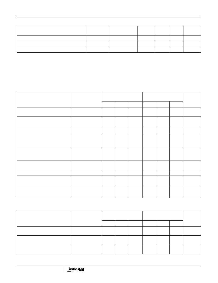
System Electrical Specifications: ICL8068A/ICL71C03
V++ = +15V, V+ = +5V, V- = -15V, T
A
= 25
o
C, f
CLK
Set for 3 Readings/Sec.
PARAMETER
TEST
CONDITIONS
ICL8068A/ICL71C03
(NOTE 9)
ICL8068A/ICL71C03
(NOTE 10)
UNITS
MIN
TYP
MAX
MIN
TYP
MAX
Zero Input Reading
V
IN
= 0V,
Full Scale = 200mV
-000.0
±
000.0
+000.0
-000.0
±
000.0
000.0
Digital
Reading
Ratiometric Error (Note 11)
V
IN
= V
REF
Full Scale = 2V
0.999
1.000
1.001
0.9999
1.0000
1.0001
Digital
Reading
Linearity Over
±
Full Scale (Error of
Reading from Best Straight Line)
-2V
V
IN
+2V
-
0.2
1
-
0.5
1
Counts
Differential Linearity (Difference between
Worst Case Step of Adjacent Counts and
Ideal Step)
-2V
V
IN
+2V
-
0.01
-
-
0.01
-
Counts
Rollover Error (Difference in Reading for
Equal Positive & Negative Voltage Near
Full Scale)
-V
IN
+V
IN
2V
-
0.2
1
-
0.5
1
Counts
Noise (P-P Value Not Exceeded 95% of
Time)
V
IN
= 0V,
Full Scale = 200mV
-
3
-
-
2
-
µ
V
Leakage Current at Input
V
IN
= 0V
-
200
300
-
100
200
pA
Zero Reading Drift (Note 12)
V
IN
= 0V,
0
o
C
T
A
50
o
C
-
1
5
-
0.5
2
µ
V/
o
C
Scale Factor Temperature Coefficient
(Note 12)
V
IN
= 2V,
0
o
C
T
A
50
o
C
Ext. Ref. 0ppm/
o
C
-
3
15
-
2
5
ppm/
o
C
System Electrical Specifications: ICL8052A/ICL71C03
V++ = +15V, V+ = +5V, V- = -15V, T
A
= 25
o
C, f
CLK
Set for 3 Reading/Sec.
PARAMETER
TEST
CONDITIONS
ICL8052A/ICL71C03
(NOTE 9)
ICL8052A/A/ICL71C03
(NOTE 10)
UNITS
MIN
TYP
MAX
MIN
TYP
MAX
Zero Input Reading
V
IN
= 0V,
Full Scale = 2V
-0.000
±
0.000
+0.000
-0.000
±
0.000
0.000
Digital
Reading
Ratiometric Error (Note 11)
V
IN
= V
REF
Full Scale = 2V
0.999
1.000
1.001
0.9999
1.0000
1.0001
Digital
Reading
Linearity Over
±
Full Scale (Error of
Reading from Best Straight Line)
-2V
V
IN
+2V
-
0.2
1
-
0.5
1
Counts
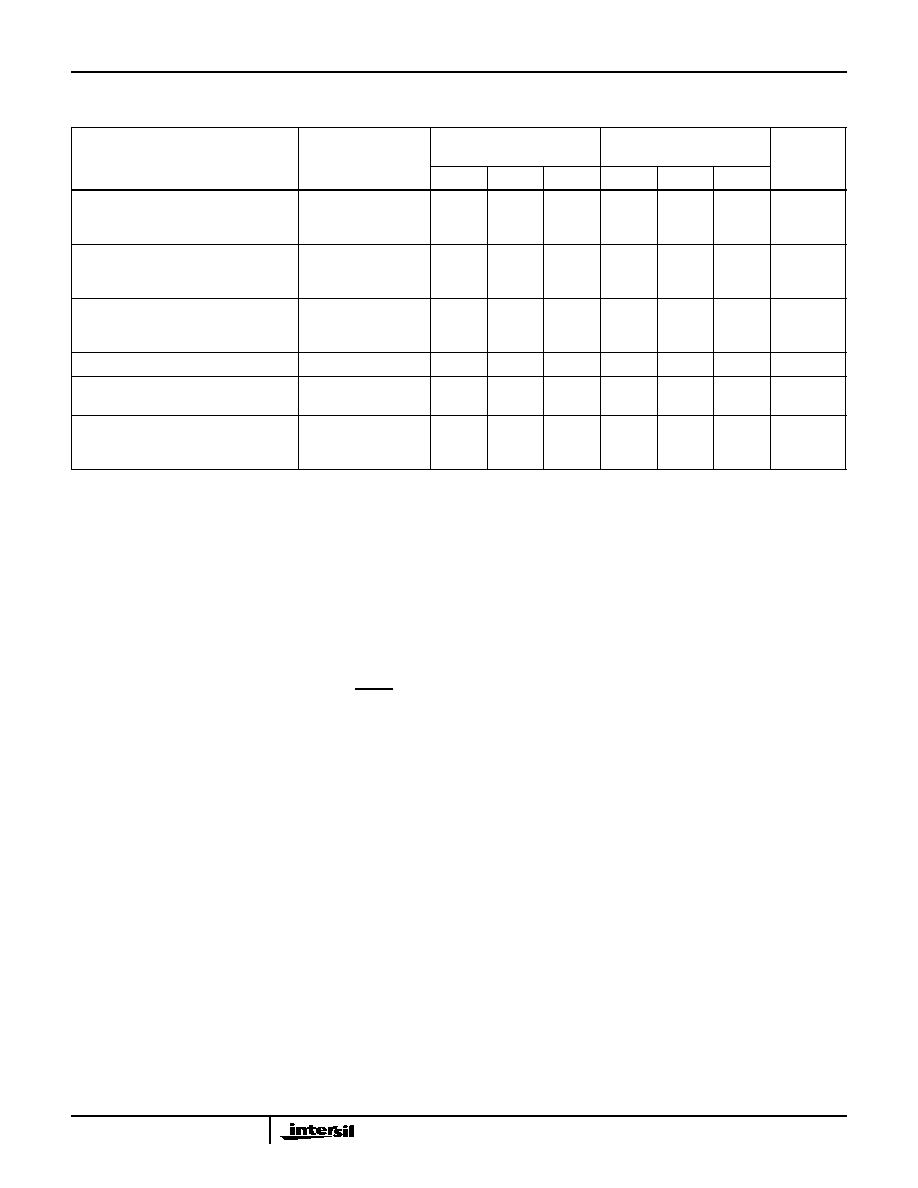
ICL8052A Electrical Specifications
V
SUPPLY
=
±
15V, T
A
= 25
o
C, Unless Otherwise Specified (Continued)
PARAMETER
SYMBOL
TEST
CONDITIONS
MIN
TYP
MAX
UNITS
ICL8052A/ICL71C03, ICL8068A/ICL71C03
6
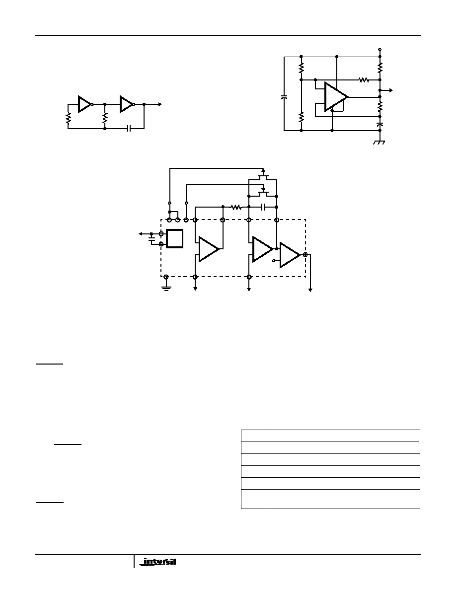
Detailed Description
Analog Section
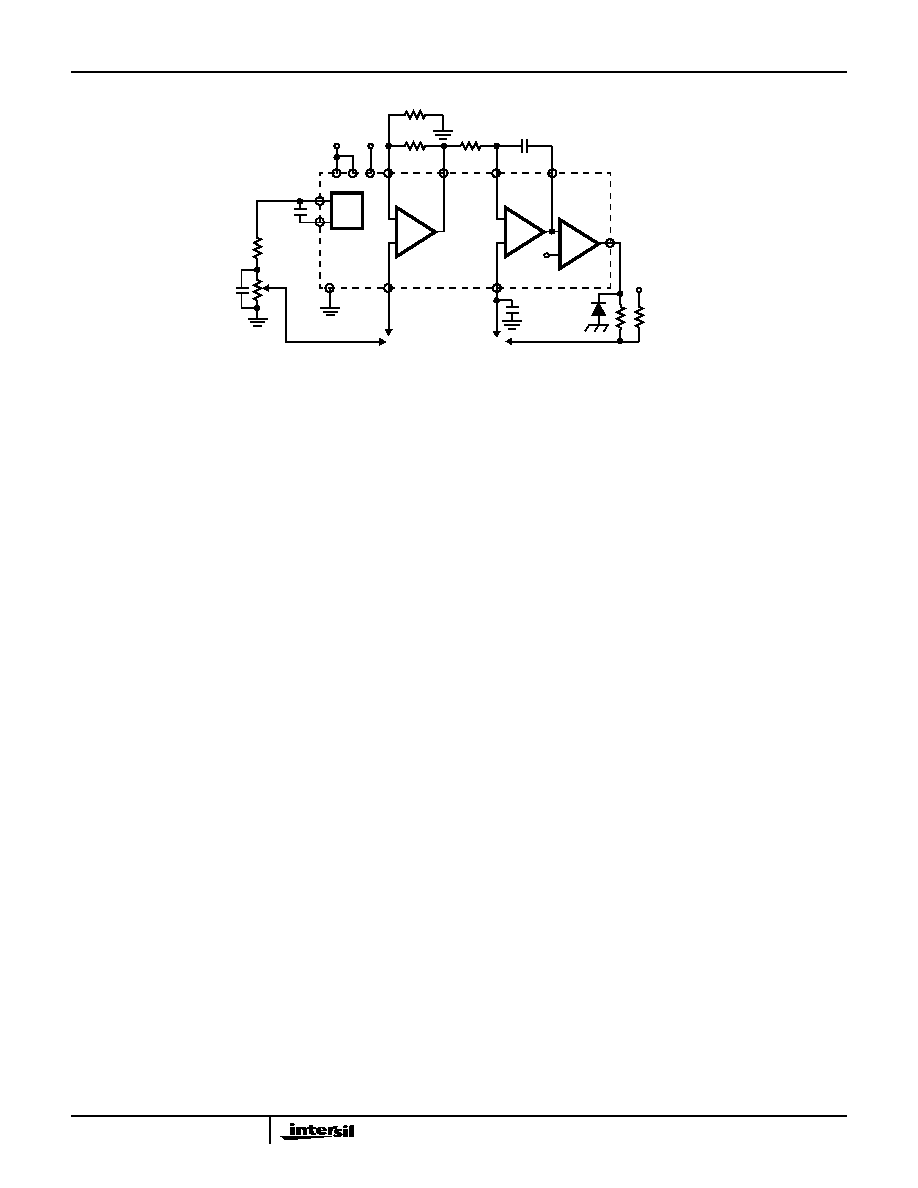
Figure 2 shows the equivalent Circuit of the Analog Section
of both the ICL71C03/8052A and the ICL71C03/8068A in
the 3 different phases of operation. IF the RUN/HOLD pin is
left open or tied to V+, the system will perform conversions
at a rate determined by the clock frequency: 40,0002 at 4
1
/
2
digit and 4002 at 3
1
/
2
digit clock periods per cycle (see
Figure 3 for details of conversion timing).
Auto-Zero Phase I
(Figure 2A)
During the Auto-Zero, the input of the buffer is connected to
V
REF
through switch 2, and switch 3 closes a loop around
the integrator and comparator, the purpose of which is to
charge the auto-zero capacitor until the integrator output
does not change with time. Also, switches 1 and 2 recharge
the reference capacitor to V
REF
.
Input Integrate Phase II
(Figure 2B)
During Input Integrate the auto-zero loop is opened and the
ANALOG INPUT is connected to the BUFFER INPUT
through switch 4 and C
REF
. If the input signal is zero, the
buffer, integrator and comparator will see the same voltage
that existed in the previous state (Auto-Zero). Thus, the
integrator output will not change but will remain stationary
during the entire Input Integrate cycle. If V
IN
is not equal to
zero, and unbalanced condition exists compared to the Auto
Zero phase, and the integrator will generate a ramp whose
slope is proportional to V
IN
. At the end of this phase, the
sign of the ramp is latched into the polarity F/F.
Deintegrate Phase II
(Figures 2C and 2D)
During the Deintegrate phase, the switch drive logic uses the
output of the polarity F/F in determining whether to close
switch 6 or 5. If the input signal is positive, switch 6 is closed
and a voltage which is V
REF
more negative than during
Auto-Zero is impressed on the BUFFER INPUT. Negative
Inputs will cause +2(V
REF
) to be applied to the BUFFER
INPUT via switch 5. Thus, the reference capacitor generates
the equivalent of a (+) or (-) reference from the single
reference voltage with negligible error. The reference voltage
returns the output of the integrator to the zero-crossing point
established in Phase I. The time, or number of counts,
required to do this is proportional to the input voltage. Since
the Deintegrate phase can be twice as long as the Input
Integrate Phase, the input voltage required to give a full
scale reading is 2V
REF
.
Differential Linearity (Difference between
Worst Case Step of Adjacent Counts and
Ideal Step)
-2V
V
IN
+2V
-
0.01
-
-
0.01
-
Counts
Rollover Error (Difference in Reading for
Equal Positive & Negative Voltage Near
Full Scale)
-V
IN
+V
IN
2V
-
0.2
1
-
0.5
1
Counts
Noise (Peak-To-Peak Value Not
Exceeded 95% of Time)
V
IN
= 0V,
Full Scale = 200mV,
Full Scale = 2V
-
20
50
-
-
-
-
30
-
-
µ
V
Leakage Current at Input
V
IN
= 0V
-
5
30
-
3
10
pA
Zero Reading Drift
V
IN
= 0V,
0
o
C To 70
o
C
-
1
5
-
0.5
2
µ
V/
o
C
Scale Factor Temperature Coefficient
V
IN
= 2V,
0
o
C To 70
o
C,
Ext. Ref. 0ppm/
o
C
-
3
15
-
2
5
ppm/
o
C
NOTES:
10. Tested in 3
1
/
2
digit (2,000 count) circuit shown in Figure 5, clock frequency 12kHz. Pin 2 71C03 connected to GND.
11. Tested in 4
1
/
2
digit (20,000 count) circuit shown in Figure 5, clock frequency 120kHz. Pin 2 71C03A open.
12. Tested with a low dielectric absorption integrating capacitor. See Component Selection Section.
13. The temperature range can be extended to 70
o
C and beyond if the Auto-Zero and Reference capacitors are increased to absorb the high
temperature leakage of the 8068A.
System Electrical Specifications: ICL8052A/ICL71C03
V++ = +15V, V+ = +5V, V- = -15V, T
A
= 25
o
C, f
CLK
Set for 3 Reading/Sec. (Continued)
PARAMETER
TEST
CONDITIONS
ICL8052A/ICL71C03
(NOTE 9)
ICL8052A/A/ICL71C03
(NOTE 10)
UNITS
MIN
TYP
MAX
MIN
TYP
MAX
ICL8052A/ICL71C03, ICL8068A/ICL71C03
7
FIGURE 2A. PHASE I AUTO-ZERO
FIGURE 2B. PHASE II INTEGRATE INPUT
FIGURE 2C. PHASE III + DEINTEGRATE
FIGURE 2D. PHASE III - DEINTEGRATE
FIGURE 2. ANALOG SECTION OF EITHER ICL8052A OR ICL8068A WITH ICL71C03
A2
+
-
A3
+
-
INTEGRATOR
COMPARATOR
A1
+
-
BUFFER
C
INT
3
R
INT
C
AZ
ZERO
CROSSING
DETECTOR
2
6
5
1
V
REF
(+1.000V)
C
REF
4
C
STRAY
V
IN
1
µ
F
A2
+
-
A3
+
-
INTEGRATOR
COMPARATOR
A1
+
-
BUFFER
C
INT
3
R
INT
C
AZ
ZERO
CROSSING
DETECTOR
2
6
5
1
V
REF
(+1.000V)
C
REF
4
C
STRAY
V
IN
1
µ
F
POLARITY
FF
A2
+
-
A3
+
-
INTEGRATOR
COMPARATOR
A1
+
-
BUFFER
C
INT
3
R
INT
C
AZ
ZERO
CROSSING
DETECTOR
2
6
5
1
V
REF
(+1.000V)
C
REF
4
C
STRAY
V
IN
1
µ
F
POLARITY
FF
A2
+
-
A3
+
-
INTEGRATOR
COMPARATOR
A1
+
-
BUFFER
C
INT
3
R
INT
C
AZ
ZERO
CROSSING
DETECTOR
2
6
5
1
V
REF
(+1.000V)
C
REF
4
C
STRAY
V
IN
1
µ
F
POLARITY
FF
ICL8052A/ICL71C03, ICL8068A/ICL71C03

8
Zero-Crossing Flip-Flop
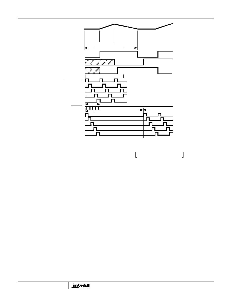
Figure 4 shows the problem that the zero-crossing F/F is
designated to solve.
The integrator output is approaching the zero-crossing point
where the count will be latched and the reading displayed.
For a 20,000 count instrument, the ramp is changing
approximately 0.50mV per clock pulse (10V Max integrator
output divided by 20,000 counts). The clock pulse
feedthrough superimposed upon this ramp would have to be
less than 100mV peak to avoid causing significant errors.
The flip-flop interrogates the data once every clock pulse
after the transients of the previous clock pulse and half-clock
pulse have died down. False zero-crossings caused by clock
pulses are not recognized. Of course, the flip-flop delays the
true zero-crossing by one count in every instance, and if a
correction were not made, the display would always be one
count too high. Therefore, the counter is disabled for one
clock pulse at the beginning of phase 3. This one count
delay compensates for the delay of the zero crossing flip-
flop, and allows the correct number to be latched into the
display. Similarly, a one count delay at the beginning of
phase 1 gives an overload display of 0000 instead of 0001.
No delay occurs during phase 2, so that true ratiometric
readings result.
Detailed Description
Digital Section
The 71C03 includes several pins which allow it to operate
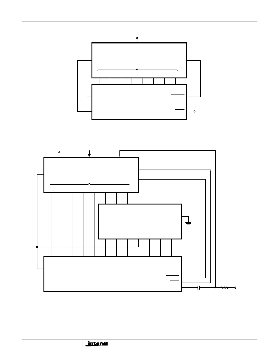
conveniently in more sophisticated systems. These include:
4-1/2 / 3-1/2 (PIN 2)
When high (or open) the internal counter operates as a full
4
1
/
2
decade counter, with a complete measurement cycle
requiring 40,002 counts. When held low, the least significant
decade is cleared and the clock is fed directly into the next
decade. A measurement cycle now requires only 4,0002
clock pulses. All 5 digit drivers are active in either case, with
each digit lasting 200 counts with Pin 2 high (4
1
/
2
digit) and
20 counts for Pin 2 low (3
1
/
2
digit).
FIGURE 3. CONVERSION TIMING
POLARITY
DETECTED
ZERO CROSSING
OCCURS
ZERO CROSSING
DETECTED
DEINT PHASE III
INT PHASE II
AZ PHASE I
AZ
INTEGRATOR
OUTPUT
CLOCK
INTERNAL LATCH
BUSY OUTPUT
NUMBER OF COUNTS TO ZERO CROSSING
PROPORTIONAL TO V
IN
AFTER ZERO CROSSING,
ANALOG SECTION WILL
BE IN AUTOZERO
CONFIGURATION
COUNTS
PHASE I
PHASE II
PHASE III
4
1
/
2
DIGIT
10,001
10,000
20,001
3
1
/
2
DIGIT
1,001
1,000
2,001
FIGURE 4. INTEGRATOR OUTPUT NEAR ZERO-CROSSING
TRUE ZERO
CROSSING
CLOCK
PULSE
FEEDTHROUGH
FALSE ZERO
CROSSING
ICL8052A/ICL71C03, ICL8068A/ICL71C03
9
RUN/HOLD (PIN 4)
When high (or open) the A/D will free-run with equally
spaced measurement cycles every 40,0002 /4,002 clock
pulses. If taken low, the converter will continue the full
measurement cycle that it is doing and then hold this reading
as long as Pin 4 is held low. A short positive pulse (greater
then 300ns) will now initiate a new measurement cycle
beginning with up to 10,001 /1,001 counts of auto zero. Of
course if the pulse occurs before the full measurement cycle
(40,002 /4,002 counts) is completed, it will not be recognized
and the converter will simply complete the measurement it is
doing. An external indication that full measurement cycle
has been completed is that the first STROBE pulse (see
below) will occur 101 / 11 counts after the end of this cycle.
Thus, if RUN/HOLD is low and has been low for at least
101 / 11 counts, converter is holding and ready to start a new
measurement when pulsed high.
STROBE (PIN 18)
This is a negative-going output pulse that aids in transferring
the BCD data to external latches, UARTs or
microprocessors. There are 5 negative-going STROBE
pulses that occur once and only once for each measurement
cycle starting 101 /11 pulses after the end of the full
measurement cycle. Digit 5 (MSD) goes high at the end of
the measurement cycle and stays on for 201 / 21 counts. In
the center of this digit pulse (to avoid race conditions
between changing BCD and digit drives) the first STROBE
pulse goes negative for
1
/
2
clock pulse width. Similarly, after
Digit 5, Digit 4 goes high (for 200 / 20 clock pulses) and
100 / 10 pulses later the STROBE goes negative for the
second time. This continues through Digit 1 (LSD) when the
fifth and last STROBE pulse is sent. The digit drive will
continue to scan (unless the previous signal was over-range)
but no additional STROBE pulses will be sent until a new
measurement is available.
BUSY (PIN 28)
BUSY goes high at the beginning of signal integrate and
stays high until the first clock pulse after zero-crossing (or
after end of measurement in the case of an OVER-RANGE).
The internal latches are enabled (i.e., loaded) during the first
clock pulse after BUSY and are latched at the end of this
clock pulse. The circuit automatically reverts to auto-zero
when not BUSY so it may also be considered an A-Z signal.
A very simple means for transmitting the data down a single
wire pair from a remote location would be to AND BUSY with
clock and subtract 10,001 /1,001 counts from the number of
pulses received - as mentioned previously there is one "NO-
count" pulse in each Reference Integrate cycle.
OVER-RANGE (PIN 4)
This pin goes positive when the input signal exceeds the
range (20,000 /2,000) of the converter. The output F-F is set
at the end of BUSY and is reset to zero at the beginning of
Reference Integrate in the next measurement cycle.
UNDER-RANGE (PIN 13)
This pin goes positive when the reading is 9% of range or
less. The output F-F is set at the end of BUSY (if the new
reading is 1800 /180 or less) and is reset a the beginning of
Signal Integrate of the next reading.
POLARITY (PIN 3)
This pin is positive for a positive input signal. It is valid even for a
zero reading. In other words, +0000 means the signal is
positive but less than the least significant bit. The converter can
be used as null detector by forcing equal (+) and (-) readings.
The null at this point should be less than 0.1 LSB. This output
becomes valid at the beginning of Reference Integrate and
remains correct until it is revalidated for the next measurement.
DIGIT DRIVES (PINS 19, 24, 25, 26, AND 27)
Each digit drive is a positive-going signal which lasts for
200 / 20 clock pulses. The scan sequence is D
5
(MSD), D
4
,
D
3
, D
2
, and D
1
(LSD). All five digits are scanned even when
operating in the 3
1
/
2
digit mode, and this scan is continuous
unless and OVER-RANGE occurs. Then all Digit drives are
blanked from the end of the STROBE sequence until the
beginning of Reference Integrate, at which time D
5
will start
the scan again. This gives a blinking display as a visual
indication of OVER-RANGE.
BCD (PINS 20, 21, 22 AND 23)
The Binary coded decimal bit B
8
, B
4
, B
2
, and B
1
are positive
logic signals that go on simultaneously with the Digit driver.
ICL8052A/ICL71C03, ICL8068A/ICL71C03
10
Component Value Selection
For optimum performance of the analog section, care must
be taken in the selection of values for the integrator capacitor
and resistor, auto-zero capacitor, reference voltage, and
conversion rate. These values must be chosen to suit the
particular application.
Integrating Resistor
The integrating resistor is determined by the full scale input
voltage and the output current of the buffer used to charge
the integrator capacitor. This current should be small
compared to the output short circuit current such that
thermal effects are kept to a minimum and linearity is not
affected. Values of 5
µ
A to 40
µ
A give good results with a
nominal of 20
µ
A. The exact value may be chosen by:
NOTE: If gain is used in the buffer amplifier, then:
Integrating Capacitor
The product of integrating resistor and capacitor is selected
to give 9V swing for full scale inputs. This is a compromise
between possibly saturating the integrator (at +14V) due to
tolerance buildup between the resistor, capacitor and clock
and the errors a lower voltage swing could induce due to
offsets referred to the output of the comparator. In general,
the value of C
INT
is given by:
A very important characteristic of the integrating capacitor is
that it has low dielectric absorption to prevent roll-over or
ratiometric errors. A good test for dielectric absorption is to
use the capacitor with the input tied to the reference.
This ratiometric condition should be read half scale 1.0000,
and any deviation is probably due to dielectric absorption.
Polypropylene capacitors give undetectable errors at
reasonable cost. Polystyrene and polycarbonate capacitors
may be used in less critical applications.
Auto-Zero and Reference Capacitor
The size of the auto-zero capacitor has some influence on
the noise of the system, with a larger value capacitor giving
less noise. The reference capacitor should be large enough
such that stray capacitance to ground from its nodes is
negligible.
When gain is used in the buffer amplifier the reference
capacitor should be substantially larger than the auto-zero
capacitor. As a rule of thumb, the reference capacitor should
be approximately the gain times the value of the auto-zero
capacitor. The dielectric absorption of the reference cap and
auto-zero cap are only important at power-on or when the
circuit is recovering from an overload. Thus, smaller or
cheaper caps can be used here if accurate readings are not
required for the first few seconds of recovery.
FIGURE 5. TIMING DIAGRAM FOR OUTPUTS
AUTO
COUNTS
10,001
INTEGRATOR
BUSY
SIGNAL
COUNTS
10,000
INTEG.
REFERENCE
COUNTS MAX
20,001 / 2,001
INTEGRATE
D
5
D
4
D
3
D
2
D
1
AUTO ZERO
DIGIT SCAN
FOR OVER-RANGE
SIGNAL
INTEGRATE
REFERENCE
INTEGRATE
D
1
D
2
D
3
D
4
D
5
FIRST D
5
OF AZ AND REF INT
ONE COUNT LONGER
STROBE
1000
/100 COUNTS
DIGIT SCAN
FOR OVER-RANGE
EXPANDED SCALE BELOW
/ 1,000
OVER-RANGE
WHEN APPLICABLE
UNDER-RANGE
WHEN APPLICABLE
OUTPUT
/ 1,001
ZERO
FULL MEASUREMENT CYCLE
40,002/4,002 COUNTS
R
I NT
Full Scale Voltage (See Note)
20
µ
A
-------------------------------------------------------------------------------
=
R
IN T
Bu fferGa in
(
)
(Full Scale Voltage)
20
µ
A
--------------------------------------------------------------------------------------------
=
C
I NT
10,000(4-1/2 Digit)
1000(3-1/2 Digit)
Clock Period
◊
20
µ
A
(
)
◊
Integrator Output Voltage Swing
-------------------------------------------------------------------------------------------------------------------------
=
ICL8052A/ICL71C03, ICL8068A/ICL71C03
11
Reference Voltage
The analog input required to generate a full scale output is:
V
IN
= 2V
REF
.
The stability of the reference voltage is a major factor in the
overall absolute accuracy of the converter. For this reason, it
is recommended that an external high quality reference be
used where ambient temperature is not controlled or where
high-accuracy absolute measurements are being made.
Buffer Gain
At the end of the auto-zero interval, the instantaneous noise
voltage on the auto-zero capacitor is stored and subtracted
from the input voltage while adding to the reference voltage
during the next cycle. The result of this is that the noise
voltage is effectively somewhat greater than the input noise
voltage of the buffer itself during integration. By introducing
some voltage gain into the buffer, the effect of the auto-zero
noise (referred to the input) can be reduced to the level of
the inherent buffer noise. This generally occurs with a buffer
gain of between 3 and 10. Further increase in buffer gain
merely increases the total offset to be handled by the auto-
zero loop, and reduces the available buffer and integrator
swings, without improving the noise performance of the
system. The circuit recommended for doing this with the
ICL8068A/ICL71C03 is shown in Figure 6.
ICL8052A vs ICL8068A
The ICL8052A offers significantly lower input leakage
currents than the ICL8068A, and may be found preferable in
systems with high input impedances. However, the
ICL8068A has substantially lower noise voltage, and is the
device of choice for systems where noise is a limiting factor,
particularly in low signal level conditions.
Max Clock Frequency
The maximum conversion rate of most dual-slope A/D
converters is limited by frequency response of the
comparator. The comparator in this circuit is no exception,
even though it is entirely NPN with an open-loop, gain-
bandwidth product of 300MHz. The comparator output
follows the integrator ramp with a 3
µ
s delay, and at a clock
frequency of 160kHz (6
µ
s period) half of the first reference
integrate clock period is lost in delay. This means that the
meter reading will change from 0 to 1 with 50
µ
V input, 1 to 2
with 150
µ
V, 2 to 3 at 250
µ
V, etc. This transition at midpoint is
considered desirable by most users. However, if the clock
frequency is increased appreciably above 160kHz, the
instrument will flash "1" on noise peaks even when the input
is shorted.
For many dedicated applications where the input signal is
always on one polarity, the dealy of the comparator need not
be limitation. Since the non-linearity and noise do not
increase substantially with frequency, clock rates of up to
approximately 1MHz may be used. For a fixed clock
frequency, the extra count or counts caused by comparator
delay will be a constant and can be subtracted out digitally.
The minimum clock frequency is established by leakage on
the auto-zero and reference caps. With most devices,
measurement cycles as long as 10 seconds give no
measurable leakage error.
To achieve maximum rejection of 60Hz pickup, the signal
integrate cycle should be a multiple of 60Hz. Oscillator
frequencies of 300kHz, 200kHz, 150kHz, 120kHz, 100kHz,
40kHz, 33
1
/
3
kHz, etc, should be selected. For 50Hz
rejection, oscillator frequencies of 250kHz, 166
2
/
3
kHz,
125kHz, 100kHz, etc. would be suitable. Note that 100kHz
(2.5 readings/second) will reject both 50Hz and 60Hz.
The clock used should be free from significant phase or
frequency jitter. A simple two-gate oscillator and one based
on CMOS 7555 timer are shown in the Applications section.
The multiplexed output means that if the display takes
significant current from the logic supply, the clock should
have good PSRR.
FIGURE 6. ADDING BUFFER GAIN TO ICL8068A
A2
+
-
A3
+
-
INTEG.
COMP.
A1
+
-
BUFFER
14
11
9
INT OUT
-INT IN
BUF OUT
10
-BUF IN
-1.2V
2
-15V
1
-15V
7
8
+15V
12
+INT IN
13
ICL8068A
INT.
REF.
6
3
+BUF IN
5
REF
OUT
10k
1k
300pF
COMP
OUT
100k
10-50K
TO ICL7104
ICL8052A/ICL71C03, ICL8068A/ICL71C03

12
Applications
Specific Circuits Using the 8068A/71C03
8052A/A71C03
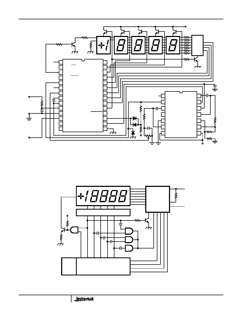
Figure 7 shows the complete circuit for a
±
4
1
/
2
digit
(
±
200mV full scale) A/D converter with LED readout using
the internal reference of the 8068A/52A. If an external
reference is used, the reference supply (pin 7) should be
connected to ground and the 300pF reference cap deleted.
The circuit also shows a typical RC input filter. Depending on
the application, the time-constant of this filter can be made
faster, slower, or the filter deleted completely. The
1
/
2
digit
LED is driven from the 7-segment decoder, with a zero
reading blanked by connecting a D
5
signal to RBI input of
the decoder.
A voltage translation network is connected between the
comparator output of the 8068A/52A and the auto-zero input
of the 71C03. The purpose of this network is to assure that,
during auto-zero, the output of the comparator is at or near the
threshold of the 71C03 logic (+2.5V) while the auto-zero
capacitor is being charged to V
REF
(+100mV for a 200mV
instrument). Otherwise, even with 0V in, some reference
integrate period would be required to drive the comparator
output to the threshold level. This would show up as an
equivalent offset error. Once the divider network has been
selected, the unit-to-unit variation should contribute less than
a tenth of a count error. A second feature is the back-to-back
diodes, used to lower the noise. In the normal operating mode
they offer a high impedance and long integrating time
constant to any noise pulses charging the auto-zero cap. At
startup or recovery from an overload, their impedance is low
to large signals so that the cap can be charged up in one
auto-zero cycle. The buffer gain does not have to be set
precisely at 10 since the gain is used in both the integrate and
deintegrate phase. For scale factors other then 200mV the
gain of the buffer should be changed to give a
±
2V buffer
output. For 2.0000V full scale this means unity gain and for
20,000mV (1
µ
V resolution) a gain of 100 is necessary. Not all
8068As can operate properly at a gain of 100 since their offset
should be less than 10mV in order to accommodate the auto-
zero circuitry. However, for devices selected with less than
10mV offset, the noise performance is reasonable with
approximately 1.5
µ
V near full scale. On all scales less than
200mV, the voltage translation network should be made
adjustable as an offset trim.
The auto-zero cap should be 1
µ
F for all scales and the
reference capacitor should be 1
µ
F times the gain of the
buffer amplifier. At this value if the input leakages of the
8052A/ 8068A are equal, the droop effects will cancel giving
zero offset. This is especially important at high temperature.
Some typical component values are shown in Table 1. For
3
1
/
2
digit conversion, use 12kHz clock.
V++ = +15V, V+ = 5V, V- = -15V
Clock Freq. = 120kHz (4
1
/
2
Digit) or 12kHz (3
1
/
2
Digit)
TABLE 1.
SPECIFICATION
VALUE
UNITS
Full Scale V
IN
20
200
2000
mV
Buffer Gain
100
(See
Note)
10
1
V/V
R
INT
100
100
100
k
C
INT
0.22
0.22
0.22
µ
F
C
AZ
1.0
1.0
1.0
µ
F
C
REF
10
10
1.0
µ
F
V
REF
10
100
1000
mV
Resolution (4
1
/
2
Digit)
1
10
100
µ
V
NOTE: Comment on offset limitations above. Buffer gain does not
improve ICL8052A noise performance adequately.
R B1
R B2
+
(
)
RB2
------------------------------------
ICL8052A/ICL71C03, ICL8068A/ICL71C03
13
FIGURE 7. ICL8052A (8068A)/71C03A 4
1
/
2
DIGIT A/D CONVERTER
V+
4
1
/
2
/ 3
1
/
2
POLARITY
RUN/HOLD
COMP IN
V-
REFERENCE
REF. CAP. 1
REF. CAP. 2
ANALOG IN
ANALOG GND
CLOCK IN
UNDER-RANGE
OVER-RANGE
BUSY
D
2
D
3
D
4
(MSB) B
8
B
2
(MSD) D
5
STROBE
A-Z IN
A-Z OUT
DIGITAL GND
(LSD) D
1
B
4
(LSB) B
1
28
27
26
25
24
23
22
21
20
19
18
17
16
15
1
2
3
4
5
6
7
8
9
10
11
12
13
14
V-
COMP OUT
REF CAP
REF BYPASS
GND
REF OUT
REF SUPPLY
INT OUT
+BUFF IN
+INT IN
-INT IN
-BUFF IN
BUFF OUT
V++
1
2
3
4
5
6
7
14
13
12
11
10
9
8
10
µ
F
-15V
10k
0.1
µ
F
+5V
SIGNAL
INPUT
CLOCK
IN
120kHz = 3
READINGS/SEC
150
150
4.7k
ICL71C03
ICL8068A
10k
90k
a
b
c
d
e
f
g
B
1
B
2
B
3
B
4
7447
RBI
+5V
47k
1
2
3
4
5
36
10
10
µ
F
300
µ
F
-15V
300
1k
+15V
100
0.22
µ
F
1.0
µ
F
-15V
150
NOTE: For 3
1
/
2
digit, tie pin 2 low and change clock to 12kHz.
k
k
k
k
FIGURE 8. ICL8052A-8068A/71C03A PLASMA DISPLAY CIRCUIT
2.5k
47k
5k
+5V
POL
a
g
HI VOLTAGE BUFFER DI 505
POL D
5
D
4
D
3
D
2
D
1
B
8
B
4
B
2
B
1
71C03A
3k
+5V
0V
0.02
µ
F
0.02
0.02
µ
F
GATES
ARE
7409
0.02
µ
F
0.02
µ
F
µ
F
8052A/
8068A
a
g
V+
PROG
A
RBI BI D
DM8880
ICL8052A/ICL71C03, ICL8068A/ICL71C03
14
A suitable circuit for driving a plasma-type display is shown
in Figure 8. The high voltage anode driver buffer is made by
Dionics. The 3 AND gates and caps driving "Bl" are needed
for interdigit blanking of multiple-digit display elements, and
can be omitted if not needed. The 2K and 3K resistors set
the current levels in the display. A similar arrangement can
be used with "Nixie
" tubes.
Nixie
is a registered trademark of Burroughs Corporation.
Analog and Digital Grounds
Extreme care must be taken to avoid ground loops in the
layout of 8068A or 8052A/71C03A circuits, especially in high
sensitivity circuits. It is most important that return currents
from digital loads are not fed into the analog ground line.
Both of the above circuits have considerable current flowing
in the digital ground returns from drivers, etc. A
recommended connection sequence for the ground lines is
shown in Figure 9.
Other Circuits for Display Applications
Popular LCD displays can be interfaced to the Output of the
ICL71C03 with suitable display drivers, such as the
ICM7211A as shown in Figure 10. A standard CMOS 4000
series LCD driver circuit is used for displaying the
1
/
2
digit,
the polarity, and the "over-range" flag. A similar circuit can be
used with the ICM7212A LED driver. Of course, another full
driver circuit could be ganged to the one shown if required.
This would be useful if additional annunciators were needed.
Figure 10 shows the complete circuit for a 4
1
/2 digit
(
±
2.000V) A/D, again using the internal reference of the
8052A/8068A.
Figure 11 shows a more complicated circuit for driving LCD
displays. Here the data is latched into the ICM7211 by the
STROBE signal and "Overrange" is indicated by blanking the
4 digits. A clock oscillator circuit using the ICM7555 CMOS
timer is shown. Some other suitable clock circuits are
suggested in Figures 12 and 13. The 2-gate circuit should
use CMOS gates to maintain good power supply rejection.
A problem sometimes encountered with the
8052A/68A/71C03 A/D is that of gross over-voltage applied
in the input. Voltage in excess of
±
2.000V may cause the
integrator output to saturate. When this occurs, the integrator
can no longer source (or sink) the current required to hold
the summing junction (Pin 11) at the voltage stored on the
auto zero capacitor. As a result, the voltage across the
integrator capacitor decreases sufficiently to give a false
voltage reading. This problem can also show up as large-
signal instability on overrange conditions. A simple solution
to this problem is to use junction FET transistors across the
integrator capacitor to source (or sink) current into the
summing junction and prevent the integrator amplifier from
saturating, as shown in Figure 14.
FIGURE 9. GROUNDING SEQUENCE
DEVICE PIN
DIG GND
ICL7104
PIN 2
DIGITAL
LOGIC
V
IN
I/P
+
-
FILTER
CAP
8068A PIN 2
COMPARATOR
PIN 11
ICL71C03
AN GND
C
AZ
V
REF
BUFF
-IN
(IF USED)
REF
VOLTAGE
BUFF
OUT
EXTERNAL
REFERENCE
(IF USED)
PIN 5
ICL8052A/68A
AN GND
+15V
-15V
+5V SUPPLY BYPASS CAPACITOR(S)
BOARD
EDGE
ANALOG SUPPLY
BYPASS CAPACITORS
ANALOG
SUPPLY
RETURN
DIGITAL
SUPPLY
RETURN
ICL8052A/ICL71C03, ICL8068A/ICL71C03
15
FIGURE 10. DRIVING LCD DISPLAYS
V+
41/2 / 31/2
POL
R/H
COMP IN
V-
REF
REF. CAP. 1
REF. CAP. 2
INPUT
ANALOG GND
CLOCK
UR
OR
BUSY
D
2
D
3
D
4
B
8
B
2
D
5
STROBE
A-Z IN
A-Z OUT
DIG GND
D
1
B
4
B
1
28
27
26
25
24
23
22
21
20
19
18
17
16
15
1
2
3
4
5
6
7
8
9
10
11
12
13
14
ICL71C03
5 BP
31 D
1
32 D
2
33 D
3
34 D
4
30 B
3
29 B
2
28 B
1
27 B
0
35 V-
37 - 40
6 - 26
2, 3, 4
OSC 36
V+ 1
+5V
BACKPLANE
28 SEGMENTS
D
1
- D
4
4
1
/
2
DIGIT LCD DISPLAY
+5V
-15V
1
µ
F
0.1
µ
F
1
2
3
4
5
6
7
14
13
12
11
10
9
8
ICL8052A
8068A
22-100pF
OPTIONAL
CAPACITOR
+5V
100k
INPUT
300
µ
F
36k
300k
-15V
-15V
1.0
µ
F
0.22
µ
F
+15V
100k
10
µ
F
5k
10k
0V
CLOCK IN (120kHz = 3 READINGS/SEC)
0V
11 10 9 2 6
13
8
7
CD4054A
14 12 5 3 4
15
16
1
+5V
0V
ANALOG GND
ICM7211A
ICL8052A/ICL71C03, ICL8068A/ICL71C03

16
FIGURE 11. 4
1
/
2
DIGIT LCD DPM WITH DIGIT BLANKING ON OVERRANGE
1
/
2
CD4030
+5V
V+
4
1
/
2
/ 3
1
/
2
POL
R/H
COMP IN
V-
REF
REF. CAP. 1
REF. CAP. 2
INPUT
ANALOG GND
CLOCK
UR
OR
BUSY
D
2
D
3
D
4
B
8
B
2
D
5
STROBE
A-Z IN
A-Z OUT
DIG GND
D
1
B
4
B
1
28
27
26
25
24
23
22
21
20
19
18
17
16
15
1
2
3
4
5
6
7
8
9
10
11
12
13
14
ICL71C03(A)
5 BP
31 D
1
32 D
2
33 D
3
34 D
4
30 B
3
29 B
2
28 B
1
27 B
0
35 V-
37 - 40
6 - 26
2, 3, 4
OSC 36
V+ 1
+5V
BACKPLANE
1
/
4
CD4030
28 SEGMENTS
D
1
- D
4
4
1
/
2
DIGIT LCD DISPLAY
CD4081
CD4071
CD4071
+5V
-15V
1
µ
F
0.1
µ
F
1
2
3
4
5
6
7
14
13
12
11
10
9
8
ICL8052A
8068A
0V
OUT
+5V
1
2
3
4
8
7
6
5
V-
V+
RESET
ICM7555
0V
+5V
4.7k
10 TO 15k
ADJUST TO
F
CL
= 120kHz
300pF
0V
22-100pF
OPTIONAL
CAPACITOR
+5V
100k
INPUT
300
µ
F
36k
300k
-15V
-15V
1.0
µ
F
0.22
µ
F
+15V
100k
10
µ
F
5k
10k
+5V
1
/
4
CD4030
ICM7211A
0V
ANALOG GND
ICL8052A/ICL71C03, ICL8068A/ICL71C03
17
Interfacing with UARTs and
Microprocessors
Figure 15 shows a very simple interface between a free-
running 8068A/8052A/71C03A and a UART. The five
STROBE pulses start the transmission of the five data words.
The digit 5 word is 0000XXXX, digit 4 is 1000XXXX, digit 3 is
0100XXXX, etc. Also, the polarity is transmitted indirectly by
using it to drive the Even Parity Enable Pin (EPE). If EPE of
the receiver is held low, a parity flag at the receiver can be
decoded as a positive signal, no flag as negative. A complex
arrangement is shown in Figure 14. Here the UART can
instruct the A/D to begin a measurement sequence by a word
on RRI. The Busy signal resets the Data Ready Reset (DRR).
Again STROBE starts the transmit sequence. A quad 2 input
multiplexer is used to superimpose polarity, over-range, and
under-range onto the D
5
word since in this instance it is
known that B
2
= B
4
= B
8
= 0.
For correct operation it is important that the UART clock be
fast enough that each word is transmitted before the next
STROBE pulse arrives. Parity is locked into the UART at
load time but does not change in this connection during an
output stream.
Circuits to interface the 71C03(A) directly with three popular
microprocessors are shown in Figures 17, 18 and 19. The
main differences in the circuits are that the IM6100 with its
12-bit word capability can accept polarity, over-range, under-
range, 4 bits of BCD and 5 digits simultaneously where the
8080/8048 and the MC6800 groups with 8-bit words need to
have polarity, over-range and under-range multiplexed onto
the Digit 5 word - as in the UART circuits. In each case the
microprocessor can instruct the A/D when to begin a
measurement and when to hold this measurement.
FIGURE 12. CMOS OSCILLATOR
FIGURE 13. LM311 OSCILLATOR
FIGURE 14. GROSS OVERVOLTAGE PROTECTION CIRCUIT
R
37.5k
f
OSC
= 0.45/RC
C
100pF
LM311
-
+
1
4
3
2
7
8
56k
1k
30k
16k
16k
390pF
+5V
0.22
µ
F
A2
+
-
A3
+
-
INTEG.
COMP.
A1
+
-
BUFFER
14
11
9
INT OUT
-INT IN
BUF OUT
10
-BUF IN
-1.2V
2
1
-15V
7
8
+15V
12
+INT IN
13
8052A/
INT.
REF.
6
3
+BUF IN
5
REF
OUT
300pF
COMP
OUT
100K
0.22
µ
F
2N5458
2N5461
S
D
S
D
8068A
REF
COMP
TO ICL71C03
Application Notes
NOTE #
DESCRIPTION
AN016
"Selecting A/D Converters"
AN017
"The Integrating A/D Converter"
AN018
"Do's and Don'ts of Applying A/D Converters"
AN023
"Low Cost Digital Panel Meter Designs"
AN028
"Build an Auto-Ranging DMM Using the 8052A / 7103A
A/D Converter Pair," by Larry Goff
ICL8052A/ICL71C03, ICL8068A/ICL71C03
18
FIGURE 15. SIMPLE ICL71C03/71C03A TO UART INTERFACE
FIGURE 16. COMPLEX ICL71C03/7103A TO UART INTERFACE
SERIAL OUTPUT
TO RECEIVING UART
TRO
UART
IM6402/3
TBR
TBRL
4
3
2
1
5
6
7
8
D
1
D
2
D
3
D
4
B
1
B
2
B
4
B
8
EPE
STROBE
RUN/HOLD
D
5
POL
71C03/A
NC
+5V
74C157
SELECT
3A
2A
1A
1B
2B
3B
D
1
D
2
D
3
D
4
B
1
B
2
B
4
B
8
STROBE
RUN/HOLD
D
5
71C03/A
+5V
ENABLE
BUSY
TRO
UART
IM6402/3
TBR
TBRL
4
3
2
1
5
6
7
8
EPE
RRI
DRR
DR
1Y
2Y
3Y
POL OVER
UNDER
10k
100pF
ICL8052A/ICL71C03, ICL8068A/ICL71C03
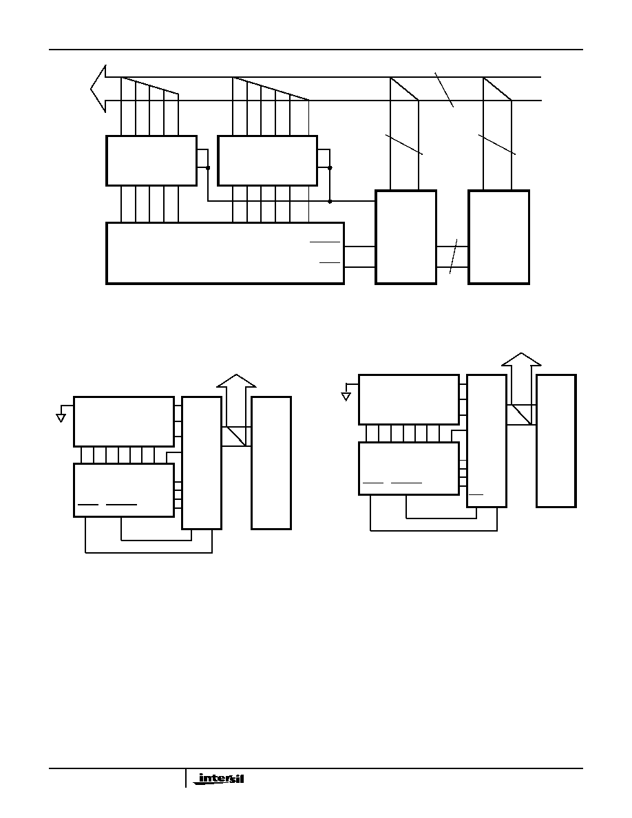
19
FIGURE 17. IM6100 TO ICL71C03A/71C03A INTERFACE
FIGURE 18. ICL71C03 TO MC6800, MCS650X INTERFACE
FIGURE 19. ICL71C03 TO MCS-48, -80, -85 INTERFACE
D
4
D
3
D
2
D
1
D
5
STROBE
RUN/HOLD
71C03/A
POL OVER
1
15
80C95
B
8
B
4
B
2
B
1
1
15
80C95
WRITE 1
SENSE 1
IM6101
READ 1
12
IM6100
12
7
12
SEL
3B
2B
1B
1A
1Y
2Y
74C157
2A 3A 3Y
EN
D
5
UNDE
R
OV
E
R
PO
L
B
8
B
1
D
1
71C03
B
4
B
2
D
4
RUN/
D
3
D
2
HOLD
STROBE
PA4
PA7
PA6
PA5
PA0
PA1
PA2
CA1 CA2
PA3
MC6820
MC680X
OR
MCS650X
SEL
3B
2B
1B
1A
1Y
2Y
74C157
2A 3A 3Y
EN
D
5
UNDE
R
OV
E
R
PO
L
B
8
B
1
D
1
71C03
B
4
B
2
D
4
RUN/
D
3
D
2
HOLD
STROBE
PA4
PA7
PA6
PA5
PA0
PA1
PA2
STB
A
PB0
PA3
8255
8080,
8085,
ETC.
(MODE 1)
ICL8052A/ICL71C03, ICL8068A/ICL71C03
20
ICL71C03 with ICL8052A/8068A Integrating A/D Converter Equations
The ICL71C03 does not have an internal crystal or RC
oscillator. It has a clock input only.
Integration Period
Integration Clock Period
t
CLOCK
= 1/f
CLOCK
60/50Hz Rejection Criterion
t
INT
/t
60Hz
or t
INT
/t
50Hz
= Integer
Optimum Integration Current
I
INT
= 20
µ
A
Full Scale Analog Input Voltage
V
INFS
(Typ) = 200mV to 2.0V = 2V
REF
Integrate Resistor
Integrate Capacitor
Integrator Output Voltage
V
INT
(Typ) = 9V
Output Count
NOTE: The 4
1
/
2
digit mode's LSD will be output as a zero in the 3
1
/
2
digit mode.
Output Type:
4 Nibbles BCD with Polarity and Over-range.
Power Supply:
±
15V, +5V
V++ = +15V
V- = -15V
V+ = +5V
V
REF
1.75V
If V
REF
not used, float output pin.
Auto Zero Capacitor Values
0.01
µ
F < C
AZ
< 1
µ
F
Reference Capacitor Value
C
REF
= (Buffer Gain) x C
AZ
t
I NT
10 000
,
f
CL OCK
---------------------
4-1/2 Digit
(
)
=
t
I NT
1 000
,
f
CL OCK
---------------------
3-1/2 Digit
(
)
=
R
I NT
BufferG ain
(
)
V
IN FS
◊
I
I NT
-------------------------------------------------------------
=
C
I NT
t
I NT
(
)
I
INT
(
)
V
INT
--------------------------------
=
V
I NT
t
INT
(
)
I
IN T
(
)
C
INT
--------------------------------
=
C ount
10 000
,
V
I N
V
REF
---------------
◊
(4-1/2 Digit)
=
C ount
1 000
,
V
IN
V
REF
---------------
◊
(3-1/2 Digit)
=
FIGURE 20. INTEGRATOR OUTPUT
AUTO ZERO
(COUNTS)
30,001 - 10,001
3,001 - 1,001
INTEGRATE
(FIXED COUNT)
10,000
1,000
DEINTEGRATE
(COUNTS)
1 - 20,001
1 - 2,001
(4
1
/
2
DIGIT)
(3
1
/
2
DIGIT)
TOTAL CONVERSION TIME (t
CONV
)
t
CONV
= 40,002 * t
CLOCK
(4
1
/
2
DIGIT MODE)
t
CONV
= 4,002 * t
CLOCK
(3
1
/
2
DIGIT MODE)
(IN CONTINUOUS MODE)
ICL8052A/ICL71C03, ICL8068A/ICL71C03

21
ICL8052A/ICL71C03, ICL8068A/ICL71C03
Dual-In-Line Plastic Packages (PDIP)
NOTES:
1. Controlling Dimensions: INCH. In case of conflict between English
and Metric dimensions, the inch dimensions control.
2. Dimensioning and tolerancing per ANSI Y14.5M-1982.
3. Symbols are defined in the "MO Series Symbol List" in Section 2.2 of
Publication No. 95.
4. Dimensions A, A1 and L are measured with the package seated in
JEDEC seating plane gauge GS-3.
5. D, D1, and E1 dimensions do not include mold flash or protrusions.
Mold flash or protrusions shall not exceed 0.010 inch (0.25mm).
6. E and
are measured with the leads constrained to be perpen-
dicular to datum
.
7. e
B
and e
C
are measured at the lead tips with the leads uncon-
strained. e
C
must be zero or greater.
8. B1 maximum dimensions do not include dambar protrusions. Dambar
protrusions shall not exceed 0.010 inch (0.25mm).
9. N is the maximum number of terminal positions.
10. Corner leads (1, N, N/2 and N/2 + 1) for E8.3, E16.3, E18.3, E28.3,
E42.6 will have a B1 dimension of 0.030 - 0.045 inch (0.76 -
1.14mm).
e
A
-C-
C
L
E
e
A
C
e
B
e
C
-B-
E1
INDEX
1 2 3
N/2
N
AREA
SEATING
BASE
PLANE
PLANE
-C-
D1
B1
B
e
D
D1
A
A2
L
A1
-A-
0.010 (0.25)
C
A
M
B S
E14.3
(JEDEC MS-001-AA ISSUE D)
14 LEAD DUAL-IN-LINE PLASTIC PACKAGE
SYMBOL
INCHES
MILLIMETERS
NOTES
MIN
MAX
MIN
MAX
A
-
0.210
-
5.33
4
A1
0.015
-
0.39
-
4
A2
0.115
0.195
2.93
4.95
-
B
0.014
0.022
0.356
0.558
-
B1
0.045
0.070
1.15
1.77
8
C
0.008
0.014
0.204
0.355
-
D
0.735
0.775
18.66
19.68
5
D1
0.005
-
0.13
-
5
E
0.300
0.325
7.62
8.25
6
E1
0.240
0.280
6.10
7.11
5
e
0.100 BSC
2.54 BSC
-
e
A
0.300 BSC
7.62 BSC
6
e
B
-
0.430
-
10.92
7
L
0.115
0.150
2.93
3.81
4
N
14
14
9
Rev. 0 12/93
22
ICL8052A/ICL71C03, ICL8068A/ICL71C03
Dual-In-Line Plastic Packages (PDIP)
NOTES:
1. Controlling Dimensions: INCH. In case of conflict between English and
Metric dimensions, the inch dimensions control.
2. Dimensioning and tolerancing per ANSI Y14.5M-1982.
3. Symbols are defined in the "MO Series Symbol List" in Section 2.2 of
Publication No. 95.
4. Dimensions A, A1 and L are measured with the package seated in
JEDEC seating plane gauge GS-3.
5. D, D1, and E1 dimensions do not include mold flash or protrusions.
Mold flash or protrusions shall not exceed 0.010 inch (0.25mm).
6. E and
are measured with the leads constrained to be perpendic-
ular to datum
.
7. e
B
and e
C
are measured at the lead tips with the leads unconstrained.
e
C
must be zero or greater.
8. B1 maximum dimensions do not include dambar protrusions. Dambar
protrusions shall not exceed 0.010 inch (0.25mm).
9. N is the maximum number of terminal positions.
10. Corner leads (1, N, N/2 and N/2 + 1) for E8.3, E16.3, E18.3, E28.3,
E42.6 will have a B1 dimension of 0.030 - 0.045 inch (0.76 - 1.14mm).
e
A
-C-
C
L
E
e
A
C
e
B
e
C
-B-
E1
INDEX
1 2 3
N/2
N
AREA
SEATING
BASE
PLANE
PLANE
-C-
D1
B1
B
e
D
D1
A
A2
L
A1
-A-
0.010 (0.25)
C
A
M
B S
E28.6
(JEDEC MS-011-AB ISSUE B)
28 LEAD DUAL-IN-LINE PLASTIC PACKAGE
SYMBOL
INCHES
MILLIMETERS
NOTES
MIN
MAX
MIN
MAX
A
-
0.250
-
6.35
4
A1
0.015
-
0.39
-
4
A2
0.125
0.195
3.18
4.95
-
B
0.014
0.022
0.356
0.558
-
B1
0.030
0.070
0.77
1.77
8
C
0.008
0.015
0.204
0.381
-
D
1.380
1.565
35.1
39.7
5
D1
0.005
-
0.13
-
5
E
0.600
0.625
15.24
15.87
6
E1
0.485
0.580
12.32
14.73
5
e
0.100 BSC
2.54 BSC
-
e
A
0.600 BSC
15.24 BSC
6
e
B
-
0.700
-
17.78
7
L
0.115
0.200
2.93
5.08
4
N
28
28
9
Rev. 1 12/00

23
All Intersil products are manufactured, assembled and tested utilizing ISO9000 quality systems.
Intersil Corporation's quality certifications can be viewed at website www.intersil.com/design/quality/iso.asp.
Intersil products are sold by description only. Intersil Corporation reserves the right to make changes in circuit design and/or specifications at any time without notice.
Accordingly, the reader is cautioned to verify that data sheets are current before placing orders. Information furnished by Intersil is believed to be accurate and reliable. How-
ever, no responsibility is assumed by Intersil or its subsidiaries for its use; nor for any infringements of patents or other rights of third parties which may result from its use.
No license is granted by implication or otherwise under any patent or patent rights of Intersil or its subsidiaries.
For information regarding Intersil Corporation and its products, see web site www.intersil.com
Sales Office Headquarters
NORTH AMERICA
Intersil Corporation
2401 Palm Bay Rd.
Palm Bay, FL 32905
TEL: (321) 724-7000
FAX: (321) 724-7240
EUROPE
Intersil SA
Mercure Center
100, Rue de la Fusee
1130 Brussels, Belgium
TEL: (32) 2.724.2111
FAX: (32) 2.724.22.05
ASIA
Intersil Ltd.
8F-2, 96, Sec. 1, Chien-kuo North,
Taipei, Taiwan 104
Republic of China
TEL: 886-2-2515-8508
FAX: 886-2-2515-8369
ICL8052A/ICL71C03, ICL8068A/ICL71C03
Ceramic Dual-In-Line Frit Seal Packages (CERDIP)
NOTES:
1. Index area: A notch or a pin one identification mark shall be locat-
ed adjacent to pin one and shall be located within the shaded
area shown. The manufacturer's identification shall not be used
as a pin one identification mark.
2. The maximum limits of lead dimensions b and c or M shall be
measured at the centroid of the finished lead surfaces, when
solder dip or tin plate lead finish is applied.
3. Dimensions b1 and c1 apply to lead base metal only. Dimension
M applies to lead plating and finish thickness.
4. Corner leads (1, N, N/2, and N/2+1) may be configured with a
partial lead paddle. For this configuration dimension b3 replaces
dimension b2.
5. This dimension allows for off-center lid, meniscus, and glass
overrun.
6. Dimension Q shall be measured from the seating plane to the
base plane.
7. Measure dimension S1 at all four corners.
8. N is the maximum number of terminal positions.
9. Dimensioning and tolerancing per ANSI Y14.5M - 1982.
10. Controlling dimension: INCH.
bbb
C A - B
S
c
Q
L
A
SEATING
BASE
D
PLANE
PLANE
-D-
-A-
-C-
-B-
D
E
S1
b2
b
A
e
M
c1
b1
(c)
(b)
SECTION A-A
BASE
LEAD FINISH
METAL
e
A/2
A
M
S
S
ccc
C A - B
M
D
S
S
aaa
C A - B
M
D
S
S
e
A
F14.3
MIL-STD-1835 GDIP1-T14 (D-1, CONFIGURATION A)
14 LEAD CERAMIC DUAL-IN-LINE FRIT SEAL PACKAGE
SYMBOL
INCHES
MILLIMETERS
NOTES
MIN
MAX
MIN
MAX
A
-
0.200
-
5.08
-
b
0.014
0.026
0.36
0.66
2
b1
0.014
0.023
0.36
0.58
3
b2
0.045
0.065
1.14
1.65
-
b3
0.023
0.045
0.58
1.14
4
c
0.008
0.018
0.20
0.46
2
c1
0.008
0.015
0.20
0.38
3
D
-
0.785
-
19.94
5
E
0.220
0.310
5.59
7.87
5
e
0.100 BSC
2.54 BSC
-
eA
0.300 BSC
7.62 BSC
-
eA/2
0.150 BSC
3.81 BSC
-
L
0.125
0.200
3.18
5.08
-
Q
0.015
0.060
0.38
1.52
6
S1
0.005
-
0.13
-
7
90
o
105
o
90
o
105
o
-
aaa
-
0.015
-
0.38
-
bbb
-
0.030
-
0.76
-
ccc
-
0.010
-
0.25
-
M
-
0.0015
-
0.038
2, 3
N
14
14
8
Rev. 0 4/94