
5-6
Features
∑ 16-Bit/14-Bit Binary Three-State Latched Outputs Plus
Polarity and Overrange
∑ Ideally Suited for Interface to UARTs and
Microprocessors
∑ Conversion on Demand or Continuously
∑ Guaranteed Zero Reading for 0V Input
∑ True Polarity at Zero Count for Precise Null Detection
∑ Single Reference Voltage for True Ratiometric
Operation
∑ Onboard Clock and Reference
∑ Auto-Zero, Auto-Polarity
∑ Accuracy Guaranteed to 1 Count
∑ All Outputs TTL Compatible
∑
±
4V Analog Input Range
∑ Status Signal Available for External Sync, A/Z in
Preamp, Etc.
Description
The ICL7104, combined with the ICL8052 or ICL8068,
forms a member of Intersil' high performance A/D converter
family. The ICL7104-16, performs the analog switching and
digital function for a 16-bit binary A/D converter, with full
three-state output, UART handshake capability, and other
outputs for easy interfacing. The ICL7014-14 is a 14-bit
version. The analog section, as with all Intersil' integrating
converters, provides fully precise Auto-Zero, Auto-Polarity
(including
±
0 null indication), single reference operation,
very high input impedance, true input integration over a
constant period for maximum EMI rejection, fully
rationmetric operation, over-range indication, and a
medium quality built-in reference. The chip pair also offers
optional input buffer gain for high sensitivity applications, a
built-in clock oscillator, and output signals for providing an
external Auto-Zero capability in preconditioning circuitry,
synchronizing external multiplexers, etc.
Ordering Information
PART NUMBER
TEMP.
RANGE (
o
C)
PACKAGE
PKG.
NO.
ICL8052CPD
0 to 70
14 Ld PDIP
E14.3
lCL8052CDD
0 to 70
14 Ld CERDIP
F14.3
lCL8052ACPD
0 to 70
14 Ld PDIP
E14.3
ICL8052ACDD
0 to 70
14 Ld CERDIP
F14.3
ICL8068CDD
0 to 70
14 Ld CERDIP
F14.3
ICL8068ACDD
0 to 70
14 Ld CERDIP
F14.3
lCL8068ACJD
0 to 70
14 Ld CERDIP
F14.3
ICL7104-14CPL
0 to 70
40 Ld PDIP
E40.6
lCL7104-16CPL
0 to 70
40 Ld PDIP
E40.6
August 1997
ICL8052/ICL7104,
ICL8068/ICL7104
14-Bit/16-Bit, Microprocessor-
Compatible, 2-Chip, A/D Converter
File Number
3091.1
CAUTION: These devices are sensitive to electrostatic discharge; follow proper IC Handling Procedures.
1-888-INTERSIL or 321-724-7143 | Copyright © Intersil Corporation 1999
5-7
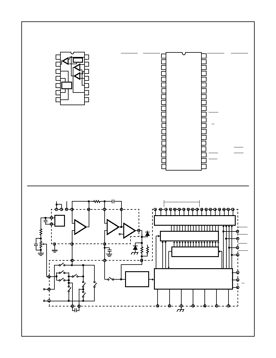
Pinouts
Functional Block Diagram
ICL8052/ICL8068
(CERDIP, PDIP)
TOP VIEW
ICL7104
(PDIP)
TOP VIEW
V-
COMP OUT
REF CAP
REF BYPASS
GND
REF OUT
REF SUPPLY
INT OUT
+BUFF IN
+INT IN
-INT IN
-BUFF IN
BUFF OUT
V++
1
2
3
4
5
6
7
14
13
12
11
10
9
8
-1.2V
V
REF
ICL8052/
ICL8068
(OUTLINE DWGS DD, JD, PD)
13
1
2
3
4
5
6
7
8
9
10
11
12
14
15
16
17
18
19
20
V++
DIG GND
STTS
POL
OR
BIT 14
BIT 13
BIT 12
BIT 11
BIT 10
BIT 9
NC
NC
BIT 8
BIT 7
BIT 6
BIT 5
BIT 4
BIT 3
BIT 2
28
40
39
38
37
36
35
34
33
32
31
30
29
27
26
25
24
23
22
21
V-
COMP IN
REFCAP 1
V
REF
AZ
ANALOG
REFCAP 2
BUF IN
ANALOG I/P
V+
CE/LD
SEN
R/H
MODE
CLK 2
CLK 1
CLK 3
HBEN
LBEN
BIT 1
ICL7104-14
GND
V++
DIG GND
STTS
POL
OR
BIT 16
BIT 15
BIT 14
BIT 13
BIT 12
BIT 11
BIT 10
BIT 9
BIT 8
BIT 7
BIT 6
BIT 5
BIT 4
BIT 3
BIT 2
ICL7104-14
ICL7104-16
ICL7104-14
ICL7104-16
HBEN
MBEN
(OUTLINE DWGS DL,
JL, PL)
FIGURE 1. ICL8052A (8068A)/ICL7104 16-BIT/14-BIT A/D CONVERTER FUNCTIONAL DIAGRAM
A2
+
-
A3
+
-
INTEG.
COMP.
A1
+
-
BUFFER
14
11
9
INT OUT
-INT IN
BUF OUT
10
-BUF IN
-1.2V
2
50k
-15V
+5V
R
INT
C
INT
1
-15V
7
8
+15V
C
AZ
12
+INT IN
13
8052/8068
INT.
REF.
6
3
+BUF IN
5
REF
OUT
5k
10k
300pF
10
µ
F
COMP
OUT
COMP IN
300k
39
36
33
8 9
6 7
12 13
10 11
16 17
14 15
20 21
18 19
5
4
14 13
16 15
10 9
12 11
6 5
8
7
2 1
4 3
OR POL
THREE-STATE OUTPUTS
LATCHES
COUNTER
24 HBEN
23 MBEN
22 LBEN
30 CE/LD
CONTROL LOGIC
ZERO
CROSSING
DETECTOR
29
27
28
7104
+BUF IN
AZ
SW3
SW5
SW4
SW6
SW8
SW2
SW9
SW7
SW1
34
REF CAP (2)
REF CAP (1)
38
C
REF
37
32
35
ANALOG
GND
ANALOG
INPUT
V
REF
SEN
MODE
R/H
BITS
3
STTS
26
CLOCK
25
CLOCK
40
-15V
2
1
+15V
31
+5V
(2)
(1)
ICL8052/ICL7104, ICL8068/ICL7104

5-8
Pin Descriptions
PIN NO.
SYMBOL
OPTION
DESCRIPTION
1
V++
Positive Supply Voltage: Nominally +15V.
2
GND
Digital Ground: 0V, ground return.
3
STTS
Status Output: HI during integrate and deintegrate until data is latched. LO when analog section
is in auto-zero configuration.
4
POL
Polarity: Three-state output. HI for positive input.
5
OR
Over Range: Three-state output.
6
BIT 16
BIT 14
-16
-14
Most Significant Bit (MSB).
7
BIT 15
BIT 13
-16
-14
DATA Bits: Three-state outputs. See Table 3 for format of ENABLES and bytes. HIGH = true.
8
BIT 14
BIT 12
-16
-14
9
BIT 13
BIT 11
-16
-14
10
BIT 12
BIT 10
-16
-14
11
BIT 11
BIT 9
-16
-14
12
BIT 10
NC
-16
-14
13
BIT 9
NC
-16
-14
14
BIT 8
15
BIT 7
16
BIT 6
17
BIT 5
18
BIT 4
19
BIT 3
20
BIT 2
21
BIT 1
Least Significant Bit (LSB).
22
LBEN
LOW BYTE ENABLE: If not in handshake mode (see pin 27) when LO (with CE/LD, pin 30)
activates low-order byte outputs, BITS 1-8. When in handshake mode (see pin 27), serves as a
low byte flag output. See Figures 11, 12, 13.
23
MBEN
-16
MID BYTE ENABLE: Activates Bits 9-16, see LBEN (pin 22)
HBEN
-14
HIGH BYTE ENABLE: Activates Bits 9-14, POL, OR, see LBEN (pin 22)
24
HBEN
-16
HIGH BYTE ENABLE: Activates POL, OR, see LBEN (pin 22).
CLOCK3
-14
RC oscillator pin: Can be used as clock output.
ICL8052/ICL7104, ICL8068/ICL7104

5-9
25
CLOCK 1
Clock Input: External clock or ocsillator.
26
CLOCK 2
Clock Output: Crystal or RC oscillator.
27
MODE
INPUT LO: Direct output mode where CE/LD, HBEN, MBEN and LBEN act as inputs directly
controlling byte outputs. If pulsed HI causes immediate entry into handshake mode (see Figure
13). If HI, enables CE/LD, HBEN, MBEN and LBEN as outputs. Handshake mode will be entered
and data output as in Figures 11 and 12 at conversion completion.
28
R/H
RUN/HOLD: Input HI conversions continuously performed every 2
17
(-16) or 2
15
(-14) clock
pulses. Input LO conversion in progress completed, converter will stop in Auto-Zero 7 counts
before input integrate.
29
SEN
SEND ENABLE: Input controls timing of byte transmission in handshake mode. HI indicates
`send'.
30
CE/LD
CHIP ENABLE/ LOAD: WITH MODE (PIN 27) LO, CE/LD serves as a master output enable;
when HI, the bit outputs and POL, OR are disabled. With MODE HI, pin serves as a LOAD strobe
(-ve going) used in handshake mode. See Figures 11 and 12.
31
V+
Positive Logic Supply Voltage: Nominally +5V.
32
AN I/P
Analog Input: High Side.
33
BUF IN
Buffer Input: Buffer Analog to analog chip (ICL8052 or ICL8086).
34
REFCAP2
Reference Capacitor: Negative Side.
35
AN. GND
Analog Ground: Input low side and reference low side.
36
A-Z
Auto-Zero node.
37
V
REF
Voltage Reference: Input (positive side).
38
REFCAP1
Reference Capacitor: Positive side.
39
COMP-IN
Comparator Input: From 8052/8068.
40
V-
Negative Supply Voltage: Nominally -15V.
Pin Descriptions
(Continued)
PIN NO.
SYMBOL
OPTION
DESCRIPTION
ICL8052/ICL7104, ICL8068/ICL7104

5-10
Absolute Maximum Ratings
Thermal Information
ICL8052, ICL8068
Supply Voltage . . . . . . . . . . . . . . . . . . . . . . . . . . . . . . . . . . . . .
±
18V
Differential Input Voltage
(8068) . . . . . . . . . . . . . . . . . . . . . . . . . . . . . . . . . . . . . . . . . .
±
30V
(8052) . . . . . . . . . . . . . . . . . . . . . . . . . . . . . . . . . . . . . . . . . . .
±
6V
Input Voltage (Note 2). . . . . . . . . . . . . . . . . . . . . . . . . . . . . . . .
±
15V
Output Short Circuit Duration All Outputs (Note 3). . . . . . . Indefinite
ICL7104
V+ Supply (GND to V+) . . . . . . . . . . . . . . . . . . . . . . . . . . . . . . . 12V
V++ to V-. . . . . . . . . . . . . . . . . . . . . . . . . . . . . . . . . . . . . . . . . . . 32V
Positive Supply Voltage (GND to V++) . . . . . . . . . . . . . . . . . . . . 17V
Negative Supply Voltage (GND to V-). . . . . . . . . . . . . . . . . . . . .-17V
Analog Input Voltage (Pins 32 - 39)(Note 4). . . . . . . . . . . . V++ to V-
Digital Input Voltage
(Pins 2 - 30) (Note 5) . . . . . . . . . . . . (GND - 0.3V) to (V+ + 0.3V)
Operating Conditions
Temperature Range . . . . . . . . . . . . . . . . . . . . . . . . . . . .0
o
C to 70
o
C
Thermal Resistance (Typical, Note 1)
JA
(
o
C/W)
JC
(
o
C/W)
14 Ld PDIP Package . . . . . . . . . . . . . .
100
N/A
40 Ld PDIP Package . . . . . . . . . . . . . .
60
N/A
14 Ld CERDIP Package . . . . . . . . . . .
75
20
Maximum Junction Temperature (Ceramic Package) . . . . . . . . . 175
o
C
Maximum Junction Temperature (Plastic Package) . . . . . . . . 150
o
C
Maximum Storage Temperature Range . . . . . . . . . .-65
o
C to 150
o
C
Maximum Lead Temperature (Soldering, 10s) . . . . . . . . . . . . 300
o
C
CAUTION: Stresses above those listed in "Absolute Maximum Ratings" may cause permanent damage to the device. This is a stress only rating and operation
of the device at these or any other conditions above those indicated in the operational sections of this specification is not implied.
NOTES:
1.
JA
is measured with the component mounted on an evaluation PC board in free air.
2. For supply voltages less than
±
15V, the absolute maximum input voltage is equal to the supply voltage.
3. Short circuit may be to ground or either supply. Rating applies to 70
o
C ambient temperature.
4. Input voltages may exceed the supply voltages provided the input current is limited to
±
100
µ
A.
5. Connecting any digital inputs or outputs to voltages greater than V+ or less than GND may cause destructive device latchup. For this
reason it is recommended that the power supply to the ICL7104 be established before any inputs from sources not on that supply are
applied.
ICL7104 Electrical Specifications
V+ = +5V, V++ = +15V, V- = -15V, T
A
= 25
o
C, f
CLOCK
= 200kHz
PARAMETER
SYMBOL
TEST
CONDITIONS
MIN
TYP
MAX
UNITS
Clock Input, CLK 1
I
IN
V
IN
= +5V to 0V
±
2
±
7
±
30
µ
A
Comparator I/P, COMP IN (Note 6)
I
IN
V
IN
= 0V to +5V
-10
±
0.001
10
µ
A
Inputs with Pulldown, MODE
I
IH
V
IN
= +5V
1
5
30
µ
A
I
IL
V
IN
= 0V
-10
±
0.01
10
µ
A
Inputs with Pullups
SEN, R/H
LBEN, MBEN, HBEN, CE/LD (Note 7)
I
IH
V
IN
= +5V
-10
±
0.01
10
µ
A
I
IL
V
IN
= 0V
-30
-5
-1
µ
A
Input High Voltage, All Digital Inputs
V
IH
2.5
2.0
-
V
Input Low Voltage, All Digital Inputs
V
IL
-
1.5
1.0
V
Digital Outputs Three-Stated On,
LBEN, MBEN (16 Only), HBEN, CE/LD
BIT n, POL, OR (Note 8)
V
OL
I
OL
= 1.6mA
-
0.27
0.4
V
V
OH
I
OH
= -10
µ
A
-
4.5
-
V
V
OH
I
OH
= -240
µ
A
2.4
3.5
-
V
Digital Outputs Three-Stated Off
Bit n, POL, OR
I
OL
0
V
OUT
V+
-10
±
0.001
+10
µ
A
Non Three-State Digital Output
STTS
V
OL
I
OL
= 3.2mA
-
0.3
0.4
V
V
OH
I
OH
= -400
µ
A
2.4
3.3
-
V
Clock 2
V
OL
I
OL
= 320
µ
A
-
0.5
-
V
V
OH
I
OH
= -320
µ
A
-
4.5
-
V
Clock 3 (-14 Only)
V
OL
I
OL
= 1.6mA
-
0.27
0.4
V
V
OH
I
OH
= -320
µ
A
2.4
3.5
-
V
ICL8052/ICL7104, ICL8068/ICL7104

5-11
Switch
Switch 1
r
DS(ON)
-
25k
-
Switches 2, 3
r
DS(ON)
-
4k
20k
Switches 4, 5, 6, 7, 8, 9
r
DS(ON)
-
2k
10k
Switch Leakage
I
D(OFF)
-
15
-
pA
Clock Frequency (Note 9)
f
CLOCK
DC
200
400
kHz
Supply Currents
+5V Supply Current
All outputs high impedance
I+
Frequency = 200kHz
-
200
600
µ
A
+5V Supply Current
I++
Frequency = 200kHz
-
0.3
1.0
mA
-5V Supply Current
I-
Frequency = 200kHz
-
25
200
µ
A
Supply Voltage Range
Logic Supply
V+
Note 10
4
-
11
V
Positive Supply
V++
10
-
16
V
Negative Supply
V-
-16
-
-10
V
NOTES:
6. This specification applies when not in Auto-Zero phase.
7. Apply only when these pins are inputs, i.e., the mode pin is low, and the 7104 is not in handshake mode.
8. Apply only when these pins are outputs, i.e., the mode pin is high, or the 7104 is in handshake mode.
9. Clock circuit shown in Figures 14 and 15.
10. V+ must not be more positive than V++.
ICL8068 Electrical Specifications
V
SUPPLY
=
±
15V, Unless Otherwise Specified
PARAMETER
SYMBOL
TEST
CONDITIONS
ICL8068
ICL8068A
UNITS
MIN
TYP
MAX
MIN
TYP
MAX
EACH OPERATIONAL AMPLIFIER
Input Offset Voltage
V
OS
V
CM
= 0V
-
20
65
-
20
65
mV
Input Current (Either Input) (Note 11)
I
IN
V
CM
= 0V
-
175
250
-
80
150
pA
Common-Mode Rejection Ratio
CMRR
V
CM
=
±
10V
70
90
-
70
90
-
dB
Non-Linear Component of Common-
Mode Rejection Ratio (Note 12)
V
CM
=
±
2V
-
110
-
-
110
-
dB
Large Signal Voltage Gain
A
V
R
L
= 50k
20,000
-
-
20,000
-
-
V/V
Slew Rate
SR
-
6
-
-
6
-
V/
µ
s
Unity Gain Bandwidth
GBW
-
2
-
-
2
-
MHz
Output Short-Circuit Current
I
SC
-
5
-
-
5
-
mA
COMPARATOR AMPLIFIER
Small-Signal Voltage Gain
A
VOL
R
L
= 30k
-
4000
-
-
-
-
V/V
Positive Output Voltage Swing
+V
O
12
13
-
12
13
-
V
Negative Output Voltage Swing
-V
O
-2.0
-2.6
-
-2.0
-2.6
-
V
VOLTAGE REFERENCE
Output Voltage
V
O
1.5
1.75
2.0
1.60
1.75
1.90
V
Output Resistance
R
O
-
5
-
-
5
-
ICL7104 Electrical Specifications
V+ = +5V, V++ = +15V, V- = -15V, T
A
= 25
o
C, f
CLOCK
= 200kHz (Continued)
PARAMETER
SYMBOL
TEST
CONDITIONS
MIN
TYP
MAX
UNITS
ICL8052/ICL7104, ICL8068/ICL7104

5-12
Temperature Coefficient
TC
-
50
-
-
40
-
ppm/
o
C
Supply Voltage Range
V
SUPPLY
±
10
-
±
16
±
10
-
±
16
V
Supply Current Total
I
SUPPLY
-
-
14
-
8
14
mA
ICL8052 Electrical Specifications
V
SUPPLY
=
±
15V, Unless Otherwise Specified
PARAMETER
SYMBOL
TEST
CONDITIONS
ICL8052
ICL8052A
UNITS
MIN
TYP
MAX
MIN
TYP
MAX
EACH OPERATIONAL AMPLIFIER
Input Offset Voltage
V
OS
V
CM
= 0V
-
20
75
-
20
75
mV
Input Current (Either Input) (Note 11)
I
IN
V
CM
= 0V
-
5
50
-
2
10
pA
Common-Mode Rejection Ratio
CMRR
V
CM
=
±
10V
70
90
-
70
90
-
dB
Non-Linear Component of Common-
Mode Rejection Ratio (Note 12)
V
CM
=
±
2V
-
110
-
-
110
-
dB
Large Signal Voltage Gain
A
V
R
L
= 50k
20,000
-
-
20,000
-
-
V/V
Slew Rate
SR
-
6
-
-
6
-
V/
µ
s
Unity Gain Bandwidth
GBW
-
1
-
-
1
-
MHz
Output Short-Circuit Current
I
SC
-
20
-
-
20
-
mA
COMPARATOR AMPLIFIER
Small-Signal Voltage Gain
A
VOL
R
L
= 30k
-
4000
-
-
-
-
V/V
Positive Output Voltage Swing
+V
O
12
13
-
12
13
-
V
Negative Output Voltage Swing
-V
O
-2.0
-2.6
-
-2.0
-2.6
-
V
VOLTAGE REFERENCE
Output Voltage
V
O
1.5
1.75
2.0
1.60
1.75
1.90
V
Output Resistance
R
O
-
5
-
-
5
-
Temperature Coefficient
TC
-
50
-
-
40
-
ppm/
o
C
Supply Voltage Range
V
SUPPLY
±
10
-
±
16
±
10
-
±
16
V
Supply Current Total
I
SUPPLY
-
6
12
-
6
12
mA
NOTES:
11. The input bias currents are junction leakage currents which approximately double for every 10
o
C increase in the junction temperature,
T
J
. Due to limited production test time, the input bias currents are measured with junctions at ambient temperature. In normal operation
the junction temperature rises above the ambient temperature as a result of internal power dissipation, P
D
. T
J
= T
A
+ R
JA
P
D
where
R
JA
is the thermal resistance from junction to ambient. A heat sink can be used to reduce temperature rise.
12. This is the only component that causes error in dual-slope converter.
ICL8068 Electrical Specifications
V
SUPPLY
=
±
15V, Unless Otherwise Specified (Continued)
PARAMETER
SYMBOL
TEST
CONDITIONS
ICL8068
ICL8068A
UNITS
MIN
TYP
MAX
MIN
TYP
MAX
ICL8052/ICL7104, ICL8068/ICL7104

5-13
System Electrical Specifications: ICL8068/ICL7104
V++ = +15V, V+ = +5V, V- = -15V, f
CLOCK
= 200kHz (Note 16)
PARAMETER
TEST
CONDITIONS
ICL8068A/ICL7104-14
ICL8068A/ICL7104-16
UNITS
MIN
TYP
MAX
MIN
TYP
MAX
Zero Input Reading
V
IN
= 0V, V
REF
= 2V
-00000
±
00000
+00000
-00000
±
00000
+00000
Counts
Ratiometric Error (Note 13)
V
IN
= V
REF
= 2V
-1
0
1
-1
0
1
LSB
Linearity Over
±
Full Scale (Error of
Reading from Best Straight Line)
-4V
V
IN
+4V
-
0.5
1
-
0.5
1
LSB
Differential Linearity (Difference
between Worst Case Step of Adjacent
Counts and Ideal Step)
-4V
V
IN
+4V
-
0.01
-
-
0.01
-
LSB
Rollover Error (Difference in Reading
for Equal Positive & Negative Voltage
Near Full Scale)
-V
IN
= +V
IN
4V
-
0.5
1
-
0.5
1
LSB
Noise (P-P Value Not Exceeded 95%
of Time)
V
IN
= 0V,
Full Scale = 4V
-
2
-
-
2
-
µ
V
Leakage Current at Input (Note 14)
V
IN
= 0V
-
100
165
-
100
165
pA
Zero Reading Drift
V
IN
= 0V,
0
o
C to 70
o
C
-
0.5
-
-
0.5
-
µ
V/
o
C
Scale Factor Temperature Coefficient
(Note 15)
V
IN
= 4V,
0
o
C to 50
o
C
ext. ref. 0ppm/
o
C
-
2
5
-
2
5
ppm/
o
C
System Electrical Specifications: ICL8052/ICL7104
V++ = +15V, V+ = +5V, V- = -15V, f
CLOCK
= 200kHz (Note 16)
PARAMETER
TEST
CONDITIONS
ICL8052A/ICL7104-14
ICL8052A/ICL7104-16
UNITS
MIN
TYP
MAX
MIN
TYP
MAX
Zero Input Reading
V
IN
= 0V, V
REF
= 2V
-00000
±
00000
+00000
-00000
±
00000
+00000
Counts
Ratiometric Error (Note 15)
V
IN
= V
REF
= 2V
-1
0
1
-1
0
1
LSB
Linearity Over
±
Full Scale (Error of
Reading from Best Straight Line)
-4V
V
IN
+4V
-
0.5
1
-
0.5
1
LSB
Differential Linearity (Difference
between Worst Case Step of Adjacent
Counts and Ideal Step)
-4V
V
IN
+4V
-
0.01
-
-
0.01
-
LSB
Rollover Error (Difference in Reading
for Equal Positive and Negative
Voltage Near Full Scale)
-V
IN
= +V
IN
4V
-
0.5
1
-
0.5
1
LSB
Noise (Peak-to-Peak Value Not
Exceeded 95% of Time)
V
IN
= 0V,
Full Scale = 4V
-
30
-
-
30
-
µ
V
Leakage Current at Input (Note 14)
V
IN
= 0V
-
20
30
-
20
30
pA
Zero Reading Drift
V
IN
= 0V,
0
o
C to 70
o
C
-
0.5
-
-
0.5
-
µ
V/
o
C
Scale Factor Temperature Coefficient
V
IN
= 4V,
0
o
C to 50
o
C
ext. ref. 0ppm/
o
C
-
2
-
-
2
-
ppm/
o
C
NOTES:
13. Tested with low dielectric absorption integrating capacitor.
14. The input bias currents are junction leakage currents which approximately double for every 10
o
C increase in the junction temperature,
T
J
. Due to limited production test time, the input bias currents are measured with junctions at ambient temperature. In normal oper-
ation the junction temperature rises above the ambient temperature as a result of internal power dissipation, P
D
. T
J
= T
A
+ R
JA
P
D
where R
JA
is the thermal resistance from junction to ambient. A heat sink can be used to reduce temperature rise.
15. The temperature range can be extended to 70
o
C and beyond if the Auto-Zero and Reference capacitors are increased to absorb the
high temperature leakage of the 8068. See note 14 above.
16. System Electrical Specifications are not tested; for reference only.
ICL8052/ICL7104, ICL8068/ICL7104

5-14
FIGURE 2. FULL 18-BIT THREE-STATE OUTPUT
CE/LD HBEN MBEN LBEN
R/H
OR
POL
MSB
LSB
MODE
8052A/
8068A
7104 -16
OR CHIP SELECT 2
CHIP SELECT 1
CONVERT
CONTROL
18
18
FIGURE 3. VARIOUS COMBINATIONS OF BYTE DISABLES
CE/LD
HBEN MBEN LBEN
R/H
OR
POL
MSB
LSB
MODE
8052A/
8068A
7104
CONVERT
2
CONTROL
CE/LD
HBEN MBEN LBEN
R/H
OR
POL
MSB
LSB
MODE
8052A/
8068A
7104
CONVERT
CONTROL
CE/LD
HBEN MBEN LBEN
R/H
OR
POL
MSB
LSB
MODE
8052A/
8068A
7104
CONVERT
CONTROL
8
8
2
16
10
8
FIGURE 4. DIRECT MODE TIMING DIAGRAM
DATA
VALID
DATA
VALID
DATA
VALID
DATA
VALID
DATA
VALID
CE/LD
AS INPUT
HBEN
AS INPUT
MBEN
AS INPUT
LBEN
AS INPUT
HIGH BYTE
DATA
BYTE
ENABLE
LOW BYTE
ENABLE
MIDDLE
t
BEA
t
DAB
t
DHB
t
DAC
t
DHC
t
CEA
= HIGH IMPEDANCE
ICL8052/ICL7104, ICL8068/ICL7104
5-15
TABLE 1. DIRECT MODE TIMING REQUIREMENTS (Note: Not tested in production)
SYMBOL
DESCRIPTION
MIN
TYP
MAX
UNIT
t
BEA
XBEN (Min) Pulse Width.
-
300
-
ns
t
DAB
Data Access Time from XBEN.
-
300
-
ns
t
DHB
Data Hold Time from XBEN.
-
200
-
ns
t
CEA
CE/LD Min. Pulse Width.
-
350
-
ns
t
DAC
Data Access Time from CE/LD.
-
350
-
ns
t
DHC
Data Hold Time from CE/LD.
-
280
-
ns
t
CWH
CLOCK 1 High Time.
-
1000
-
ns
TABLE 2. HANDSHAKE TIMING REQUIREMENTS (Note: Not tested in production)
SYMBOL
DESCRIPTION
MIN
TYP
MAX
UNIT
t
MW
Mode Pulse (Min).
-
20
-
ns
t
SM
Mode Pin Set-Up Time.
-
-150
-
ns
t
ME
Mode Pin High to Low Z CE/LD High Delay.
-
200
-
ns
t
MB
Mode Pin High to XBEN Low Z (High) Delay.
-
200
-
ns
t
CEL
Clock 1 High to CE/LD Low Delay.
-
700
-
ns
t
CEH
Clock 1 High to CE/LD High Delay.
-
600
-
ns
t
CBL
Clock 1 High to XBEN Low Delay.
-
900
-
ns
t
CBH
Clock 1 High to XBEN High Delay.
-
700
-
ns
t
CDH
Clock 1 High to Data Enabled Delay.
-
1100
-
ns
t
CDL
Clock 1 Low to Data Disabled Delay.
-
1100
-
ns
t
SS
Send ENABLE Set-Up Time.
-
-350
-
ns
t
CBZ
Clock 1 High to XBEN Disabled Delay.
-
2000
-
ns
t
CEZ
Clock 1 High to CE/LD Disabled Delay.
-
2000
-
ns
t
CWH
Clock 1 High Time.
1250
1000
-
ns
ICL8052/ICL7104, ICL8068/ICL7104

5-16
Detailed Description
ANALOG SECTION
Figure 6 shows the equivalent Circuit of the Analog Section
of both the ICL7104/8052 and the ICL7104/8068 in the 3
different phases of operation. If the Run/Hold pin is left open
or tied to V+, the system will perform conversions at a rate
determined by the clock frequency: 131,072 for - 16 and
32,368 for - 14 clock periods per cycle (see Figure 8
conversion timing).
Auto-Zero Phase I (Figure 6A)
During Auto-Zero, the input of the buffer is shorted to analog
ground thru switch 2, and switch 1 closes a loop around the
integrator and comparator. The purpose of the loop is to
charge the Auto-Zero capacitor until the integrator output no
longer changes with time. Also, switches 4 and 9 recharge
the reference capacitor to V
REF
.
Input Integrate Phase II (Figure 6B)
During input integrate the Auto-Zero loop is opened and the
analog input is connected to the buffer input thru switch 3.
(The reference capacitor is still being charged to V
REF
during this time.) If the input signal is zero, the buffer,
integrator and comparator will see the same voltage that
existed in the previous sate (Auto-Zero). Thus the integrator
output will not change but will remain stationary during the
entire Input Integrate cycle. If V
IN
is not equal to zero, an
unbalanced condition exists compared to the Auto-Zero
phase, and the integrator will generate a ramp whose slope
is proportional to V
IN
. At the end of this phase, the sign of
the ramp is latched into the polarity F/F.
Deintegrate Phase III (Figures 6C and 6D)
During the Deintegrate phase, the switch drive logic uses the
output of the polarity F/F in determining whether to close
switches 6 and 9 or 7 and 8. If the input signal was positive,
switches 7 and 8 are closed and a voltage which is V
REF
more negative than during Auto-Zero is impressed on the
buffer input. Negative inputs will cause +V
REF
to be applied
to the buffer input via switches 6 and 9. Thus, the reference
capacitor generates the equivalent of a (+) reference or a (-)
reference from the single reference voltage with negligible
error. The reference voltage returns the output of the integra-
tor to the zero-crossing point established in Phase I. The
time, or number of counts, required to do this is proportional
to the input voltage. Since the Deintegrate phase can be
twice as long as the Input integrate phase, the input voltage
required to give a full scale reading = 2V
REF
.
NOTE: Once a zero crossing is detected, the system automatically
reverts to Auto-Zero phase for the leftover Deintegrate time (unless
RUN/HOLD is manipulated, see RUN/HOLD input in detailed
description, digital section).
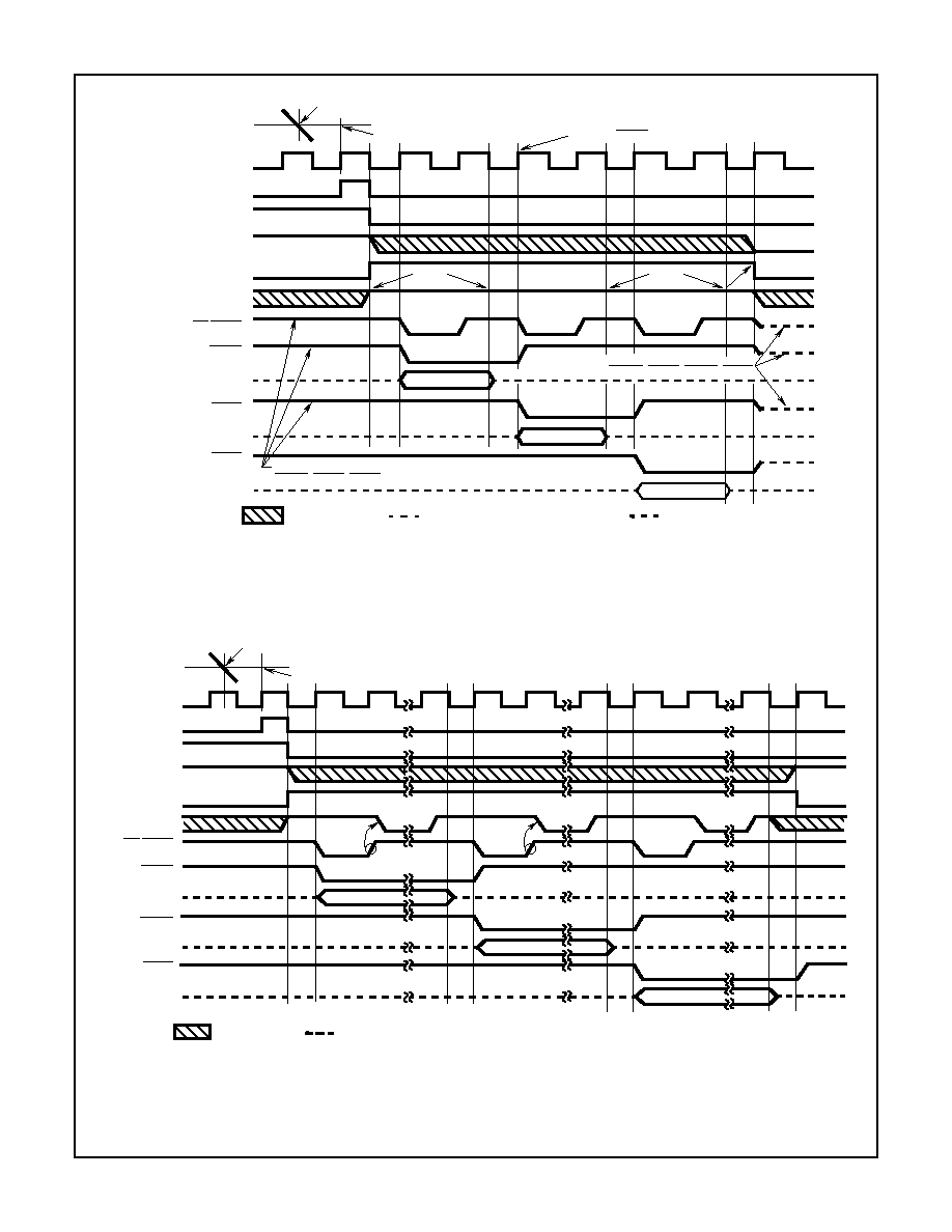
FIGURE 5. HANDSHAKE MODE TIMING DIAGRAM
CLOCK 1 H
L
(PIN 25)
EITHER:
MODE PIN
OR
INTERNAL
LATCH PULSE IF
MODE "HI"
H
L
H
L
UART
NORM
DON'T CARE
DON'T CARE
DON'T CARE
STABLE
DATA VALID, STABLE
DATA VALID, STABLE
EXT
EXT
t
MW
t
SM
t
CWH
H
L
H
L
H
L
H
L
INTERNAL
MODE
IGNORED
IGNORED
CE/LD
SEN
(EXTERNAL
SIGNAL)
HBEN
O/R, POL
01-14
LBEN
BITS 1-5
t
ME
t
MB
t
CEL
t
CEH
t
SS
t
CBL
t
CDH
t
CDL
t
CBH
t
CBZ
t
CEZ
THREE-STATE WITH PULLUP
THREE-STATE
-16 HAS EXTRA (MBEN) PHASE
HANDSHAKE MODE
OR
TRIGGERED BY
ICL8052/ICL7104, ICL8068/ICL7104

5-17
FIGURE 6A. PHASE I AUTO-ZERO
FIGURE 6B. PHASE II INTEGRATE INPUT
FIGURE 6C. PHASE III + DEINTEGRATE
FIGURE 6D. PHASE III DEINTEGRATE
A2
+
-
A3
+
-
INTEGRATOR
COMP.
A1
+
-
BUFFER
C
INT
1
R
INT
C
AZ
ZERO
CROSS.
DET.
POL
CL
2
3
6
7
8
9
AN
I/P
CL
ZERO
CROSSING
F/F
Q
D
V
REF
C
REF
-
+
4
A2
+
-
A3
+
-
INTEGRATOR
COMP.
A1
+
-
BUFFER
C
INT
1
R
INT
C
AZ
ZERO
CROSS.
DET.
POL
CL
2
3
6
7
8
9
AN
I/P
CL
ZERO
CROSSING
F/F
Q
D
CL
POL
F/F
Q
D
PHASE II
POL
V
REF
C
REF
-
+
4
A2
+
-
A3
+
-
INTEGRATOR
COMP.
A1
+
-
BUFFER
C
INT
1
R
INT
C
AZ
ZERO
CROSS.
DET.
POL
CL
2
3
6
7
8
9
+AN
I/P
CL
ZERO
CROSSING
F/F
Q
D
V
REF
C
REF
-
+
4
A2
+
-
A3
+
-
INTEGRATOR
COMP.
A1
+
-
BUFFER
C
INT
1
R
INT
C
AZ
ZERO
CROSS.
DET.
POL
CL
2
3
6
7
8
9
-AN
I/P
CL
ZERO
CROSSING
F/F
Q
D
V
REF
C
REF
-
+
4
ICL8052/ICL7104, ICL8068/ICL7104
5-18
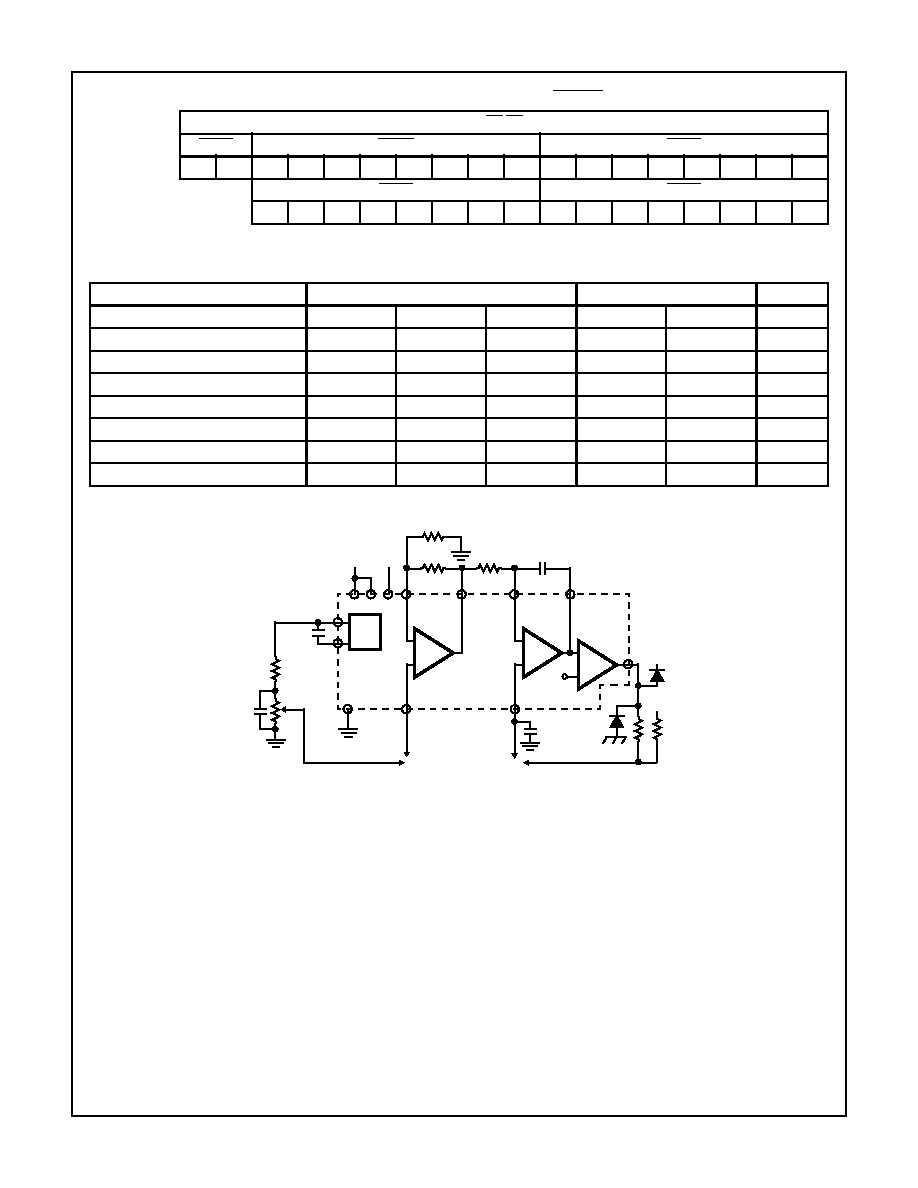
Buffer Gain
At the end of the auto-zero interval, the instantaneous noise
voltage on the auto-zero capacitor is stored, and subtracts
from the input voltage while adding to the reference voltage
during the next cycle. The result is that this noise voltage
effectively is somewhat greater than the input noise voltage
of the buffer itself during integration. By introducing some
voltage gain into the buffer, the effect of the auto-zero noise
(referred to the input) can be reduced to the level of the
inherent buffer noise. This generally occurs with a buffer gain
of between 3 and 10. Further increase in buffer gain merely
increases the total offset to be handled by the auto-zero
loop, and reduces the available buffer and integrator swings,
without improving the noise performance of the system. The
circuit recommended for doing this with the
ICL8068/ICL7104 is shown in Figure 7. With careful layout,
the circuit shown can achieve effective input noise voltages
on the order of 1 to 2
µ
V, allowing full 16-bit use with full scale
inputs of a low as 150mV. Note that at this level, thermoelec-
tric EMFs between PC boards, IC pins, etc., due to local
temperature changes can be very troublesome. For further
discussion, see Application Note AN030.
ICL8052 vs ICL8068
The ICL8052 offers significantly lower input leakage currents
than the ICL8068, and may be found preferable in systems
with high input impedances. However, the ICL8068 has
substantially lower noise voltage, and for systems where
system noise is a limiting factor, particularly in low signal
level conditions, will give better performance.
TABLE 3. THREE-STATE BYTE FORMATS AND ENABLE PINS
CE/LD
HBEN
MBEN
LBEN
ICL7104-16
POL
O/R
B16
B15
B14
B13
B12
B11
B10
B9
B8
B7
B6
B5
B4
B3
B2
B1
HBEN
LBEN
ICL7104-14
POL
O/R
B14
B13
B12
B11
B10
B9
B8
B7
B6
B5
B4
B3
B2
B1
TABLE 4. TYPICAL COMPONENT VALUES (V++ = +15V, V+ = 5V, V- = 5V, V- = -15V, f
CLOCK
= 200kHz)
ICL8052/8068 WITH
ICL7104-16
ICL7104-14
UNIT
Full scale V
IN
200
800
4000
100
4000
mV
Buffer Gain
10
1
1
10
1
V/V
R
INT
100
43
200
47
180
k
C
INT
0.33
0.33
0.33
0.1
0.1
µ
F
C
AZ
1
1
1
1
1
µ
F
C
REF
10
1
1
10
1
µ
F
V
REF
100
400
2000
50
2000
mV
Resolution
3.1
12
61
6.1
244
µ
V
FIGURE 7. ADDING BUFFER GAIN TO ICL8068
A2
+
-
A3
+
-
INTEG.
COMP.
A1
+
-
BUFFER
14
11
9
INT OUT
-INT IN
BUF OUT
10
-
BUF IN
-1.2V
2
-15V
+5V
R
INT
C
INT
1
-15V
7
8
+15V
12
+INT IN
13
8068
INT.
REF.
6
3
+BUF IN
5
REF
OUT
5k
10k
300pF
COMP
OUT
100k
10-50K
TO ICL7104
ICL8052/ICL7104, ICL8068/ICL7104
5-19
Component Value Selection
For optimum performance of the analog section, care must
be taken in the selection of values for the integrator capacitor
and resistor, auto-zero capacitor, reference voltage, and
conversion rate. These values must be chosen to suit the
particular application.
Integrating Resistor
The integrating resistor is determined by the full scale input
voltage and the output current of the buffer used to charge
the integrator capacitor. This current should be small
compared to the output short circuit current such that
thermal effects are kept to a minimum and linearity is not
affected. Values of 5 to 40
µ
A give good results with a
nominal of 20
µ
A. The exact value may be chosen by:
NOTE: If gain is used in the buffer amplifier then
Integrating Capacitor
The product of integrating resistor and capacitor is selected
to give 9 volt swing for full scale inputs. This is a compromise
between possibly saturating the integrator (at +14 volts) due
to tolerance build-up between the resistor, capacitor and
clock and the errors a lower voltage swing could induce due
to offsets referred to the output of the comparator. In
general, the value of C
INT
is given by:
A very important characteristic of the integrating capacitor is
that it have low dielectric absorption to prevent roll-over or
ratiometric errors. A good test for dielectric absorption is to
use the capacitor with the input tied to the reference.
This ratiometric condition should read half scale (100...000)
and any deviation is probably due to dielectric absorption.
Polypropylene capacitors give undetectable errors at reason-
able cost. Polystyrene and polycarbonate capacitors may
also be used in less critical applications.
Auto-Zero and Reference Capacitor
The size of the auto-zero capacitor has some influence on
the noise of the system, a large capacitor giving less noise.
The reference capacitor should be large enough such that
stray capacitance to ground from its nodes is negligible.
NOTE: When gain is used in the buffer amplifier the reference
capacitor should be substantially larger than the auto-zero capacitor.
As a rule of thumb, the reference capacitor should be approximately
the gain times the value of the auto-zero capacitor. The dielectric
absorption of the reference cap and auto-zero cap are only important
at power-on or when the circuit is recovering from an overload. Thus,
smaller or cheaper caps can be used here if accurate readings are
not required for the first few seconds of recovery.
Reference Voltage
The analog input required to generate a full scale output is
V
IN
= 2V
REF
.
The stability of the reference voltage is a major factor in the
overall absolute accuracy of the converter. The resolution of
the ICL7104 at 16 bits is one part in 65536, or 15.26ppm.
Thus, if the reference has a temperature coefficient of
50ppm/C (on board reference) a temperature change of
1/3C will introduce a one-bit absolute error. For this reason,
it is recommended that an external high quality reference be
used where the ambient temperature is not controlled or
where high-accuracy absolute measurements are being
made.
R
INT
full scale voltage (see note)
20
µ
A
-------------------------------------------------------------------------
=
R
INT
Buffe rGain
(
)
(full scale voltage)
20
µ
A
----------------------------------------------------------------------------------------
=
C
INT
(32768 for - 16)
(8192 for -14)
20
µ
A
◊
clock period
◊
Integrator Output Voltage Swing
----------------------------------------------------------------------------------------------------------
=
COUNTS
PHASE I
PHASE II
PHASE III
-16
32768
32768
65536
-14
8192
8192
16384
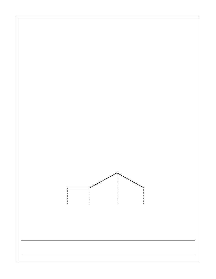
FIGURE 8. CONVERSION TIMING
POLARITY
DETECTED
ZERO CROSSING
OCCURS
ZERO CROSSING
DETECTED
DEINT PHASE III
INT PHASE II
AZ PHASE I
AZ
INTEGRATOR
OUTPUT
INTERNAL CLOCK
INTERNAL LATCH
STATUS OUTPUT
NUMBER OF COUNTS TO ZERO CROSSING
PROPORTIONAL TO V
IN
AFTER ZERO CROSSING,
ANALOG SECTION WILL
BE IN AUTOZERO
CONFIGURATION
ICL8052/ICL7104, ICL8068/ICL7104

5-20
Detailed Description
DIGITAL SECTION
The digital section includes the clock oscillator circuit, a
16-bit or 14-bit binary counter with output latches and TTL-
compatible three-state output drivers, polarity, over-range
and control logic and UART handshake logic, as shown in
the Block Diagram Figure 9 (16-bit version shown).
Throughout this description, logic levels will be referred to as
"low" or "high". The actual logic levels are defined under
"ICL7104 Electrical Specification". For minimum power con-
sumption, all inputs should swing from GND (low) to V+
(high). Inputs driven from TTL gates should have 3 - 5k
pullup resistors added for maximum noise immunity.
MODE Input
The MODE input is used to control the output mode of the
converter. When the MODE pin is connected to GND or left
open (this input is provided with a pulldown resistor to
ensure a low level when the pin is left open), the converter is
in its "Direct" output mode, where the output data is directly
accessible under the control of the chip and byte enable
inputs. When the MODE input is pulsed high, the converter
enters the UART handshake mode and outputs the data in
three bytes for the 7104-16 or two bytes for the 7104-14 then
returns to "direct" mode. When the MODE input is left high,
the converter will output data in the handshake mode at the
end of every conversion cycle. (See section entitled "Hand-
shake Mode" for further details).
STATUS Output
During a conversion cycle, the STATUS output goes high at
the beginning of Input Integrate (Phase II), and goes low
one-half clock period after new data from the conversion has
been stored in the output latches. See Figure 8 for details of
this timing. This signal may be used as a "data valid" flag
(data never changes while STATUS is low) to drive inter-
rupts, or for monitoring the status of the converter.
TABLE 5. THREE-STATE BYTE FORMATS AND ENABLE PINS
CE/LD
HBEN
MBEN
LBEN
ICL7104-16
POL
O/R
B16
B15
B14
B13
B12
B11
B10
B9
B8
B7
B6
B5
B4
B3
B2
B1
HBEN
LBEN
ICL7104-14
POL
O/R
B14
B13
B12
B11
B10
B9
B8
B7
B6
B5
B4
B3
B2
B1
FIGURE 9. DIGITAL SECTION
HBEN
MBEN
LBEN
CE/LD
OSCILLATOR
27
SEND
21
MODE
25
CLOCK
23
CLOCK
24
2
STATUS
26
R/H
(2)
(3)
AND CLOCK
CIRCUITRY
18/16 THREE-STATE OUTPUTS
18/16 LATCHES
18/16 BIT COUNTER
LATCH
CLOCK
HANDSHAKE
LOGIC
(-16 ONLY)
CONVERSION
CONTROL
LOGIC
INITIAL
CLEAR
CLOCK
(1)
COMP OUT
AZ
INT
DEINT(+)
DEINT(-)
TO
ANALOG
SECTION
ICL8052/ICL7104, ICL8068/ICL7104

5-21
Run/Hold Input
When the Run/Hold input is connected to V+ or left open
(this input has pullup resistor to ensure a high level when the
pin is left open), the circuit will continuously perform
conversion cycles, updating the output latches at the end of
every Deintegrate (Phase III) portion of the conversion cycle
(See Figure 8). (See under "Handshake Mode" for
exception.) In this mode of operation, the conversion cycle
will be performed in 131,072 for 7104-16 and 32768 for
7104-14 clock periods, regardless of the resulting value.
If Run/Hold goes low at any time during Deintegrate (Phase
III) after the zero crossing has occurred, the circuit will
immediately terminate Deintegrate and jump to Auto-Zero.
This feature can be used to eliminate the time spent in
Deintegrate after the zero-crossing. If Run/Hold stays or
goes low, the converter will ensure a minimum Auto-Zero
time, and then wait in Auto-Zero until the Run/Hold input
goes high. The converter will begin the Integrate (Phase II)
portion of the next conversion (and the STATUS output will
go high) seven clock periods after the high level is detected
at Run/Hold. See Figure 10 for details.
Using the Run/Hold input in this manner allows an easy
"convert on demand" interface to be used. The converter
may be held at idle in Auto-Zero with Run/Hold low. When
Run/Hold goes high the conversion is started, and when the
STATUS output goes low the new data is valid (or trans-
ferred) to the UART - see Handshake Mode). Run/Hold may
now go low terminating Deintegrate and ensuring a minimum
Auto-Zero time before stopping to wait for the next
conversion. Alternately, Run/Hold can be used to minimize
conversion time by ensuring that it goes low during Deinte-
grate, after zero crossing, and goes high after the hold point
is reached. The required activity on the Run/Hold input can
be provided by connecting it to the CLOCK3 (-14), CLOCK2
(-16) Output. In this mode the conversion time is dependent
on the input value measured. Also refer to Intersil Application
Bulletin A030 for a discussion of the effects this will have on
Auto-Zero performance.
If the Run/Hold input goes low and stays low during Auto-
Zero (Phase I), the converter will simply stop at the end of
the Auto-Zero and wait for Run/Hold to go high. As above,
Integrate (Phase II) begins seven clock periods after the high
level is detected.
Direct Mode
When the MODE pin is left at a low level, the data outputs
[bits 1 through 8 low order byte, See Table 3 for format of
middle (-16) and high order bytes] are accessible under
control of the byte and CHIP ENABLE terminals as inputs.
These ENABLE inputs are all active low, and are provided
with pullup resistors to ensure an inactive high level when
left open. When the CHIP ENABLE input is low, taking a byte
ENABLE input low will allow the outputs of that byte to
become active (three-stated on). This allows a variety of
parallel data accessing techniques to be used. The timing
requirements for these outputs are shown under AC
Specifications and Table 1.
It should be noted that these control inputs are asynchro-
nous with respect to the converter clock - the data may be
accessed at any time. Thus it is possible to access the data
while it is being updated, which could lead to scrambled
data. Synchronizing the access of data with the conversion
cycle by monitoring the STATUS output will prevent this.
Data is never updated while STATUS is low. Also note the
potential bus conflict described under "Initial Clear Circuitry".
Handshake Mode
The handshake output mode is provided as an alternative
means of interfacing the ICL7104 to digital systems, where
the A/D converter becomes active in controlling the flow of
data instead of passively responding to chip and byte
ENABLE inputs. This mode is specifically designed to allow
a direct interface between the ICL7104 and industry-stan-
dard UARTs (such as the Intersil CMOS UARTs, IM6402/3)
with no external logic required. When triggered into the
handshake mode, the ICL7104 provides all the control and
flag signals necessary to sequence the three (ICL7106-16)
or two (ICL7104-14) bytes of data into the UART and initiate
their transmission in serial form. This greatly eases the task
and reduces the cost of designing remote data acquisition
stations using serial data transmission to minimize the
number of lines to the central controlling processor.
FIGURE 10. RUN/HOLD OPERATION
DEINT TERMINATED
AT ZERO CROSSING
STATIC IN
HOLD STATE
INT
PHASE
7 COUNTS
INTEGRATOR
OUTPUT
INTERNAL
CLOCK
INTERNAL
LATCH
STATUS
OUTPUT
RUN/HOLD
INPUT
DETECTION
-14
7161
8185
-16
28665
32761
OPTION
MIN
MAX
ICL8052/ICL7104, ICL8068/ICL7104
5-22
Entry into the handshake mode will occur if either of two
conditions are fulfilled; first, if new data is latched (i.e., a
conversion is completed) while MODE pin (pin 27) is high, in
which case entry occurs at the end of the latch cycle; or
secondly, if the MODE pin goes from low to high, when entry
will occur immediately (if new data is being latched, entry is
delayed to the end of the latch cycle). While in the
handshake mode, data latching is inhibited, and the MODE
pin is ignored. (Note that conversion cycles will continue in
the normal manner). This allows versatile initiation of hand-
shake operation without danger of false data generation; if
the MODE pin is held high, every conversion (other than
those completed during handshake operations) will start a
new handshake operation, while if the MODE pin is pulsed
high, handshake operations can be obtained "on demand."
When the converter enters the handshake mode, or when
the MODE input is high, the chip and byte ENABLE termi-
nals become TTL-compatible outputs which provide the con-
trol signals for the output cycle. The Send ENABLE pin
(SEN) (pin 29) is used as an indication of the ability of the
external device to receive data. The condition of the line is
sensed once every clock pulse, and if it is high, the next (or
first) byte is enabled on the next rising CLOCK 1 (pin 25)
clock edge, the corresponding byte ENABLE line goes low,
and the CHIP ENABLE / LOAD pin (pin 30) (CE/LD) goes
low for one full clock pulse only, returning high.
On the next falling CLOCK 1 clock pulse edge, if SEN
remains high, or after it goes high again, the byte output
lines will be put in the high impedance state (or three-stated
off). One half pulse later, the byte ENABLE pin will be
cleared high, and (unless finished) the CE/LD and the next
byte ENABLE pin will go low. This will continue until all three
(2 in the case of the 14-bit device) bytes have been sent.
The bytes are individually put into the low impedance state
i.e.: three-stated on during most of the time that their byte
ENABLE pin is (active) low. When receipt of the last byte has
been acknowledged by a high SEN, the handshake mode
will be cleared, re-enabling data latching from conversion,
and recognizing the condition of the MODE pin again. The
byte and CHIP ENABLE will be three-stated off, if MODE is
low, but held by their (weak) pullups. These timing relation-
ships are illustrated in Figures 11, 12, and 13, and Table 2.
Figure 11 shows the sequence of the output cycle with SEN
held high. The handshake mode (Internal MODE high) is
entered after the data latch pulse (since MODE remains high
the CE/LD, LBEN, MBEN and HBEN terminals are active as
outputs). The high level at the SEN input is sensed on the
same high to low internal clock edge. On the next to high
internal clock edge, the CE/LD and the HBEN outputs
assume a low level and the high-order byte (POL and OR,
and except for -16, Bits 9 - 14) outputs are enabled. The
CE/LD output remains low for one full internal clock period
only, the data outputs remain active for 1
1
/
2
internal clock
periods, and the high byte ENABLE remains low for two
clock periods. Thus the CE/LD output low level or low to high
edge may be used as a synchronizing signal to ensure valid
data, and the byte ENABLE as an output may be used as a
byte identification flag. With SEN remaining high the con-
verter completes the output cycle using CE/LD, MBEN and
LBEN while the remaining byte outputs (see Table 3) are
activated. The handshake mode is terminated when all bytes
are sent (3 for -16, 2 for -14).
Figure 12 shows an output sequence where the SEN input is
used to delay portions of the sequence, or handshake, to
ensure correct data transfer. This timing diagram shows the
relationships that occur using an industry-standard IM6402/3
CMOS UART to interface to serial data channels. In this
interface, the SEN input to the ICL7104 is driven by the
TBRE (Transmitter Buffer Register Empty) output of the
UART, and the CE/LD terminal of the ICL7104 drives the
TBRL (Transmitter Buffer Register Load) input to the UART.
The data outputs are paralleled into the eight Transmitter
Buffer Register inputs.
Assuming the UART Transmitter Buffer Register is empty,
the SEN input will be high when the handshake mode is
entered after new data is stored. The CE/LD and HBEN ter-
minals will go low after SEN is sensed, and the high order
byte outputs become active. When CE/LD goes high at the
end of one clock period, the high order byte data is clocked
into the UART Transmitter Buffer Register. The UART TBRE
output will now go low, which halts the output cycle with the
HBEN output low, and the high order byte outputs active.
When the UART has transferred the data to the Transmitter
Register and cleared the Transmitter Buffer Register, the
TBRE returns high. On the next ICL7104 internal clock high
to low edge, the high order byte outputs are disabled, and
one-half internal clock later, the HBEN output returns high.
At the same time, the CE/LD and MBEN (-16) or LBEN out-
puts go low, and the corresponding byte outputs become
active. Similarly, when the CE/LD returns high at the end of
one clock period, the enabled data is clocked into the UART
Transmitter Buffer Register, and TBRE again goes low.
When TBRE returns to a high it will be sensed on the next
ICL7104 internal clock high to low edge, disabling the data
outputs. For the 16-bit device, the sequence is repeated for
LBEN. One-half internal clock later, the handshake mode will
be cleared, and the chip and byte ENABLE terminals return
high and stay active (as long as MODE stays high).
With the MODE input remaining high as in these examples,
the converter will output the results of every conversion
except those completed during a handshake operation. By
triggering the converter into handshake mode with a low to
high edge on the MODE input, handshake output sequences
may be performed on demand. Figure 13 shows a
handshake output sequence triggered by such an edge. In
addition, the SEN input is shown as being low when the con-
verter enters handshake mode. In this case, the whole out-
put sequence is controlled by the SEN input, and the
sequence for the first (high order) byte is similar to the
sequence for the other bytes. This diagram also shows the
output sequence taking longer than a conversion cycle. Note
that the converter still makes conversions, with the STATUS
output and Run/Hold input functioning normally. The only
difference is that new data will not be latched when in
handshake mode, and is therefore lost.
ICL8052/ICL7104, ICL8068/ICL7104
5-23
FIGURE 11. HANDSHAKE WITH SEN HELD POSITIVE
DATA VALID
DATA VALID
DATA VALID
THREE-STATE WITH PULLUP
THREE-STATE HIGH IMPEDANCE
DON'T CARE
INTEGRATOR OUTPUT
INTERNAL CLOCK
INTERNAL LATCH
STATUS OUTPUT
MODE INPUT
INTERNAL MODE
SEN INPUT
CE/LOAD
UART
HIGH BYTE DATA
LOW BYTE DATA
LOW BYTE DATA
NORM
MODE HIGH ACTIVATES
CE/LD, HBEN, LBEN
HBEN
LBEN
LBEN
SENSED
SEN
ZERO-CROSSING DETECTED
ZERO-CROSSING OCCURS
MODE LOW NOT IN HANDSHAKE MODE
DISABLES OUTPUTS CE/LD, HBEN, MBEN, LBEN
SENSED
SEN
TERMINATES
UART MODE
FOR -16 MBEN SEQUENCE INSERTED HERE
FIGURE 12. HANDSHAKE - TYPICAL UART INTERFACE TIMING
DATA VALID
THREE-STATE HIGH IMPEDANCE
DON'T CARE
INTEGRATOR
INTERNAL
INTERNAL
STATUS
MODE
INTERNAL
SEN INPUT
CE/LOAD
UART
HIGH BYTE
MIDDLE
LOW BYTE
NORM
HBEN
MBEN
LBEN
ZERO-CROSSING DETECTED
ZERO-CROSSING OCCURS
OUTPUT
CLOCK
LATCH
OUTPUT
INPUT
MODE
DATA
BYTE DATA
DATA
DATA VALID
DATA VALID
(UART TBRE)
(UART TBRL)
ICL8052/ICL7104, ICL8068/ICL7104
5-24
Initial Clear Circuitry
The internal logic of the 7104 is supplied by an internal
regulator between V++ and Digital Ground. The regulator
includes a low-voltage detector that will clear various
registers. This is intended to ensure that on initial power-up,
the control logic comes up in Auto-Zero, with the 2nd, 3rd,
and 4th MSB bits cleared, and the "mode" F/F cleared (i.e.,
in "direct" mode). This, however, will also clear these regis-
ters if the supply voltage "glitches" to a low enough value.
Additionally, if the supply voltage comes up too fast, this
clear pulse may be too narrow for reliable clearing. In gen-
eral, this is not a problem, but if the UART internal "MODE"
F/F should come up set, the byte and chip ENABLE lines will
become active outputs. In many systems this could lead to
bus conflicts, especially in non-handshake systems. In any
case, SEN should be high (held high for non-handshake sys-
tems) to ensure that the MODE F/F will be cleared as fast as
possible (see Figure 11 for timing). For these and other
reasons, adequate supply bypass is recommended.
Oscillator
The ICL7104-14 is provided with a versatile three terminal
oscillator to generate the internal clock. The oscillator may
be overdriven, or may be operated as an RC or crystal
oscillator.
Figure 14 shows the oscillator configured for RC operation.
The internal clock will be of the same frequency and phase
as the voltage on the CLOCK 3 pin. The resistor and
capacitor should be connected as shown. The circuit will
oscillate at a frequency given by f = 0.45/RC. A 50 - 100k
resistor is recommended for useful ranges of frequency. For
optimum 60Hz line rejection, the capacitor value should be
chosen such that 32768 (-16), 8192 (-14) clock periods is
close to an integral multiple of the 60Hz period.
As a result of pin count limitations, the ICL7104-16 has only
CLOCK 1 and CLOCK 2 available, and cannot be used as
an RC oscillator. The internal clock will correspond to the
inverse of the signal on CLOCK 2. Figure 15 shows a crystal
oscillator circuit, which can be used with both 7104 versions.
If an external clock is to be used, it should be applied to
CLOCK 1. This internal clock will correspond to the signal
applied to this pin.
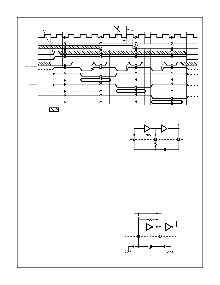
FIGURE 13. HANDSHAKE TRIGGERED BY MODE
DATA VALID
INTERNAL
INTERNAL
STATUS
MODE
INTERNAL
SEN INPUT
CE/LOAD
UART
HIGH BYTE
MIDDLE
LOW BYTE
NORM
HBEN
MBEN
LBEN
ZERO-CROSSING DETECTED
ZERO-CROSSING OCCURS
CLOCK
LATCH
OUTPUT
INPUT
MODE
DATA
BYTE DATA
DATA
DATA VALID
DATA VALID
STATUS OUTPUT UNAFFECTED
BY UART MODE
LATCH PULSE INHIBITED
IN UART MODE
THREE-STATE WITH PULLUP
THREE-STATE HIGH IMPEDANCE
DON'T CARE
POSITIVE TRANSITION
CAUSES ENTRY INTO
UART MODE
DEINT PHASE III
AS OUTPUT
NOTE: Clock 3 has the same output drive as the bit outputs.
FIGURE 14. RC OSCILLATOR (ICL7104-14 ONLY)
CLOCK
25
26
R
C
2
CLOCK
3
CLOCK
1
24
f
OSC
= 0.45/RC
FIGURE 15. CRYSTAL OSCILLATOR
CLOCK
25
26
2
CLOCK
1
V+
CAPACITOR VALUE
DEPENDS ON CRYSTAL
TYP 0-30pF
CRYSTAL
ICL8052/ICL7104, ICL8068/ICL7104
5-25
Power Supply Sequencing
Because of the nature of the CMOS process used to
fabricate the ICL7104, and the multiple power supplies
used, there are certain conditions of these supplies under
which a disabling and potentially damaging SCR action can
occur. All of these conditions involve the V+ supply (Norm
+5V) being more positive than the V++ supply. If there is
any possibility of this occurring during start-up, shut down,
under transient conditions during operation, or when insert-
ing a PC board into a "hot" socket, etc., a diode should be
placed between V+ and V++ to prevent it. A germanium or
Schottky rectifier diode would be best, but in most cases a
silicon rectifier is adequate.
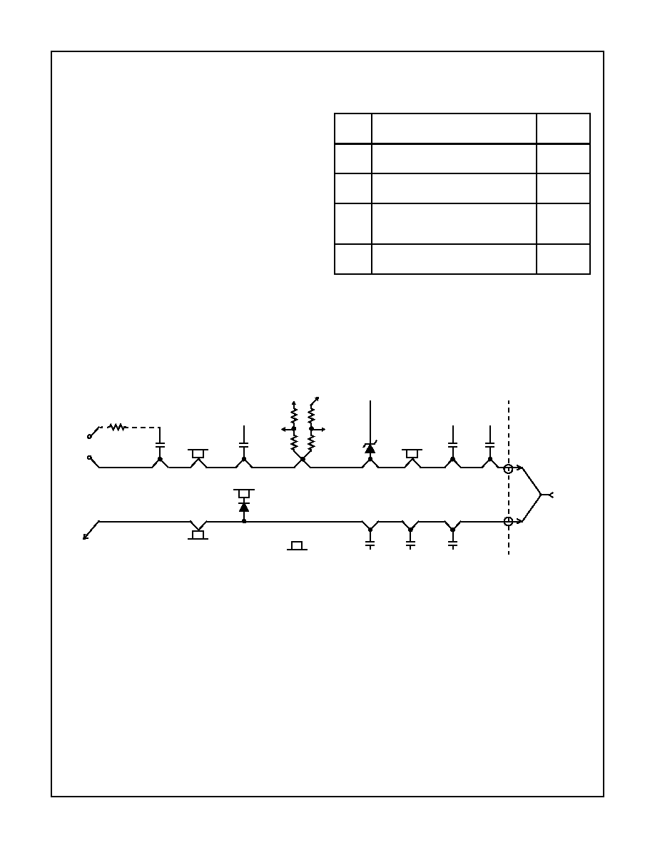
Analog and Digital Grounds
Extreme care must be taken to avoid ground loops in the
layout of ICL8068 or ICL8052/7104 circuits, especially in
16-bit and high sensitivity circuits. It is most important that
return currents from digital loads are not fed into the analog
ground line. A recommended connection sequence for the
ground lines is shown in Figure 16.
Application Notes
Some application notes that may be found useful are listed
here:
NOTE #
DESCRIPTION
AnswerFAX
DOC. #
AN016
"Selecting A/D Converters", by Dave
Fullagar
9016
AN017
"The Integrating A/D Converter", by Lee
Evans
9017
AN018
"Do's and Don'ts of Applying A/D
Converters," by Peter Bradshaw and Skip
Osgood
9018
AN030
"Building a Battery-Operated Auto
Ranging DVM with the ICL7106"
9030
FIGURE 16. GROUNDING SEQUENCE
DEVICE PIN
DIG GND
ICL7104
PIN 2
DIGITAL
LOGIC
V
IN
I/P
+
-
FILTER
CAP
8068 PIN 2
COMP
PIN 35
ICL7104
AN GND
C
AZ
V
REF
BUFF
-IN
(IF USED)
REF
VOLTAGE
BUFF
OUT
EXTERNAL
REFERENCE
(IF USED)
PIN 35
ICL7104
AN GND
+15V
-15V
+5V SUPPLY BYPASS CAPACITOR(S)
SUPPLY
RETURN
BOARD
EDGE
ICL8052/ICL7104, ICL8068/ICL7104
5-26
ICL7104 with ICL8052/8068 Integrating A/D Converter Equations
∑ Oscillator
CRYSTAL or RC (RC on -14 Part Only)
f
OSC
(Typ) 200kHz
f
OSC
= 0.45/RC (ICL7104-14 Only)
C
OSC
> 50pF and R
OSC
> 50K
∑ Oscillator Period
t
OSC
= 1/f
OSC
∑ Integration Clock Frequency
f
CLOCK
= f
OSC
∑ Integration Period
t
INT
= 8192 x t
OSC
(7104-14)
t
INT
= 32768 x t
OSC
(7104-16)
∑ 60/50Hz Rejection Criterion
t
INT
/t
60Hz
or t
INT
/t
50Hz
= Integer
∑ Optimum Integration Current
I
INT
= 20
µ
A
∑ Full Scale Analog Input Voltage
V
INFS
(Typ) = 200mV to 2V = 2V
REF
∑ Integrate Resistor
∑ Integrate Capacitor
∑ Integrator Output Voltage
V
INT
(Typ) = 9V
∑ Output Count
∑ Output Type:
Binary Amplitude with Polarity and Overrange Bits.
∑ Power Supply:
±
15V, +5V
V++ = +15V
V- = -15V
V+ = +5V
V
REF
1.75V
If V
REF
not used, float output pin.
∑ Auto Zero Capacitor Values
0.01
µ
F < C
AZ
< 1
µ
F
∑ Reference Capacitor Value
C
REF
= (Buffer Gain) x C
AZ
R
INT
Buffe rGain
(
)
V
INFS
◊
I
INT
-------------------------------------------------------------
=
C
INT
t
INT
(
)
I
INT
(
)
V
INT
--------------------------------
=
V
INT
t
INT
(
)
I
INT
(
)
C
INT
--------------------------------
=
Count
8192
V
IN
V
REF
---------------
◊
(7104-14)
=
Count
32768
V
IN
V
REF
---------------
◊
(7104-16)
=
FIGURE 17.
AUTOZERO
(COUNT)
24,576 - 8,193
98,304 - 32,769
INTEGRATE
(FIXED COUNT)
8192
32768
DEINTEGRATE
(COUNT)
0 - 16383
0 - 65535
ICL7104 - 14
ICL7104 - 16
CONVERSION TIME (IN CONTINUOUS MODE):
32,768
t
OSC
(7104 - 14)
131,072
t
OSC
(7104 - 16)
ICL8052/ICL7104, ICL8068/ICL7104
All Intersil semiconductor products are manufactured, assembled and tested under ISO9000 quality systems certification.
Intersil products are sold by description only. Intersil Corporation reserves the right to make changes in circuit design and/or specifications at any time without
notice. Accordingly, the reader is cautioned to verify that data sheets are current before placing orders. Information furnished by Intersil is believed to be accurate
and reliable. However, no responsibility is assumed by Intersil or its subsidiaries for its use; nor for any infringements of patents or other rights of third parties which
may result from its use. No license is granted by implication or otherwise under any patent or patent rights of Intersil or its subsidiaries.
For information regarding Intersil Corporation and its products, see web site http://www.intersil.com