 | –≠–ª–µ–∫—Ç—Ä–æ–Ω–Ω—ã–π –∫–æ–º–ø–æ–Ω–µ–Ω—Ç: ICL8069DC | –°–∫–∞—á–∞—Ç—å:  PDF PDF  ZIP ZIP |
1
Æ
CAUTION: These devices are sensitive to electrostatic discharge; follow proper IC Handling Procedures.
1-888-INTERSIL or 321-724-7143
|
Intersil (and design) is a registered trademark of Intersil Americas Inc.
Copyright © Intersil Americas Inc. 2003. All Rights Reserved
All other trademarks mentioned are the property of their respective owners.
Low Voltage Reference
The ICL8069 is a 1.2V temperature-compensated voltage
reference. It uses the band-gap principle to achieve excel-
lent stability and low noise at reverse currents down to 50
µ
A.
Applications include analog-to-digital converters, digital-to-
analog converters, threshold detectors, and voltage
regulators. Its low power consumption makes it especially
suitable for battery operated equipment.
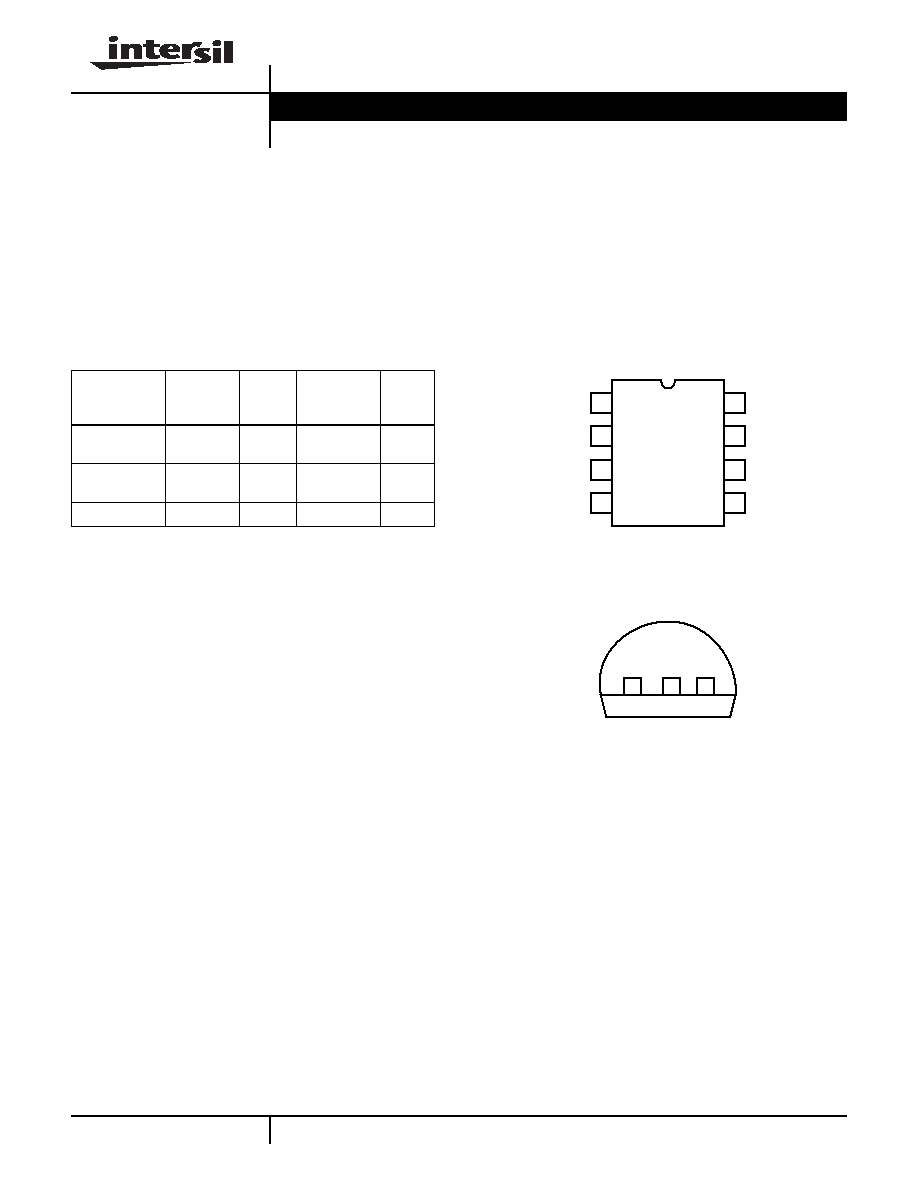
Ordering Information
Features
∑ Low Bias Current (Min) . . . . . . . . . . . . . . . . . . . . . . .50
µ
A
∑ Low Dynamic Impedance
∑ Low Reverse Voltage
∑ Low Cost
Pinouts
PART
NUMBER
MAXIMUM
TEMPCO
TEMP.
RANGE
(
o
C)
PACKAGE
PKG.
NO.
ICL8069CCZR
0.005%/
o
C
0 to 70
SIP Package
(TO-92)
Z3.05
ICL8069DCZR
0.01%/
o
C
0 to 70
SIP Package
(TO-92)
Z3.05
ICL8069CCBA
0.005%/
o
C
0 to 70
8 Ld SOlC
M8.15
NC
NC
NC
V-
1
2
3
4
8
7
6
5
V+
NC
NC
NC
1
2
3
NC
V+
V-
ICL8069 (SOIC)
TOP VIEW
ICL8069 (SIP TO-92)
TOP VIEW
FN3172.2
ICL8069
Data Sheet
May 2003
2
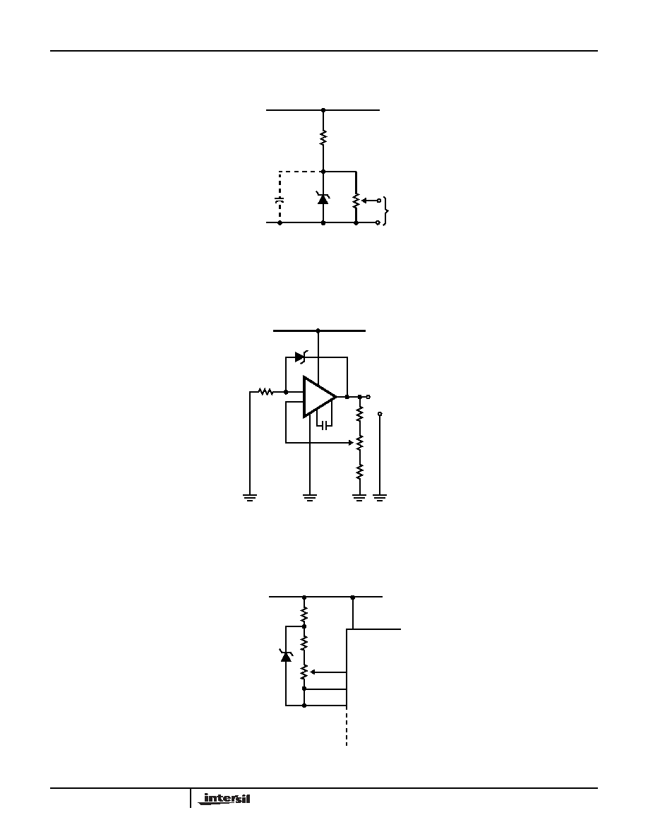
Functional Block Diagrams
SIMPLE REFERENCE (1.2V OR LESS)
BUFFERED 10V REFERENCE USING A SINGLE SUPPLY
DOUBLE REGULATED 100mV REFERENCE FOR ICL7107 ONE-CHIP DPM CIRCUIT
+5V
6.8k
10k
ICL8069
4.7
µ
F
2
V
OUT
1
(NOTE 1)
+10V
OUT
LM108
ICL8069
1
2
3
7
6
8
4
5
2
1k
1k
8.2k
-
+
15k
+15V
0.01
µ
F
2.2k
+V
+5V
REF HI
COMMON
REF LO
1
2
ICL8069
10k
1k
ICL7107
ICL8069
ICL8069
3
ICL8069
Absolute Maximum Ratings
Thermal Information
Reverse Voltage . . . . . . . . . . . . . . . . . . . . . . . . . . . . . . . See Note 3
Forward Current. . . . . . . . . . . . . . . . . . . . . . . . . . . . . . . . . . . . 10mA
Reverse Current. . . . . . . . . . . . . . . . . . . . . . . . . . . . . . . . . . . . 10mA
Operating Conditions
Temperature Ranges
ICL8069C . . . . . . . . . . . . . . . . . . . . . . . . . . . . . . . . . . 0
o
C to 70
o
C
Thermal Resistance (Typical, Note 1)
JA
(
o
C/W)
JC
(
o
C/W)
SOIC Package . . . . . . . . . . . . . . . . . . .
170
N/A
SIP (TO-92) Package. . . . . . . . . . . . . .
200
N/A
Power Dissipation Limited by MAX Forward/Reverse Current
Maximum Junction Temperature (SOIC Package) . . . . . . . . .150
o
C
Maximum Storage Temperature Range . . . . . . . . . -65
o
C to 150
o
C
Maximum Lead Temperature (Soldering 10s) . . . . . . . . . . . . .300
o
C
(SOIC - Lead Tips Only)
CAUTION: Stresses above those listed in "Absolute Maximum Ratings" may cause permanent damage to the device. This is a stress only rating and operation of the
device at these or any other conditions above those indicated in the operational sections of this specification is not implied.
NOTE:
1.
JA
is measured with the component mounted on an evaluation PC board in free air.
Electrical Specifications
T
A
= 25
o
C Unless Otherwise Specified
PARAMETER
TEST CONDITIONS
MIN
TYP
MAX
UNITS
Reverse Breakdown Voltage
I
R
= 500
µ
A
1.20
1.23
1.25
V
Reverse Breakdown Voltage Change
50
µ
A
l
R
5mA
-
15
20
mV
Reverse Dynamic Impedance
l
R
= 50
µ
A
-
1
2
l
R
= 50
0µ
A
-
1
2
Forward Voltage Drop
l
F
= 500
µ
A
-
0.7
1
V
RMS Noise Voltage
10Hz
F
10kHz, l
R
= 50
0µ
A
-
5
-
µ
V
Long Term Stability
l
R
= 4.75mA, T
A
= 25
o
C
-
1
-
ppm/kHR
Breakdown Voltage Temperature Coefficient
I
R
= 500
µ
A, T
A
= Operating
Temperature Range
ICL8069C
-
-
0.005
%/
o
C
ICL8069D
-
-
0.01
%/
o
C
Reverse Current Range
1.18V to 1.27V
0.050
-
5
mA
NOTES:
2. If circuit strays in excess of 200pF are anticipated, a 4.7
µ
F shunt capacitor will ensure stability under all operating conditions.
3. In normal use, the reverse voltage cannot exceed the reference voltage. However when plugging units into a powered-up test fixture, an
instantaneous voltage equal to the compliance of the test circuit will be seen. This should not exceed 20V.
4
ICL8069
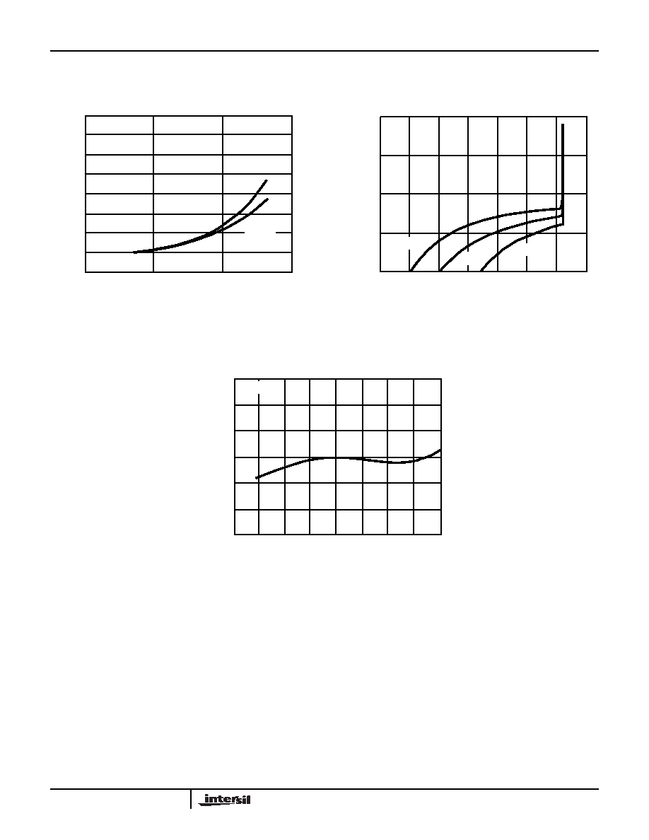
Typical Performance Curves
FIGURE 1. VOLTAGE CHANGE AS A FUNCTION OF
REVERSE CURRENT
FIGURE 2. REVERSE VOLTAGE AS A FUNCTION OF
CURRENT
FIGURE 3. REVERSE VOLTAGE AS A FUNCTION OF TEMPERATURE
14
12
10
-55
o
C
125
o
C
8
6
4
2
0
-2
REVERSE CURRENT (A)
10
µ
100
µ
1mA
10mA
OUT
P
UT
VOLT
AGE CH
ANGE (m
V
)
25
o
C,
100mA
-55
o
C
REVERSE VOLTAGE (V)
0.2
0.4
0.6
0.8
1.0
1.2
1.4
1mA
100
µ
10
µ
1
µ
R
E
VERS
E
CURRENT
(A)
25
o
C
125
o
C
I
R
= 500
µ
A
TEMPERATURE (
o
C)
25
50
75
100
125
0
-25
-50
1.245
1.240
1.235
1.230
1.225
1.220
1.215
OUTPUT VOLTA
GE
(V)

5
ICL8069
Single-In-Line Plastic Packages (SIP)
L
D
W
e
e
1
R
E
S1
A
(2X)
b
E-PIN ÿ 0.0625
NOTES:
1. Package body dimensions do not include any mold flash or pro-
trusions.
2. Package outline dimensions do not include burrs.
3. Controlling dimension: INCH.
Z3.05
(JEDEC STYLE TO-92 MODIFIED)
3 LEAD PLASTIC SINGLE-IN-LINE PACKAGE
SYMBOL
INCHES
MILLIMETERS
NOTES
MIN
MAX
MIN
MAX
A
0.170
0.195
4.32
4.95
1
b
0.014
0.020
0.36
0.51
2
E
0.130
0.155
3.30
3.94
1
e
0.045
0.055
1.14
1.40
-
e1
0.095
0.105
2.41
2.67
-
L
0.500
0.610
12.70
15.49
-
R
0.085
0.095
2.16
2.41
-
S1
0.045
0.060
1.14
1.52
-
W
0.016
0.022
0.41
0.56
2
D
0.175
0.195
4.45
4.95
1
4
o
6
o
4
o
6
o
-
Rev. 0 2/94

6
All Intersil U.S. products are manufactured, assembled and tested utilizing ISO9000 quality systems.
Intersil Corporation's quality certifications can be viewed at www.intersil.com/design/quality
Intersil products are sold by description only. Intersil Corporation reserves the right to make changes in circuit design, software and/or specifications at any time without
notice. Accordingly, the reader is cautioned to verify that data sheets are current before placing orders. Information furnished by Intersil is believed to be accurate and
reliable. However, no responsibility is assumed by Intersil or its subsidiaries for its use; nor for any infringements of patents or other rights of third parties which may result
from its use. No license is granted by implication or otherwise under any patent or patent rights of Intersil or its subsidiaries.
For information regarding Intersil Corporation and its products, see www.intersil.com
ICL8069
Small Outline Plastic Packages (SOIC)
INDEX
AREA
E
D
N
1
2
3
-B-
0.25(0.010)
C A
M
B S
e
-A-
L
B
M
-C-
A1
A
SEATING PLANE
0.10(0.004)
h x 45
o
C
H
µ
0.25(0.010)
B
M
M
NOTES:
1. Symbols are defined in the "MO Series Symbol List" in Section 2.2 of
Publication Number 95.
2. Dimensioning and tolerancing per ANSI Y14.5M-1982.
3. Dimension "D" does not include mold flash, protrusions or gate burrs.
Mold flash, protrusion and gate burrs shall not exceed 0.15mm (0.006
inch) per side.
4. Dimension "E" does not include interlead flash or protrusions. Inter-
lead flash and protrusions shall not exceed 0.25mm (0.010 inch) per
side.
5. The chamfer on the body is optional. If it is not present, a visual index
feature must be located within the crosshatched area.
6. "L" is the length of terminal for soldering to a substrate.
7. "N" is the number of terminal positions.
8. Terminal numbers are shown for reference only.
9. The lead width "B", as measured 0.36mm (0.014 inch) or greater
above the seating plane, shall not exceed a maximum value of
0.61mm (0.024 inch).
10. Controlling dimension: MILLIMETER. Converted inch dimensions
are not necessarily exact.
M8.15
(JEDEC MS-012-AA ISSUE C)
8 LEAD NARROW BODY SMALL OUTLINE PLASTIC
PACKAGE
SYMBOL
INCHES
MILLIMETERS
NOTES
MIN
MAX
MIN
MAX
A
0.0532
0.0688
1.35
1.75
-
A1
0.0040
0.0098
0.10
0.25
-
B
0.013
0.020
0.33
0.51
9
C
0.0075
0.0098
0.19
0.25
-
D
0.1890
0.1968
4.80
5.00
3
E
0.1497
0.1574
3.80
4.00
4
e
0.050 BSC
1.27 BSC
-
H
0.2284
0.2440
5.80
6.20
-
h
0.0099
0.0196
0.25
0.50
5
L
0.016
0.050
0.40
1.27
6
N
8
8
7
0
o
8
o
0
o
8
o
-
Rev. 0 12/93