 | –≠–ª–µ–∫—Ç—Ä–æ–Ω–Ω—ã–π –∫–æ–º–ø–æ–Ω–µ–Ω—Ç: ICM7211AI | –°–∫–∞—á–∞—Ç—å:  PDF PDF  ZIP ZIP |

1
August 2001
ICM7211A
4-Digit, LCD Display Driver
Features
∑ Four Digit Non-Multiplexed 7 Segment LCD Display
Outputs with Backplane Driver
∑ Complete Onboard RC Oscillator to Generate Backplane
Frequency
∑ Backplane Input/Output Allows Simple Synchronization
of Slave-Devices to a Master
∑ ICM7211A Devices Provide Separate Digit Select Inputs
to
Accept
Multiplexed
BCD
Input
(Pinout
and
Functionally Compatible with Siliconix DF411)
∑ ICM7211AM Devices Provide Data and Digit Address
Latches Controlled by Chip Select Inputs to Provide a
Direct High Speed Processor Interface
∑ Decodes Binary to Code B (0-9, Dash, E, H, L, P, Blank)
∑ Available in Surface Mount Package
Description
The ICM7211A (LCD) device constitutes a family of non-mul-
tiplexed four-digit seven-segment CMOS display decoder-
drivers.
The ICM7211A devices are configured to drive conventional
LCD displays by providing a complete RC oscillator, divider
chain, backplane driver, and 28 segment outputs.
This device is available with multiplexed or microprocessor
input configurations. The multiplexed versions provide four
data inputs and four Digit Select inputs. This configuration is
suitable for interfacing with multiplexed BCD or binary output
devices, such as the ICL7135. The microprocessor versions
provide data input latches and Digit Address latches under
control of high-speed Chip Select inputs. These devices sim-
plify the task of implementing a cost-effective alphanumeric
seven-segment display for microprocessor systems, without
requiring extensive ROM or CPU time for decoding and dis-
play updating.
The ICM7211A provides the "Code B" output code, i.e., 0-9,
dash, E, H, L, P, blank, but will correctly decode true BCD to
seven-segment decimal outputs.
Ordering Information
PART NUMBER
DISPLAY
TYPE
DISPLAY
DECODING
INPUT
INTERFACING
DISPLAY DRIVE
TYPE
TEMP.
RANGE (
o
C)
PACKAGE
PKG. NO.
ICM7211AlPL
LCD
Code B
Multiplexed
Direct Drive
-40◊ to 85◊
40 Ld PDIP
E40.6
ICM7211AMlPL
LCD
Code B
Microprocessor
Direct Drive
-40◊ to 85◊
40 Ld PDIP
E40.6
ICM7211AMlM44
LCD
Code B
Microprocessor
Direct Drive
-40◊ to 85◊
44 Ld MQFP
Q44.10x10
File Number
3158.4
CAUTION: These devices are sensitive to electrostatic discharge; follow proper IC Handling Procedures.
1-888-INTERSIL or 321-724-7143
|
Intersil and Design is a trademark of Intersil Americas Inc.
|
Copyright © Intersil Americas Inc. 2001

2
Pinouts
ICM7211A
(PDIP)
TOP VIEW
ICM7211AM
(PDIP)
TOP VIEW
ICM7211AM
(MQFP)
TOP VIEW
13
1
2
3
4
5
6
7
8
9
10
11
12
14
15
16
17
18
19
20
V
DD
e
1
g
1
f
1
BP
a
2
b
2
c
2
d
2
e
2
g
2
f
2
a
3
b
3
c
3
d
3
e
3
g
3
f
3
a
4
28
40
39
38
37
36
35
34
33
32
31
30
29
27
26
25
24
23
22
21
d
1
c
1
b
1
a
1
OSC
V
SS
D4
D3
D2
D1
f
4
g
4
e
4
d
4
c
4
b
4
DIGIT
SELECT
INPUTS
B3
B2
B1
B0
DATA
INPUTS
13
1
2
3
4
5
6
7
8
9
10
11
12
14
15
16
17
18
19
20
28
40
39
38
37
36
35
34
33
32
31
30
29
27
26
25
24
23
22
21
OSC
V
SS
CHIP SELECT 2
CHIP SELECT 1
DIGIT ADRESS BIT 2
DIGIT ADRESS BIT 1
B3
B2
B1
B0
DATA
INPUTS
V
DD
e
1
g
1
f
1
BP
a
2
b
2
c
2
d
2
e
2
g
2
f
2
a
3
b
3
c
3
d
3
e
3
g
3
f
3
a
4
d
1
c
1
b
1
a
1
f
4
g
4
e
4
d
4
c
4
b
4
NC
1
2
3
4
5
6
7
8
9
10
11
12 13 14 15 16 17
d
3
e
3
g
3
f
3
a
4
NC
28
27
26
25
24
23
22
21
20
19
18
b
4
c
4
d
4
e
4
g
4
39 38 37 36 35 34
33
32
31
30
29
44 43 42 41 40
a
2
b
2
c
2
d
2
e
2
g
2
f
2
b
3
c
3
a
3
V
DD
e
1
g
1
f
1
BP
d
1
c
1
b
1
a
1
OS
C
NC
f
4
NC
V
SS
CHIP SELECT 2
CHIP SELECT 1
DIGITAL ADRESS BIT 2
DIGITAL ADRESS BIT 1
B3
B2
B1
B0
DATA
INPUTS
ICM7211A
3
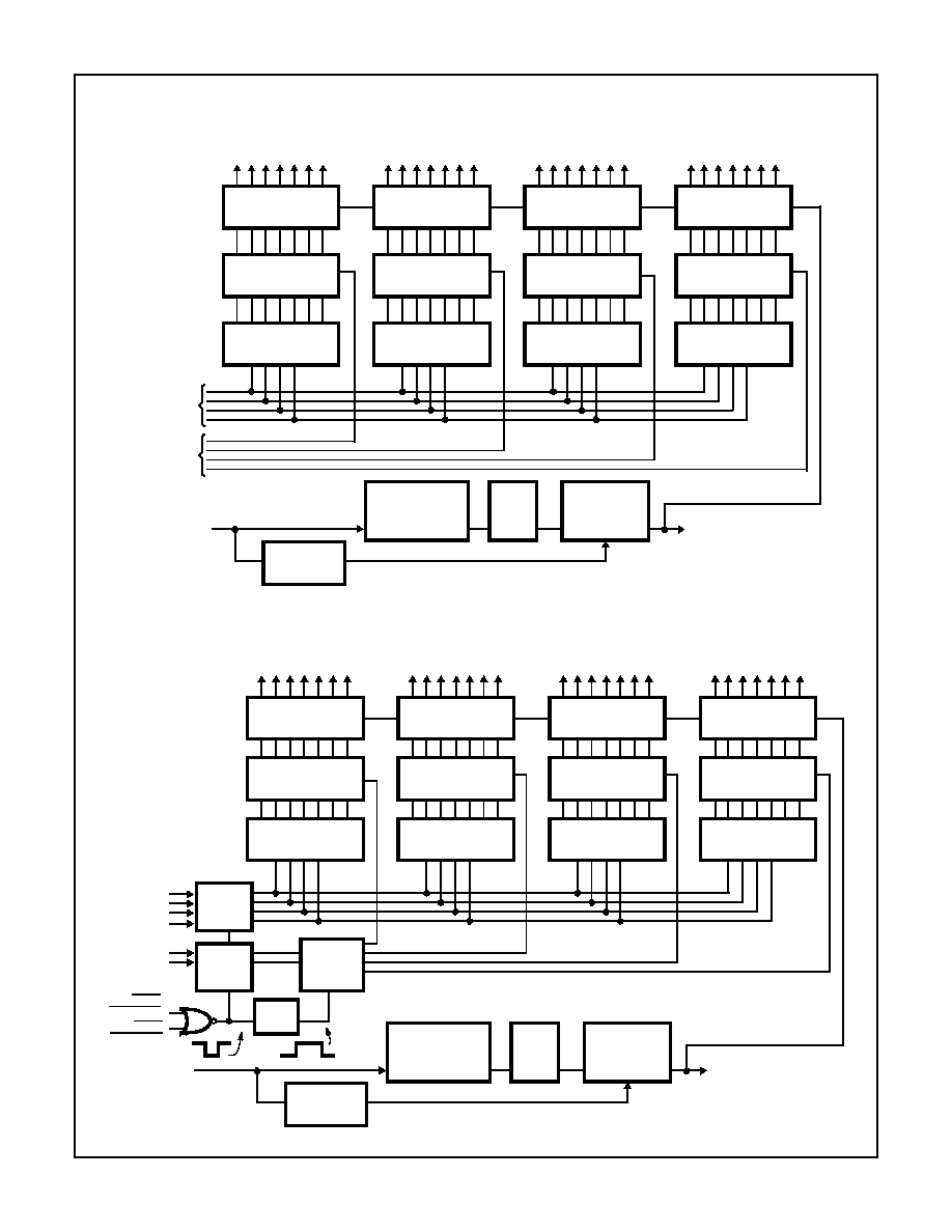
Functional Block Diagrams
ICM7211A
ICM7211AM
7 WIDE DRIVER
7 WIDE LATCH EN
PROGRAMMABLE
4 TO 7 DECODER
7 WIDE DRIVER
7 WIDE LATCH EN
PROGRAMMABLE
4 TO 7 DECODER
7 WIDE DRIVER
7 WIDE LATCH EN
PROGRAMMABLE
4 TO 7 DECODER
7 WIDE DRIVER
7 WIDE LATCH EN
PROGRAMMABLE
4 TO 7 DECODER
BLACKPLANE
DRIVER
ENABLE
OSCILLATOR
19kHz
FREE-RUNNING
˜
128
ENABLE
DIRECTOR
DATA
INPUTS
OSCILLATOR
DIGIT
SELECT
INPUTS
INPUT
BP INPUT/OUTPUT
D4
SEGMENT OUTPUTS
D3
SEGMENT OUTPUTS
D2
SEGMENT OUTPUTS
D1
SEGMENT OUTPUTS
7 WIDE DRIVER
7 WIDE LATCH EN
PROGRAMMABLE
4 TO 7 DECODER
7 WIDE DRIVER
7 WIDE LATCH EN
PROGRAMMABLE
4 TO 7 DECODER
7 WIDE DRIVER
7 WIDE LATCH EN
PROGRAMMABLE
4 TO 7 DECODER
7 WIDE DRIVER
7 WIDE LATCH EN
PROGRAMMABLE
4 TO 7 DECODER
D4
SEGMENT OUTPUTS
D3
SEGMENT OUTPUTS
D2
SEGMENT OUTPUTS
D1
SEGMENT OUTPUTS
2-BIT
DIGIT
ADRESS
INPUT
CHIP
CHIP
DATA
INPUTS
OSCILLATOR
INPUT
2 TO 4
DECODER
2-BIT
LATCH
ENABLE
4-BIT
LATCH
ENABLE
ONE
SHOT
SELECT 1
SELECT 2
BLACKPLANE
DRIVER
ENABLE
OSCILLATOR
19kHz
FREE-RUNNING
˜
128
ENABLE
DIRECTOR
BP INPUT/OUTPUT
ICM7211A

4
Absolute Maximum Ratings
Thermal Information
Supply Voltage (V
DD
- V
SS
) . . . . . . . . . . . . . . . . . . . . . . . . . . . . 6.5V
Input Voltage (Any Terminal) (Note 1) . . V
SS
- 0.3V to V
DD
, + 0.3V
Operating Conditions
Temperature Range . . . . . . . . . . . . . . . . . . . . . . . . . -40◊
o
C to 85
o
C
Thermal Resistance (Typical, Note 2)
JA
(
o
C/W)
PDIP Package . . . . . . . . . . . . . . . . . . . . . . . . . . . . .
60
MQFP Package . . . . . . . . . . . . . . . . . . . . . . . . . . . .
80
Maximum Junction Temperature . . . . . . . . . . . . . . . . . . . . . . . 150
o
C
Maximum Storage Temperature Range . . . . . . . . .-65◊
o
C to 150
o
C
Maximum Lead Temperature (Soldering, 10s) . . . . . . . . . . . . 300
o
C
(MQFP - Lead Tips Only)
CAUTION: Stresses above those listed in "Absolute Maximum Ratings" may cause permanent damage to the device. This is a stress only rating and operation
of the device at these or any other conditions above those indicated in the operational sections of this specification is not implied.
NOTES:
1. Due to the SCR structure inherent in the CMOS process, connecting any terminal to voltages greater than V
DD
or less than V
SS
may
cause destructive device latchup. For this reason, it is recommended that no inputs from external sources not operating on the same
power supply be applied to the device before its supply is established, and that in multiple supply systems, the supply to the ICM7211A
be turned on first.
2.
JA
is measured with the component mounted on an evaluation PC board in free air.
Electrical Specifications
PARAMETER
TEST CONDITIONS
MIN
TYP
MAX
UNITS
CHARACTERISTICS (LCD) V
DD
= 5V
±
10%, T
A
= 25
o
C, V
SS
= 0V Unless Otherwise Specified
Operating Supply Voltage Range (V
DD
- V
SS
), V
SUPPLY
3
5
6
V
Operating Current, I
DD
Test circuit, Display blank
-
10
50
µ
A
Oscillator Input Current, I
OSCI
Pin 36
-
±
2
±
10
µ
A
Segment Rise/Fall Time, t
r
, t
f
C
L
= 200pF
-
0.5
-
µ
s
Backplane Rise/Fall Time, t
r
, t
f
C
L
= 5000pF
-
1.5
-
µ
s
Oscillator Frequency, f
OSC
Pin 36 Floating
-
19
-
kHz
Backplane Frequency, f
BP
Pin 36 Floating
-
150
-
Hz
INPUT CHARACTERISTICS
Logical "1" Input Voltage, V
IH
4
-
-
V
Logical "0" Input Voltage, V
IL
-
-
1
V
Input Leakage Current, I
ILK
Pins 27-34
-
±
0.01
±
1
µ
A
Input Capacitance, C
lN
Pins 27-34
-
5
pF
BP/Brightness Input Leakage, I
BPLK
Measured at Pin 5 with Pin 36 at V
SS
-
±
0.01
±
1
µ
A
BP/Brightness Input Capacitance, C
BPI
All Devices
-
200
-
pF
AC CHARACTERISTICS - MULTIPLEXED INPUT CONFIGURATION
Digit Select Active Pulse Width, t
WH
Refer to Timing Diagrams
1
-
-
µ
s
Data Setup Time, t
DS
500
-
-
ns
Data Hold Time, t
DH
200
-
-
ns
Inter-Digit Select Time, t
IDS
2
-
-
µ
s
AC CHARACTERISTICS - MICROPROCESSOR INTERFACE
Chip Select Active Pulse Width, t
WL
Other Chip Select Either Held Active,
or Both Driven Together
200
-
-
ns
Data Setup Time, t
DS
100
-
-
ns
Data Hold Time, t
DH
10
0
-
ns
Inter-Chip Select Time, t
ICS
2
-
-
µ
s
ICM7211A
5
Input Definitions
In this table, V
DD
and V
SS
are considered to be normal operating input logic levels. Actual input low and high levels are
specified under Operating Characteristics. For lowest power consumption, input signals should swing over the full supply.
INPUT
DIP TERMINAL
CONDITIONS
FUNCTION
B0
27
V
DD
= Logical One
V
SS
= Logical Zero
Ones (Least Significant)
Data Input Bits
B1
28
V
DD
= Logical One
V
SS
= Logical Zero
Twos
B2
29
V
DD
= Logical One
V
SS
= Logical Zero
Fours
B3
30
V
DD
= Logical One
V
SS
= Logical Zero
Eights (Most Significant)
OSC
36
Floating or with External
Capacitor to V
DD
Oscillator Input
V
SS
Disables BP output devices, allowing segments to be synchronized to
an external signal input at the BP terminal (Pin 5).
Multiplexed-Binary Input Configuration
INPUT
TERMINAL
CONDITIONS
FUNCTION
D1
31
V
DD
= Active
V
SS
= Inactive
D1 Digit Select (Least Significant)
D2
32
D2 Digit Select
D3
33
D3 Digit Select
D4
34
D4 Digit Select (Most Significant)
Microprocessor Interface Input Configuration
INPUT
DESCRIPTION
DIP TERMINAL
CONDITIONS
FUNCTION
DA1
Digit Address
Bit 1 (LSB)
31
V
DD
= Logical One
V
SS
= Logical Zero
DA1 and DA2 serve as a 2-bit Digit Address Input
DA2, DA1 = 00 selects D4
DA2, DA1 = 01 selects D3
DA2, DA1 = 10 selects D2
DA2, DA1 = 11 selects D1
DA2
Digit Address
Bit 2 (MSB)
32
V
DD
= Logical One
V
SS
= Logical Zero
CS1
Chip Select 1
33
V
DD
= Inactive
V
SS
= Active
When both CS1 and CS2 are taken low, the data at the Data
and Digit Select code inputs are written into the input latches.
On the rising edge of either Chip Select, the data is decoded
and written into the output latches.
CS2
Chip Select 2
34
V
DD
= Inactive
V
SS
= Active
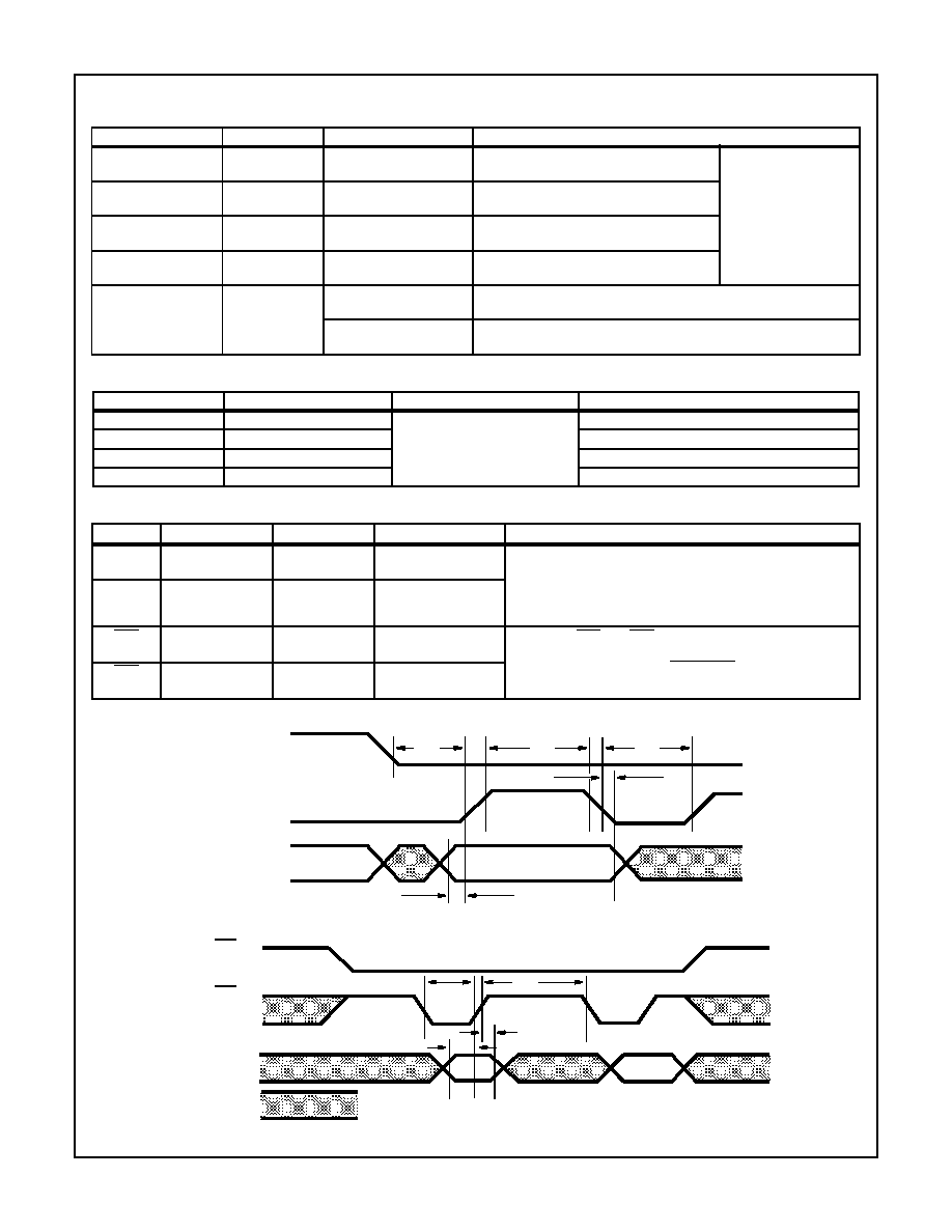
Timing Diagrams
FIGURE 1. MULTIPLEXED INPUT
FIGURE 2. MICROPROCESSOR INTERFACE INPUT
DIGIT SELECT
D
N-1
DIGIT SELECT
D
N
t
DH
t
DS
DATA VALID
D
N
DATA VALID
D
N-1
t
IDS
t
WH
t
IDS
CS1
(CS2)
CS2
(CS1)
DATA AND
DIGIT
ADDRESS
= DON'T CARE
t
DH
t
DS
t
WI
t
ICS
ICM7211A