9-12
August 1997
ICM7217
4-Digit LED Display,
Programmable Up/Down Counter
Features
∑ Four Decade, Presettable Up-Down Counter with
Parallel Zero Detect
∑ Settable Register with Contents Continuously
Compared to Counter
∑ Directly Drives Multiplexed 7 Segment Common
Anode or Common Cathode LED Displays
∑ On-Board Multiplex Scan Oscillator
∑ Schmitt Trigger On Count Input
∑ TTL Compatible BCD I/O Port, Carry/Borrow, Equal,
and Zero Outputs
∑ Display Blank Control for Lower Power Operation;
Quiescent Power Dissipation <5mW
∑ All Terminals Fully Protected Against Static Discharge
∑ Single 5V Supply Operation
Description
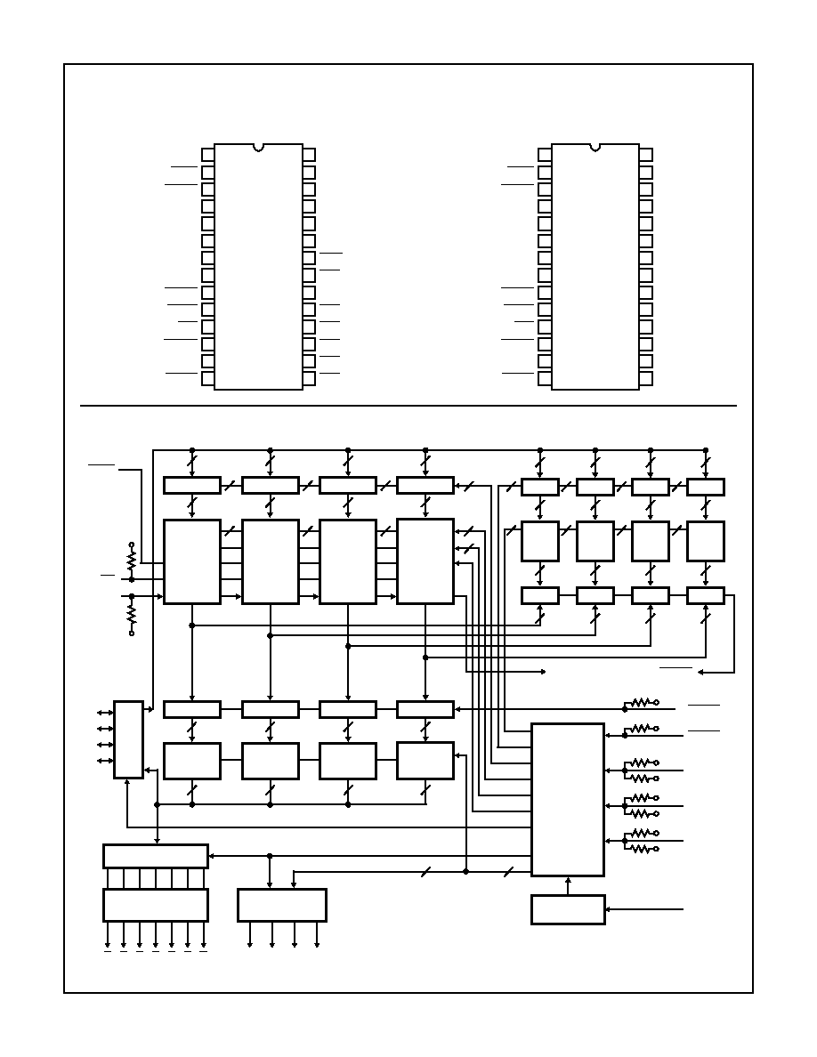
The ICM7217 is a four digit, presettable up/down counter with
an onboard presettable register continuously compared to the
counter. The ICM7217 is intended for use in hard-wired
applications where thumbwheel switches are used for loading
data, and simple SPDT switches are used for chip control.
This circuit provides multiplexed 7 segment LED display
outputs, with common anode or common cathode
configurations available. Digit and segment drivers are
provided to directly drive displays of up to 0.8 inch
character height (common anode) at a 25% duty cycle. The
frequency of the onboard multiplex oscillator may be
controlled with a single capacitor, or the oscillator may be
allowed to free run. Leading zeros can be blanked. The
data appearing at the 7 segment and BCD outputs is
latched; the content of the counter is transferred into the
latches under external control by means of the Store pin.
The ICM7217 (common anode) and ICM7217A (common
cathode) versions are decade counters, providing a
maximum count of 9999, while the ICM7217B (common
anode) and ICM7217C (common cathode) are intended for
timing purposes, providing a maximum count of 5959.
This circuit provides 3 main outputs; a CARRY/BORROW
output, which allows for direct cascading of counters, a
ZERO output, which indicates when the count is zero, and
an EQUAL output, which indicates when the count is equal
to the value contained in the register. Data is multiplexed to
and from the device by means of a three-state BCD I/O port.
The CARRY/BORROW, EQUAL, ZERO outputs, and the
BCD port will each drive one standard TTL load.
To permit operation in noisy environments and to prevent
multiple triggering with slowly changing inputs, the count
input is provided with a Schmitt trigger.
Input frequency is guaranteed to 2MHz, although the device will
typically run with f
IN
as high as 5MHz. Counting and comparing
(EQUAL output) will typically run 750kHz maximum.
Ordering Information
PART
NUMBER
TEMP. RANGE
(
o
C)
PACKAGE
DISPLAY DRIVER
TYPE
COUNT OPTION/
MAX COUNT
PKG. NO.
ICM7217AIPI
-25 to 85
28 Ld PDIP
Common Cathode
Decade/9999
E28.6
ICM7217CIPl
-25 to 85
28 Ld PDIP
Common Cathode
Timing/5959
E28.6
ICM7217IJI
-25 to 85
28 Ld CERDIP
Common Anode
Decade/9999
F28.6
lCM7217BlJl
-25 to 85
28 Ld CERDIP
Common Anode
Timing/5959
F28.6
File Number
3167.1
CAUTION: These devices are sensitive to electrostatic discharge; follow proper IC Handling Procedures.
http://www.intersil.com or 407-727-9207
|
Copyright
©
Intersil Corporation 1999
9-14
Absolute Maximum Ratings
Thermal Information
Supply Voltage (V
DD
- V
SS
) . . . . . . . . . . . . . . . . . . . . . . . . . . . . . 6V
Input Voltage (Any Terminal) . . . . . . . .(V
SS
- 0.3V) to (V
DD
+ 0.3V)
(Note 1)
Operating Conditions
Temperature Range . . . . . . . . . . . . . . . . . . . . . . . . . . -25
o
C to 85
o
C
Thermal Resistance (Typical, Note 2)
JA
(
o
C/W)
JC
(
o
C/W)
CERDIP Package . . . . . . . . . . . . . . . .
55
14
PDIP Package . . . . . . . . . . . . . . . . . . .
55
N/A
Maximum Junction Temperature
PDIP Package . . . . . . . . . . . . . . . . . . . . . . . . . . . . . . . . . . . 150
o
C
CERDIP Package . . . . . . . . . . . . . . . . . . . . . . . . . . . . . . . . 175
o
C
Maximum Storage Temperature Range . . . . . . . . . .-65
o
C to 150
o
C
Maximum Lead Temperature (Soldering, 10s) . . . . . . . . . . . . 300
o
C
CAUTION: Stresses above those listed in "Absolute Maximum Ratings" may cause permanent damage to the device. This is a stress only rating and operation
of the device at these or any other conditions above those indicated in the operational sections of this specification is not implied.
NOTES:
1. Due to the SCR structure inherent in the CMOS process used to fabricate these devices, connecting any terminal to a voltage greater
than V
DD
or less than V
SS
may cause destructive device latchup. For this reason it is recommended that the power supply to the device
be established before any inputs are applied and that in multiple systems the supply to the ICM7217 be turned on first.
2.
JA
is measured with the component mounted on an evaluation PC board in free air.
Electrical Specifications
V
DD
= 5V, V
SS
= 0V, T
A
= 25
o
C, Display Diode Drop 1 .7V, Unless Otherwise Specified
PARAMETER
TEST CONDITIONS
MIN
TYP
MAX
UNIT
Supply Current
(Lowest Power Mode), IDD (7217)
Display Off, LC, DC, UP/DN,
ST, RS, BCD I/O Floating or at V
DD
(Note 1)
-
350
500
µ
A
Supply Current, OPERATING, I
OP
Common Anode, Display On, all "8's"
140
200
-
mA
Supply Current, OPERATING, I
OP
Common Cathode, Display On, all "8's"
50
100
-
mA
V
SUPPLY
, V
DD
4.5
5
5.5
V
Digit Driver Output Current, I
DIG
Common Anode, V
OUT
= V
DD
- 2.0V
140
200
-
mA
PEAK
SEGment Driver
Output Current, ISEG
Common Anode, V
OUT
= +1.5V
20
35
-
mA
PEAK
Digit Driver, Output Current, I
DIG
Common Cathode, V
OUT
= +1.0V
-50
-75
-
mA
PEAK
SEGment Driver
Output Current, ISEG
Common Cathode V
OUT
= V
DD
- 2V
-9
-12.5
-
mA
PEAK
ST, RS, UP/DN Input
Pullup Current, IP
V
IN
= V
DD
- 2V (Note 1)
5
25
-
µ
A
3 Level Input Impendance, ZIN
40
-
350
k
BCD I/O Input, High Voltage
VBIH
ICM7217 Common Anode (Note 2)
1.5
-
-
V
ICM7217 Common Cathode (Note 2)
4.40
-
-
V
BCD I/O Input, Low Voltage
VBIL
ICM7217 Common Anode (Note 2)
-
-
0.60
V
ICM7217 Common Cathode (Note 2)
-
-
3.2V
V
BCD I/O Input, Pullup Current
IBPU
ICM7217 Common Cathode V
IN
= V
DD
- 2V
(Note 2)
5
25
-
µ
A
BCD I/O Input
Pulldown Current, IBPD
ICM7217 Common Anode V
IN
= +2V (Note 2)
5
25
-
µ
A
BCD I/O, ZERO, EQUAL Outputs
Output High Voltage, VOH
I
OH
= -100
µ
A
3.5
-
-
V
BCD I/O, CARRY/BORROW
ZERO, EQUAL Outputs
Output Low Voltage, V
OL
I
OL
= 1.6mA
-
-
0.4
V
Count Input Frequency, f
IN
-20
o
C to 70
o
C
-
5
-
MHz
Guaranteed
0
-
2
MHz
Count Input Threshold, VTH
(Note 3)
-
2
-
V
Count Input Hysteresis, VHYS
(Note 3)
-
0.5
-
V
Count Input LO, VCIL
-
-
0.40
V
Count Input HI, VCIH
3.5
-
-
V
Display Scan
Oscillator Frequency, f
DS
Free-running (SCAN Terminal Open Circuit)
-
2.5
10
kHz
ICM7217
9-15
Switching Specifications
V
DD
= 5V, V
SS
= 0V, T
A
= 25
o
C
PARAMETER
MIN
TYP
MAX
UNIT
UP/DOWN Setup Time, t
UCS
300
-
-
ns
UP/DOWN Hold Time, t
UCH
1500
750
-
ns
COUNT Pulse Width High, t
CWH
250
100
-
ns
COUNT Pulse Width Low, t
CWI
250
100
-
ns
COUNT to CARRY/BORROW Delay, t
CB
-
750
-
ns
CARRY/BORROW Pulse Width t
BW
-
100
-
ns
COUNT to EQUAL Delay, t
CE
-
500
-
ns
COUNT to ZERO Delay, t
CZ
-
300
-
ns
RESET Pulse Width, t
RST
1000
500
-
ns
NOTES:
1. In the ICM7217 the UP/DOWN, STORE, RESET and the BCD I/O as inputs have pullup or pulldown devices which consume power when
connected to the opposite supply. Under these conditions, with the display off, the device will consume typically 750
µ
A.
2. These voltages are adjusted to allow the use of thumbwheel switches for the ICM7217. Note that a high level is taken as an input logic
zero for ICM7217 common-cathode versions.
3. Parameters not tested (Guaranteed by Design).
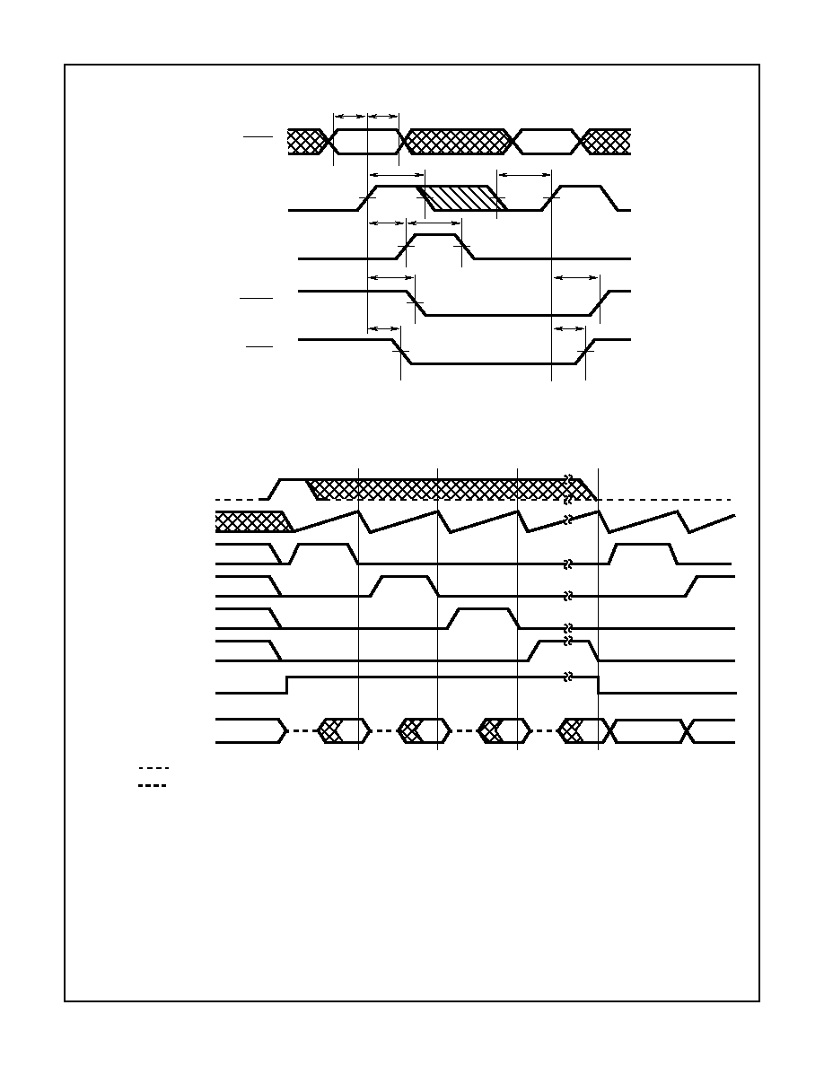
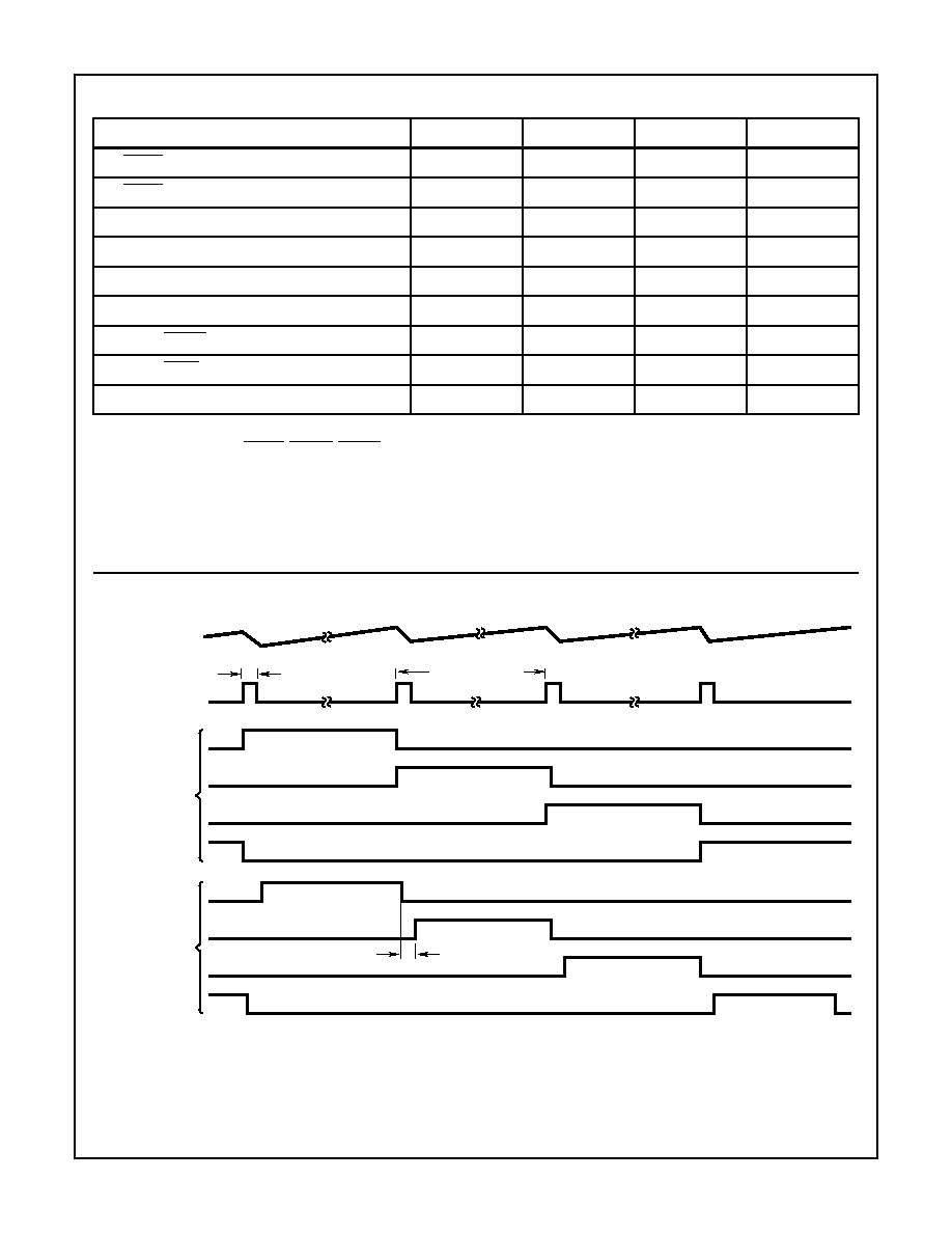
Timing Waveforms
FIGURE 1. MULTIPLEX TIMING
10
µ
s TYP
400
µ
s TYP
FREE-RUNNING
FREE-RUNNING
INTERDIGIT BLANK
D4
D3
D2
D1
SCAN
INTERNAL OSC
OUTPUT
INTERNAL
(BCD AND
SEGMENT
ENABLE)
INTERNAL
(COMMON
ANODE
DIGIT
STROBES)
D4
D3
D2
D1
ICM7217