 | –≠–ª–µ–∫—Ç—Ä–æ–Ω–Ω—ã–π –∫–æ–º–ø–æ–Ω–µ–Ω—Ç: ICM7217B | –°–∫–∞—á–∞—Ç—å:  PDF PDF  ZIP ZIP |
1
Æ
July 2001
ICM7217
4-Digit LED Display,
Programmable Up/Down Counter
Features
∑ Four Decade, Presettable Up-Down Counter with
Parallel Zero Detect
∑ Settable Register with Contents Continuously
Compared to Counter
∑ Directly Drives Multiplexed 7 Segment Common
Anode or Common Cathode LED Displays
∑ On-Board Multiplex Scan Oscillator
∑ Schmitt Trigger On Count Input
∑ TTL Compatible BCD I/O Port, Carry/Borrow, Equal,
and Zero Outputs
∑ Display Blank Control for Lower Power Operation;
Quiescent Power Dissipation <5mW
∑ All Terminals Fully Protected Against Static Discharge
∑ Single 5V Supply Operation
Description
The ICM7217 is a four digit, presettable up/down counter with
an onboard presettable register continuously compared to the
counter. The ICM7217 is intended for use in hard-wired
applications where thumbwheel switches are used for loading
data, and simple SPDT switches are used for chip control.
This circuit provides multiplexed 7 segment LED display
outputs, with common anode or common cathode
configurations available. Digit and segment drivers are
provided to directly drive displays of up to 0.8 inch
character height (common anode) at a 25% duty cycle. The
frequency of the onboard multiplex oscillator may be
controlled with a single capacitor, or the oscillator may be
allowed to free run. Leading zeros can be blanked. The
data appearing at the 7 segment and BCD outputs is
latched; the content of the counter is transferred into the
latches under external control by means of the Store pin.
The ICM7217 (common anode) and ICM7217A (common
cathode) versions are decade counters, providing a
maximum count of 9999, while the ICM7217B (common
anode) and ICM7217C (common cathode) are intended for
timing purposes, providing a maximum count of 5959.
This circuit provides 3 main outputs; a CARRY/BORROW
output, which allows for direct cascading of counters, a
ZERO output, which indicates when the count is zero, and
an EQUAL output, which indicates when the count is equal
to the value contained in the register. Data is multiplexed to
and from the device by means of a three-state BCD I/O port.
The CARRY/BORROW, EQUAL, ZERO outputs, and the
BCD port will each drive one standard TTL load.
To permit operation in noisy environments and to prevent
multiple triggering with slowly changing inputs, the count
input is provided with a Schmitt trigger.
Input frequency is guaranteed to 2MHz, although the device will
typically run with f
IN
as high as 5MHz. Counting and comparing
(EQUAL output) will typically run 750kHz maximum.
Part Number Information
PART
NUMBER
TEMP. RANGE
(
o
C)
PACKAGE
DISPLAY DRIVER
TYPE
COUNT OPTION/
MAX COUNT
PKG. NO.
ICM7217AIPI
-25 to 85
28 Ld PDIP
Common Cathode
Decade/9999
E28.6
ICM7217CIPl
-25 to 85
28 Ld PDIP
Common Cathode
Timing/5959
E28.6
ICM7217IJI
-25 to 85
28 Ld CERDIP
Common Anode
Decade/9999
F28.6
lCM7217BlJl
-25 to 85
28 Ld CERDIP
Common Anode
Timing/5959
F28.6
File Number
3167.3
CAUTION: These devices are sensitive to electrostatic discharge; follow proper IC Handling Procedures.
1-888-INTERSIL or 321-724-7143
|
Intersil (and design) is a registered trademark of Intersil Americas Inc.
Copyright © Intersil Americas Inc. 2002. All Rights Reserved
FOR A
POSSIB
LE SUB
STITUT
E PROD
UCT
contac
t our Te
chnical
Suppo
rt Cent
er at
1-888-IN
TERSIL
or www
.intersi
l.com/ts
c
OBSOL
ETE PR
ODUCT
2
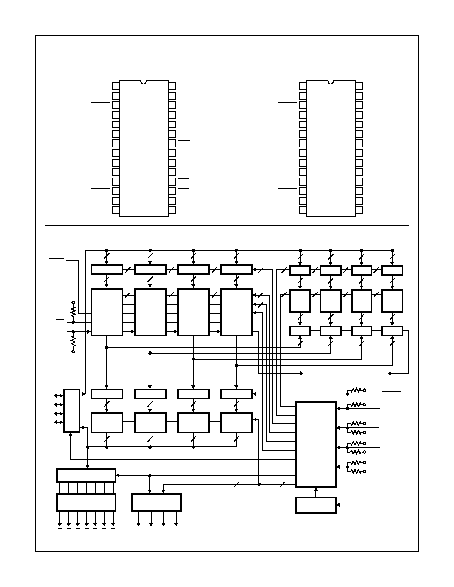
Pinouts
Functional Block Diagram
ICM7217 (CERDIP)
COMMON ANODE
TOP VIEW
ICM7217 (PDIP)
COMMON CATHODE
TOP VIEW
CARRY/BORROW
ZERO
EQUAL
BCD I/O 8s
BCD I/O 4s
BCD I/O 2s
BCD I/O 1s
COUNT INPUT
STORE
UP/DOWN
LOAD REGISTER/OFF
LOAD COUNTER/I/O OFF
SCAN
RESET
D1
D3
D4
V
DD
DISPLAY CONT.
SEG
b
SEG
e
SEG
f
SEG
d
SEG
a
SEG
c
D2
SEG
g
V
SS
28
27
26
25
24
23
22
21
20
19
18
17
16
15
1
2
3
4
5
6
7
8
9
10
11
12
13
14
ICM7217
ICM7217B
CARRY/BORROW
ZERO
EQUAL
BCD I/O 8s
BCD I/O 4s
BCD I/O 2s
BCD I/O 1s
COUNT INPUT
STORE
UP/DOWN
LOAD REGISTER/OFF
LOAD COUNTER/I/O OFF
SCAN
RESET
SEG
d
SEG
f
SEG
c
V
DD
SEG
a
SEG
g
V
SS
D1
D2
D3
D4
SEG
b
SEG
e
DISPLAY CONT.
28
27
26
25
24
23
22
21
20
19
18
17
16
15
1
2
3
4
5
6
7
8
9
10
11
12
13
14
ICM7217A
ICM7217C
T.G.
D4
10
RS
ZERO
U/D
CL CARRY
T.G.
LATCH
MUX
4
4
4
4
T.G.
D2
10
RS
ZERO
U/D
CL CARRY
T.G.
LATCH
MUX
4
4
4
4
T.G.
D3
10
RS
ZERO
U/D
CL CARRY
T.G.
LATCH
MUX
4
4
4
4
T.G.
D1
10
RS
ZERO
U/D
CL CARRY
T.G.
LATCH
MUX
4
4
4
4
1
2
3
4
T.G.
4
4
D1
COMP.
4
REG.
1
2
3
4
1
2
3
4
1
2
3
4
4
4
T.G.
4
4
D2
COMP.
4
REG.
4
T.G.
4
4
D3
COMP.
4
REG.
4
T.G.
4
4
D4
COMP.
4
REG.
4
BDC
I/O
8
s
4
s
2
s
1
s
ZERO
UP/DN
COUNT
V
DD
V
SS
SEGMENT DECODER
SEGMENT DRIVERS
(7)
DIGIT DRIVERS
(4)
A
D4 D3 D2 D1
DISPLAY BLANK + OFF
G
B C D E F
MUX.
OSCILLATOR
MUX. I/O
AND
DISPLAY
CONTROL
LOGIC
4
4
DIGIT MUX
SCAN
DISPLAY
LOAD
LOAD
RESET
STORE
EQUAL
CARRY/BARROW
CONTROL
REGISTER
COUNTER
L.R.
L.C.
RESET
BCD I/O INPUTS
COM. ANODE: PULL DOWN
COM. CATHODE: PULL UP
V
DD
V
DD
V
DD
V
SS
V
DD
V
SS
V
DD
V
SS
ICM7217
3
Absolute Maximum Ratings
Thermal Information
Supply Voltage (V
DD
- V
SS
) . . . . . . . . . . . . . . . . . . . . . . . . . . . . . 6V
Input Voltage (Any Terminal) . . . . . . . . (V
SS
- 0.3V) to (V
DD
+ 0.3V)
(Note 1)
Operating Conditions
Temperature Range . . . . . . . . . . . . . . . . . . . . . . . . . . -25
o
C to 85
o
C
Thermal Resistance (Typical, Note 2)
JA
(
o
C/W)
JC
(
o
C/W)
CERDIP Package . . . . . . . . . . . . . . . .
55
14
PDIP Package . . . . . . . . . . . . . . . . . . .
55
N/A
Maximum Junction Temperature
PDIP Package . . . . . . . . . . . . . . . . . . . . . . . . . . . . . . . . . . . 150
o
C
CERDIP Package . . . . . . . . . . . . . . . . . . . . . . . . . . . . . . . . 175
o
C
Maximum Storage Temperature Range . . . . . . . . . . -65
o
C to 150
o
C
Maximum Lead Temperature (Soldering, 10s) . . . . . . . . . . . . 300
o
C
CAUTION: Stresses above those listed in "Absolute Maximum Ratings" may cause permanent damage to the device. This is a stress only rating and operation
of the device at these or any other conditions above those indicated in the operational sections of this specification is not implied.
NOTES:
1. Due to the SCR structure inherent in the CMOS process used to fabricate these devices, connecting any terminal to a voltage greater
than V
DD
or less than V
SS
may cause destructive device latchup. For this reason it is recommended that the power supply to the device
be established before any inputs are applied and that in multiple systems the supply to the ICM7217 be turned on first.
2.
JA
is measured with the component mounted on an evaluation PC board in free air.
Electrical Specifications
V
DD
= 5V, V
SS
= 0V, T
A
= 25
o
C, Display Diode Drop 1 .7V, Unless Otherwise Specified
PARAMETER
TEST CONDITIONS
MIN
TYP
MAX
UNIT
Supply Current
(Lowest Power Mode), IDD (7217)
Display Off, LC, DC, UP/DN,
ST, RS, BCD I/O Floating or at V
DD
(Note 1)
-
350
500
µA
Supply Current, OPERATING, I
OP
Common Anode, Display On, all "8's"
140
200
-
mA
Supply Current, OPERATING, I
OP
Common Cathode, Display On, all "8's"
50
100
-
mA
V
SUPPLY
, V
DD
4.5
5
5.5
V
Digit Driver Output Current, I
DIG
Common Anode, V
OUT
= V
DD
- 2.0V
140
200
-
mA
PEAK
SEGment Driver
Output Current, ISEG
Common Anode, V
OUT
= +1.5V
20
35
-
mA
PEAK
Digit Driver, Output Current, I
DIG
Common Cathode, V
OUT
= +1.0V
-50
-75
-
mA
PEAK
SEGment Driver
Output Current, ISEG
Common Cathode V
OUT
= V
DD
- 2V
-9
-12.5
-
mA
PEAK
ST, RS, UP/DN Input
Pullup Current, IP
V
IN
= V
DD
- 2V (Note 1)
5
25
-
µA
3 Level Input Impendance, ZIN
40
-
350
k
BCD I/O Input, High Voltage
VBIH
ICM7217 Common Anode (Note 2)
1.5
-
-
V
ICM7217 Common Cathode (Note 2)
4.40
-
-
V
BCD I/O Input, Low Voltage
VBIL
ICM7217 Common Anode (Note 2)
-
-
0.60
V
ICM7217 Common Cathode (Note 2)
-
-
3.2V
V
BCD I/O Input, Pullup Current
IBPU
ICM7217 Common Cathode V
IN
= V
DD
- 2V
(Note 2)
5
25
-
µA
BCD I/O Input
Pulldown Current, IBPD
ICM7217 Common Anode V
IN
= +2V (Note 2)
5
25
-
µA
BCD I/O, ZERO, EQUAL Outputs
Output High Voltage, VOH
I
OH
= -100
µA
3.5
-
-
V
BCD I/O, CARRY/BORROW
ZERO, EQUAL Outputs
Output Low Voltage, V
OL
I
OL
= 1.6mA
-
-
0.4
V
Count Input Frequency, f
IN
-20
o
C to 70
o
C
-
5
-
MHz
Guaranteed
0
-
2
MHz
Count Input Threshold, VTH
(Note 3)
-
2
-
V
Count Input Hysteresis, VHYS
(Note 3)
-
0.5
-
V
Count Input LO, VCIL
-
-
0.40
V
Count Input HI, VCIH
3.5
-
-
V
ICM7217
4
Display Scan
Oscillator Frequency, f
DS
Free-running (SCAN Terminal Open Circuit)
-
2.5
10
kHz
Switching Specifications
V
DD
= 5V, V
SS
= 0V, T
A
= 25
o
C
PARAMETER
MIN
TYP
MAX UNIT
UP/DOWN Setup Time, t
UCS
300
-
-
ns
UP/DOWN Hold Time, t
UCH
1500
750
-
ns
COUNT Pulse Width High, t
CWH
250
100
-
ns
COUNT Pulse Width Low, t
CWI
250
100
-
ns
COUNT to CARRY/BORROW Delay, t
CB
-
750
-
ns
CARRY/BORROW Pulse Width t
BW
-
100
-
ns
COUNT to EQUAL Delay, t
CE
-
500
-
ns
COUNT to ZERO Delay, t
CZ
-
300
-
ns
RESET Pulse Width, t
RST
1000
500
-
ns
NOTES:
1. In the ICM7217 the UP/DOWN, STORE, RESET and the BCD I/O as inputs have pullup or pulldown devices which consume power when
connected to the opposite supply. Under these conditions, with the display off, the device will consume typically 750
µA.
2. These voltages are adjusted to allow the use of thumbwheel switches for the ICM7217. Note that a high level is taken as an input logic
zero for ICM7217 common-cathode versions.
3. Parameters not tested (Guaranteed by Design).
Electrical Specifications
V
DD
= 5V, V
SS
= 0V, T
A
= 25
o
C, Display Diode Drop 1 .7V, Unless Otherwise Specified
PARAMETER
TEST CONDITIONS
MIN
TYP
MAX
UNIT
ICM7217

5
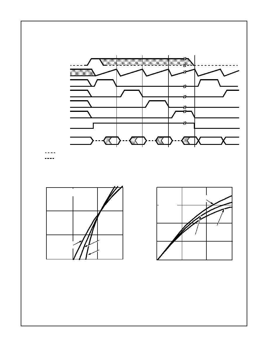
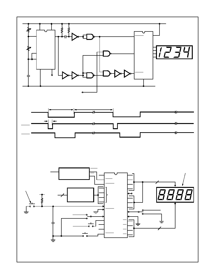
Timing Waveforms
FIGURE 1. MULTIPLEX TIMING
FIGURE 2. COUNT AND OUTPUTS TIMING
10
µs TYP
400
µs TYP
FREE-RUNNING
FREE-RUNNING
INTERDIGIT BLANK
D4
D3
D2
D1
SCAN
INTERNAL OSC
OUTPUT
INTERNAL
(BCD AND
SEGMENT
ENABLE)
INTERNAL
(COMMON
ANODE
DIGIT
STROBES)
D4
D3
D2
D1
CARRY/BORROW
ZERO
EQUAL
COUNT INPUT
UP/DOWN
t
UCH
t
CWH
t
BW
t
CEL
t
CZL
t
CZH
t
CEH
t
CWL
t
CB
t
UCS
ICM7217
6
FIGURE 3. BCD I/O AND LOADING TIMING
Timing Waveforms
D4
D3
D2
D1
SCAN
INPUT
OUTPUT
INTERNAL
OPERATING
MODE
BCD I/O
D
N
OUT
LOAD COUNTER
(OR LOAD REGISTER)
D4
IN
D3
IN
D2
IN
D1
IN
D4 OUT
D3 OUT
COUNT INHIBITED IF
LOAD COUNTER
= HIGH IMPEDANCE
= THREE-STATE W/PULLDOWN
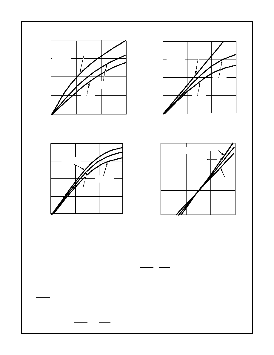
Typical Performance Curves
FIGURE 4. TYPICAL IDIG vs V+
FIGURE 5. TYPICAL ISEG vs V
OUT
V
DD
- V
OUT
(V)
IDIG
(
m
A)
300
200
100
0
0
1
2
3
4.5
V
DD
6V
85
o
C
25
o
C
-20
o
C
ICM7217
ICM7217B
V
OUT
(V)
0
1
2
3
60
40
20
0
80
IS
E
G
(
m
A)
V+ = 5.5V
V+ = 5V
V+ = 4.5V
T
A
= 25
o
C
ICM7217
ICM7217B
ICM7217
7
Detailed Description
Control Outputs
The CARRY/BORROW output is a positive going pulse
occurring typically 500ns after the positive going edge of the
COUNT INPUT. It occurs when the counter is clocked from
9999 to 0000 when counting up and from 0000 to 9999 when
counting down. This output allows direct cascading of
counters. The CARRY/BORROW output is not valid during
load counter and reset operation. When the count is 6000 or
higher, a reset generates a CARRY/BORROW pulse.
The EQUAL output assumes a negative level when the
contents of the counter and register are equal.
The ZERO output assumes a negative level when the
content of the counter is 0000.
The CARRY/BORROW, EQUAL and ZERO outputs will
drive a single TTL load over the full range of supply voltage
and ambient temperature; for a logic zero, these outputs will
sink 1.6mA at 0.4V and for a logic one, the outputs will
source >60
µA. A 10k pull-up resistor to V
DD
on the
EQUAL or ZERO outputs is recommended for highest speed
operation, and on the CARRY/BORROW output when it is
being used for cascading. Figure 2 shows control outputs
timing diagram.
Display Outputs and Control
The Digit and SEGment drivers provide a decoded
7-segment display system, capable of directly driving com-
mon anode LED displays at typical peak currents of
35mA/seg. This corresponds to average currents of
8mA/seg at 25% multiplex duty cycle. For the common cath-
ode versions, peak segment currents are 12.5mA, corre-
FIGURE 6. TYPICAL ISEG vs V
OUT
FIGURE 7. TYPICAL IDIGIT vs V
OUT
FIGURE 8. TYPICAL IDIGIT vs V
OUT
FIGURE 9. TYPICAL ISEG vs V
DD
- V
OUT
Typical Performance Curves
V
OUT
(V)
0
1
2
3
60
40
20
0
80
IS
E
G
(
m
A)
85
o
C
25
o
C
-20
o
C
V+ = 5V
ICM7217
ICM7217B
85
o
C
25
o
C
-20
o
C
V+ = 5V
V
OUT
(V)
IDIG
IT
(
m
A)
150
100
50
0
200
0
1
2
3
ICM7217A
ICM7217C
V
OUT
(V)
0
1
2
3
V+ = 5.5V
V+ = 5V
V+ = 4.5V
T
A
= 25
o
C
IDIG
IT
(
m
A)
100
50
0
150
200
ICM7217A
ICM7217C
V
DD
- V
OUT
(V)
0
1
2
3
30
20
10
0
IS
E
G
(
m
A)
-20
o
C
25
o
C
85
o
C
4.5
V
DD
- V
SS
6V
ICM7217A
ICM7217C
ICM7217
8
sponding to average segment currents of 3.1mA. Figure 1
shows the multiplex timing. The DISPLAY pin controls the
display output using three level logic. The pin is self-biased
to a voltage approximately
1
/
2
(V
DD
); this corresponds to
normal operation. When this pin is connected to V
DD
, the
segments are disabled and when connected to V
SS
, the
leading zero blanking feature is inhibited. For normal opera-
tion (display on with leading zero blanking) the pin should be
left open. The display may be controlled with a 3 position
SPDT switch; see Test Circuit.
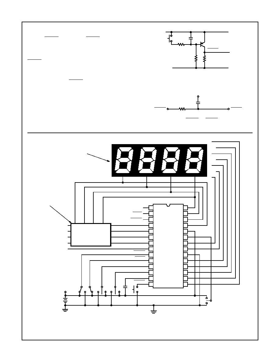
Multiplex SCAN Oscillator
The on-board multiplex scan oscillator has a nominal free-
running frequency of 2.5kHz. This may be reduced by the
addition of a single capacitor between the SCAN pin and the
positive supply. Capacitor values and corresponding nomi-
nal oscillator frequencies, digit repetition rates, and loading
times are shown in Table 1.
The internal oscillator output has a duty cycle of
approximately 25:1, providing a short pulse occurring at the
oscillator frequency. This pulse clocks the four-state counter
which provides the four multiplex phases. The short pulse
width is used to delay the digit driver outputs, thereby provid-
ing inter-digit blanking which prevents ghosting. The digits
are scanned from MSD (D4) to LSD (D1). See Figure 1 for
the display digit multiplex timing.
During load counter and load register operations, the
multiplex oscillator is disconnected from the SCAN input and
is allowed to free-run. In all other conditions, the oscillator
may be directly overdriven to about 20kHz, however the
external oscillator signal should have the same duty cycle as
the internal signal, since the digits are blanked during the
time the external signal is at a positive level (see Figure 1).
To insure proper leading zero blanking, the interdigit blank-
ing time should not be less than about 2
µs. Overdriving the
oscillator at less than 200Hz may cause display flickering.
The display brightness may be altered by varying the duty
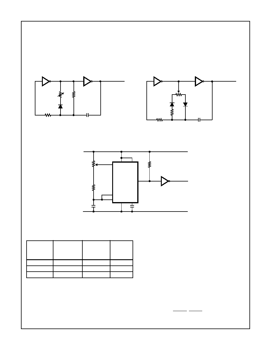
cycle. Figure 10 shows several variable-duty-cycle oscilla-
tors suitable for brightness control at the ICM7217 SCAN
input. The inverters should be CMOS CD4000 series and
the diodes may be any inexpensive device such as lN914.
Counting Control, STORE, RESET
As shown in Figure 2, the counter is incremented by the
FIGURE 10A.
FIGURE 10B.
FIGURE 10C.
FIGURE 10. BRIGHTNESS CONTROL CIRCUITS
R2
20k
1M
0.01
µF
C
SCAN INPUT
ICM7217
R1
10k
1M
0.01
µF
SCAN INPUT
ICM7217
500
500
3k
0.05
µF
SCAN INPUT
ICM7217
10k
200
0.05
µF
7
4
8
3
2
6
1
8s
ICM7555
0V
V
DD
= 5V
TABLE 1. ICM7217 MULTIPLEXED RATE CONTROL
SCAN
CAPACITOR
NOMINAL
OSCILLATOR
FREQUENCY
DIGIT
REPETITION
RATE
SCAN
CYCLE
TIME
(4 DIGITS)
None
2.5kHz
625Hz
1.6ms
20pF
1.25kHz
300Hz
3.2ms
90pF
600Hz
150Hz
8ms
ICM7217
9
rising edge of the COUNT INPUT signal when UP/DOWN is
high. It is decremented when UP/DOWN is low. A Schmitt
trigger on the COUNT INPUT provides hysteresis to prevent
double triggering on slow rising edges and permits operation
in noisy environments. The COUNT INPUT is inhibited dur-
ing reset and load counter operations.
The STORE pin controls the internal latches and
consequently the signals appearing at the 7-Segment and
BCD outputs. Bringing the STORE pin low transfers the con-
tents of the counter into the latches.
The counter is asynchronously reset to 0000 by bringing the
RESET pin low. The circuit performs the reset operation by
forcing the BCD input lines to zero, and "presetting" all four
decades of counter in parallel. This affects register loading; if
LOAD REGISTER is activated when the RESET input is low,
the register will also be set to zero. The STORE, RESET and
UP/DOWN pins are provided with pullup resistors of approx-
imately 75k
.
BCD I/O Pins
The BCD I/O port provides a means of transferring data to
and from the device. The ICM7217 versions can multiplex
data into the counter or register via thumbwheel switches,
depending on inputs to the LOAD COUNTER or LOAD
REGISTER pins; (see below). When functioning as outputs,
the BCD I/O pins will drive one standard TTL load. Common
anode versions have internal pull down resistors and com-
mon cathode versions have internal pull up resistors on the
four BCD I/O lines when used as inputs.
LOADing the COUNTER and REGISTER
The BCD I/O pins, the LOAD COUNTER (LC), and LOAD
REGISTER (LR) pins combine to provide presetting and
compare functions. LC and LR are 3-level inputs, being self-
biased at approximately
1
/
2
V
DD
for normal operation. With
both LC and LR open, the BCD I/O pins provide a multi-
plexed BCD output of the latch contents, scanned from MSD
to LSD by the display multiplex.
When either the LOAD COUNTER (Pin 12) or LOAD
REGISTER (Pin 11) is taken low, the drivers are turned off
and the BCD pins become high-impedance inputs. When LC
is connected to V
DD
, the count input is inhibited and the lev-
els at the BCD pins are multiplexed into the counter. When
LR is connected to V
DD
, the levels at the BCD pins are mul-
tiplexed into the register without disturbing the counter.
When both are connected to V
DD
, the count is inhibited and
both register and counter will be loaded.
The LOAD COUNTER and LOAD REGISTER inputs are
edge-triggered, and pulsing them high for 500ns at room
temperature will initiate a full sequence of data entry cycle
operations (see Figure 3). When the circuit recognizes that
either or both of the LC or LR pins input is high, the multiplex
oscillator and counter are reset (to D4). The internal
oscillator is then disconnected from the SCAN pin and the
preset circuitry is enabled. The oscillator starts and runs with
a frequency determined by its internal capacitor, (which may
vary from chip to chip). When the chip finishes a full 4-digit
multiplex cycle (loading each digit from D4 to D3 to D2 to D1
in turn), it again samples the LOAD REGISTER and LOAD
COUNTER inputs. If either or both is still high, it repeats the
load cycle, if both are floating or low, the oscillator is
reconnected to the SCAN pin and the chip returns to normal
operation. Total load time is digit "on" time multiplied by 4. lf
the Digit outputs are used to strobe the BCD data into the
BCD I/O inputs, the input must be synchronized to the
appropriate digit (Figure 3). Input data must be valid at the
trailing edge of the digit output.
When LR is connected to GROUND, the oscillator is
inhibited, the BCD I/O pins go to the high impedance state,
and the segment and digit drivers are turned off. This allows
the display to be used for other purposes and minimizes
power consumption. In this display off condition, the circuit
will continue to count, and the CARRY/BORROW, EQUAL,
ZERO, UP/DOWN, RESET and STORE functions operate
as normal. When LC is connected to ground, the BCD I/O
pins are forced to the high impedance state without disturb-
ing the counter or register. See "Control Input Definitions"
(Table 2) for a list of the pins that function as three-state self-
biased inputs and their respective operations.
Note that the ICM7217 and ICM7217B have been designed
to drive common anode displays. The BCD inputs are high
true, as are the BCD outputs.
INPUT
OUTPUT
INPUT
OUTPUT
High
High
High
Disconnected
Low
Disconnected
Low
High
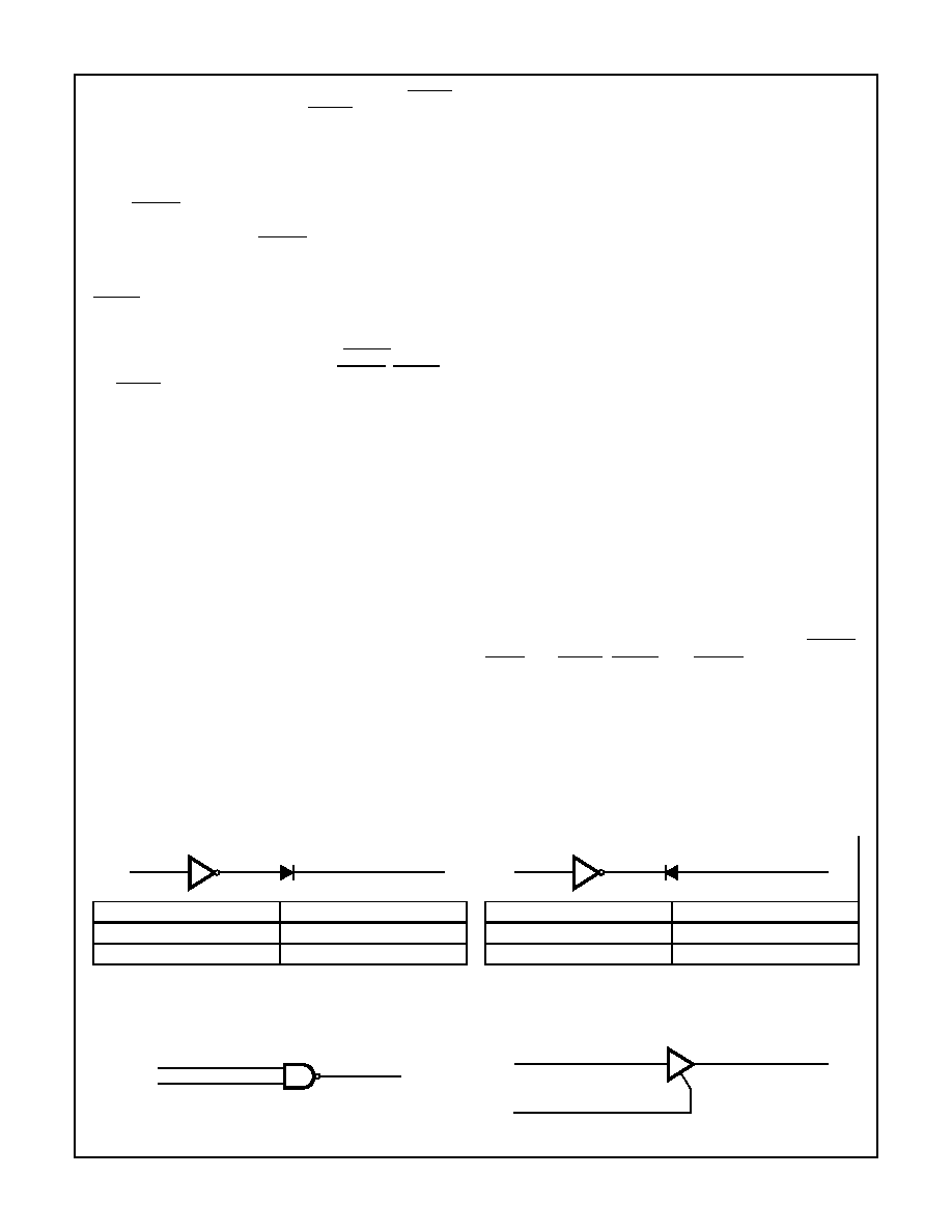
FIGURE 11A. CMOS INVERTER
FIGURE 11B. CMOS INVERTER
INPUT
CD4069
1N4148
OUTPUT
INPUT
CD4069
OUTPUT
1N4148
INPUT A
CD74HC03
OUTPUT
INPUT B
INPUT A
CD4502B
OUTPUT
INPUT B
ICM7217
10
INPUT B
INPUT A
OUTPUT
INPUT B
INPUT A
OUTPUT
High
High
Low
High
High
Disconnected
High
Low
Disconnected
High
Low
Disconnected
Low
High
Disconnected
Low
High
High
Low
Low
Disconnected
Low
Low
Low
FIGURE 11C. CMOS OPEN DRAIN
FIGURE 11D. CMOS THREE-STATE BUFFER
FIGURE 11. DRIVING 3-LEVEL INPUTS OF ICM7217
INPUT
OUTPUT
INPUT
OUTPUT
INPUT
CD4069
1N4148
OUTPUT
INPUT
CD4069
OUTPUT
1N4148
FIGURE 12A. COMMON ANODE
FIGURE 12B. COMMON CATHODE
FIGURE 12. FORCING LEADING ZERO DISPLAY
FIGURE 13A. COMMON ANODE DISPLAY
FIGURE 13B. COMMON CATHODE DISPLAY
FIGURE 13. DRIVING HIGH CURRENT DISPLAYS
D
N
DIGIT LINE
V
DD
50k
DISPLAY
CONTROL
ICM7217
ICM7217B
D
N
DIGIT LINE
V
DD
DISPLAY
ICM7217A
ICM7217C
50k
50k
CONTROL
V
DD
ICM7217
DIGIT
DRIVE
SEGMENT
DRIVE
V
SS
V
DD
ICM7217B
2N2219
OR SIMILAR
2N6034
OR SIMILAR
V
SS
V
DD
ICM7217
SEGMENT
DRIVE
DIGIT
DRIVE
V
SS
V
SS
ICM7217C
2N6034
OR SIMILAR
2N2219
OR SIMILAR
V
DD
ICM7217
11
The lCM7217A and the ICM7217C are used to drive com-
mon cathode displays, and the BCD inputs are low true.
BCD outputs are high true.
Notes on Thumbwheel Switches and Multiplexing
As it was mentioned, the ICM7217 is basically designed to
be used with thumbwheel switches for loading the data to
the device. See Figure 14 and Figure 17.
The thumbwheel switches used with these circuits (both
common anode and common cathode) are TRUE BCD
coded; i.e. all switches open corresponds to 0000. Since the
thumbwheel switches are connected in parallel, diodes must
be provided to prevent crosstalk between digits. In order to
maintain reasonable noise margins, these diodes should be
specified with low forward voltage drops (IN914). Similarly, if
the BCD outputs are to be used, resistors should be inserted
in the Digit lines to avoid loading problems.
Output and Input Restrictions
LOAD COUNTER and LOAD REGISTER operations take
1.6ms typical (5ms maximum) after LC or LR are released.
During this load period the EQUAL and ZERO outputs are
not valid (see Figure 3). Since the Counter and register are
compared by XOR gates, loading the counter or register can
cause erroneous glitches on the EQUAL and ZERO outputs
when codes cross.
LOAD COUNTER or LOAD REGISTER, and RESET input
can not be activated at the same time or within a short period
of each other. Operation of each input must be delayed
1.6ms typical (5ms for guaranteed proper operation) relating
to the preceding one.
Counter and register can be loaded together with the same
value if LC and LR inputs become activated exactly at the
same time.
Notice the setup and hold time of UP/DOWN input when it is
changing during counting operation. Violation of UP/ DOWN
hold time will result in incrementing or decrementing the
counter by 1000, 100 or 10 where the preceding digit is
transitioning from 5 to 6 or 6 to 5.
The RESET input may be susceptible to noise if its input rise
time is greater than about 500
µs This will present no prob-
lems when this input is driven by active devices (i.e., TTL or
CMOS logic) but in hardwired systems adding virtually any
capacitance to the RESET input can cause trouble. A simple
circuit which provides a reliable power-up reset and a fast
rise time on the RESET input is shown on Figure 15.
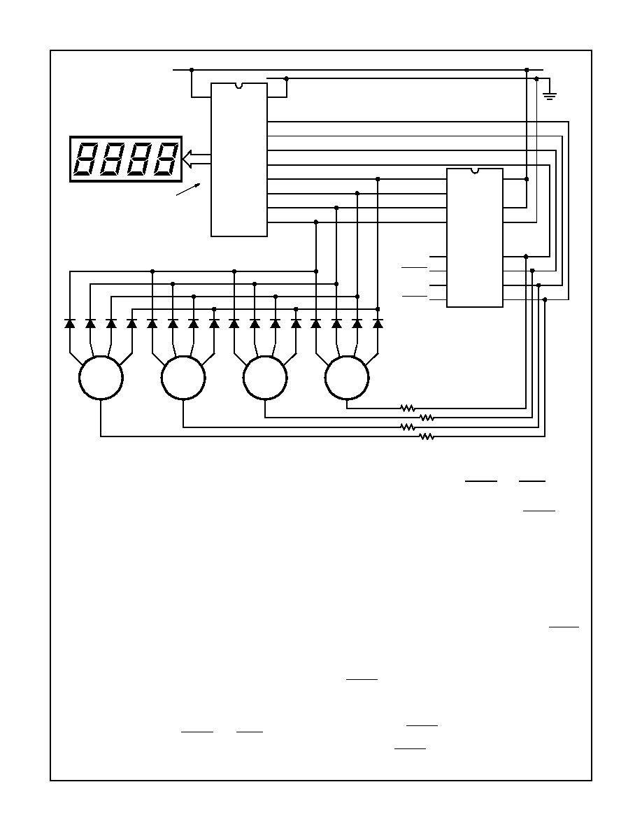
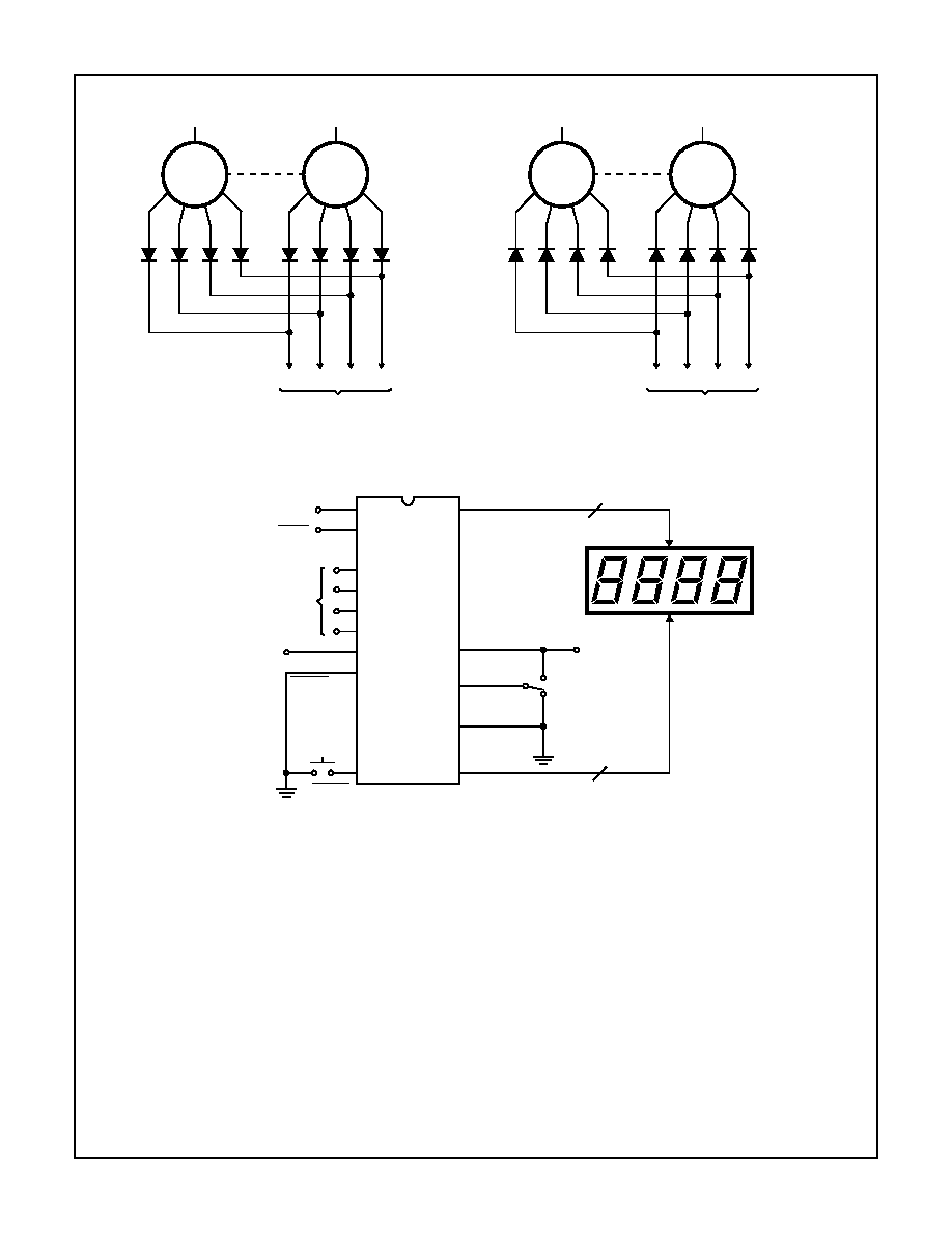
FIGURE 14. LCD DISPLAY INTERFACE (WITH THUMBWHEEL SWITCHES)
8
4
2
1
C
8
4
2
1
C
8
4
2
1
C
8
4
2
1
C
D4
D3
D2
D1
DB3
DB2
DB1
DB0
35
34
33
32
31
30
29
28
27
37 - 40
2 - 26
ICM7211
28 SEGMENTS
AND BACKPLANE
LCD DISPLAY
ICM7217
IJI
D1
D2
D3
D4
4
5
6
7
8s
4s
2s
1s
V
DD
DC
24
23
20
8
9
10
14
RESET
STORE
UP/DN
COUNT
28
27
26
25
V
DD
= 5V
V
DD
= 5V
10k
- 20k
ICM7217
12
When using the circuit as a programmable divider
(˜ by n
with equal outputs) a short time delay (about 1
µs) is needed
from the EQUAL output to the RESET input to establish a
pulse of adequate duration. (See Figure 16).
When the circuit is configured to reload the counter or regis-
ter with a new value from the BCD lines (upon reaching
EQUAL), loading time will be digit "on" time multiplied by
four. If this load time is longer than one period of the input
count, a count can be lost. Since the circuit will retain data in
the register, the register need only be updated when a new
value is to be entered. RESET will not clear the register.
Test Circuit
N.O.
V
DD
ICM7217
0.047
µF
RESET INPUT
10
V
SS
10k
5k
FIGURE 15. POWER ON RESET
V
DD
RESET
EQUAL
47pF
33K
FIGURE 16. EQUAL TO RESET DELAY
CARRY
ZERO
EQUAL
BCD I/O 8s
BCD I/O 4s
BCD I/O 2s
BCD I/O 1s
COUNT INPUT
STORE
UP/DOWN
LOAD REGISTER
LOAD COUNTER
SCAN
RESET
DISPLAY
28
27
26
25
24
23
22
21
20
19
18
17
16
15
ICM7217
ICM7217B
9999
1
2
3
4
5
6
7
8
9
10
11
12
13
14
a
b
c
d
f
g
e
a
b
c
d
f
g
e
a
b
c
d
f
g
e
a
b
c
d
f
g
e
g
b
e
f
d
a
c
COMMON ANODE DISPLAY
D1
D3
D2
D4
D1
D3
D2
D4
N.O.
V
DD
V
SS
CONTROL
V
DD
THUMBWHEEL SWITCHES
+5V
ICM7217

13
Applications
3-Level Inputs
ICM7217 has three inputs with 3-level logic states; High, Low
and Disconnected. These inputs are: LOAD REGISTER/OFF,
LOAD COUNTER/I/O OFF and DISPLAY CONT.
The circuits illustrated on Figure 11 can be used to drive
these inputs in different applications.
Fixed Decimal Point
In the common anode versions, a fixed decimal point may be
activated by connecting the DP segment lead from the appro-
priate digit (with separate digit displays) through a 39
series
resistor to Ground. With common cathode devices, the DP
segment lead should be connected through a 75
series
resistor to V
DD
.
To force the device to display leading zeroes after a fixed
decimal point, use a bipolar transistor and base resistor in a
configuration like that shown in Figure 12 with the resistor
connected to the digit output driving the DP for left hand DP
displays, and to the next least significant digit output for right
hand DP display.
Driving Larger Displays
For displays requiring more current than the ICM7217 can
provide, the circuits of Figure 13 can be used.
LCD Display Interface
The low-power operation of the ICM7217 makes an LCD
interface desirable. The Intersil ICM7211 4-digit, BCD-to-LCD
display driver easily interfaces to the ICM7217 as shown in
Figure 14. Total system power consumption is less than
5mW. System timing margins can be improved by using
capacitance to ground to slow down the BCD lines.
The 10k
- 20k resistors on the switch BCD lines serve to
isolate the switches during BCD output.
Unit Counter with BCD Output
The simplest application of the ICM7217 is a 4-digit unit
counter (Figure 18). All that is required is an ICM7217, a
power supply and a 4 digit display. Add a momentary switch
for reset, an SPDT center-off switch to blank the display or
view leading zeroes, and one more SPDT switch for up/
down control. Using an ICM7217A with a common-cathode
calculator-type display results in the least expensive digital
counter/display system available.
Inexpensive Frequency Counter/ Tachometer
This circuit uses the low power ICM7555 (CMOS 555) to
generate the gating, STORE and RESET signals as shown
in Figure 19. To provide the gating signal, the timer is con-
figured as an a stable multivibrator, using R
A
, R
B
and C to
provide an output that is positive for approximately one sec-
ond and negative for approximately 300
µs - 500µs. The pos-
itive waveform time is given by t
WP
= 0.693 (R
A
+ R
B
)C
while the negative waveform is given by two = 0.693 R
B
C.
The system is calibrated by using a 5M
potentiometer for
R
A
as a "coarse" control and a 1k
potentiometer for R
B
as
a "fine" control. CD40106Bs are used as a monostable
multivibrator and reset time delay.
Tape Recorder Position Indicator/controller
The circuit in Figure 20 shows an application which uses the
up/down counting feature of the ICM7217 to keep track of
tape position. This circuit is representative of the many
applications of up/down counting in monitoring dimensional
position.
In the tape recorder application, the LOAD REGISTER,
EQUAL and ZERO outputs are used to control the recorder.
To make the recorder stop at a particular point on the tape,
the register can be set with the stop point and the EQUAL
output used to stop the recorder either on fast forward, play
or rewind.
To make the recorder stop before the tape comes free of the
reel on rewind, a leader should be used. Resetting the
counter at the starting point of the tape, a few feet from the
end of the leader, allows the ZERO output to be used to stop
the recorder on rewind, leaving the leader on the reel.
The 1M
resistor and 0.0047µF capacitor on the COUNT
INPUT provide a time constant of about 5ms to debounce
the reel switch. The Schmitt trigger on the COUNT INPUT of
the ICM7217 squares up the signal before applying it to the
counter. This technique may be used to debounce
switch-closure inputs in other applications.
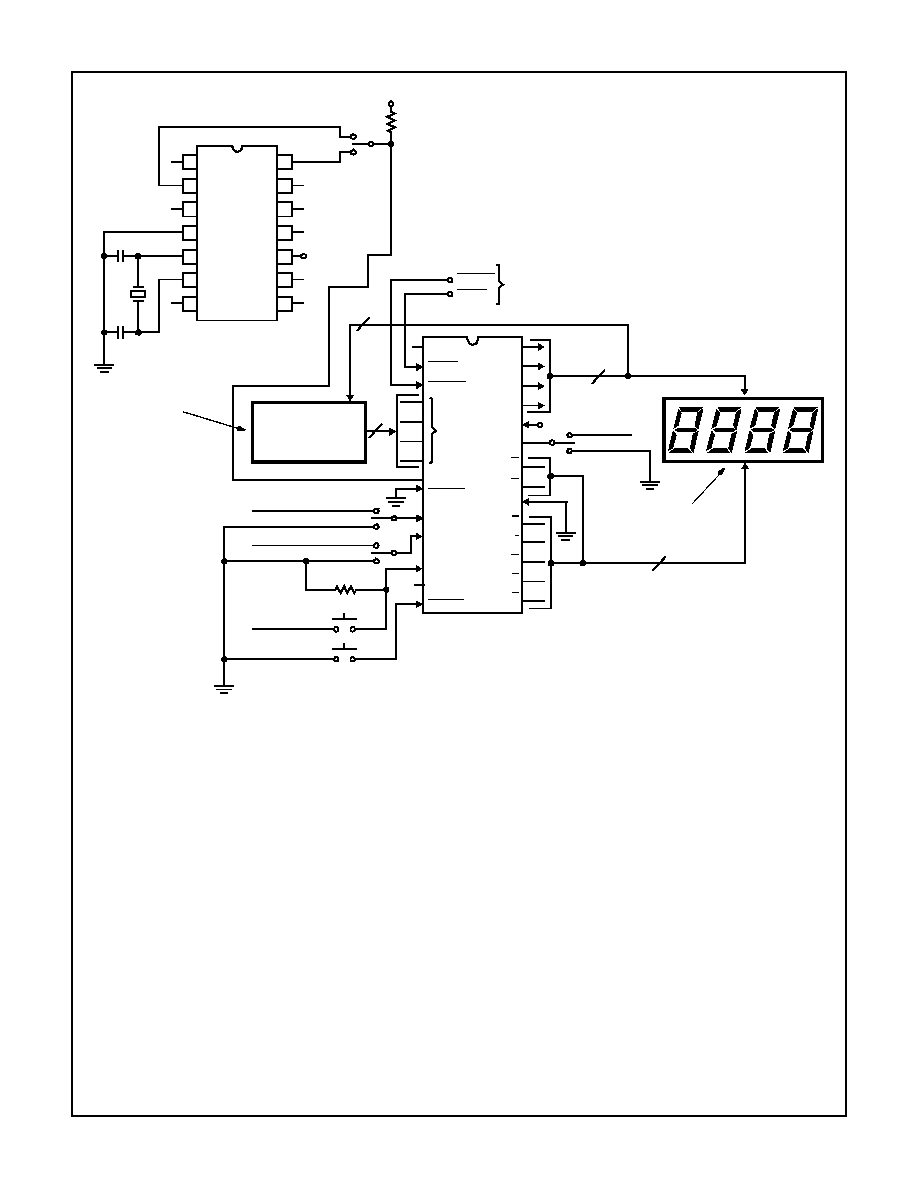
Precision Elapsed Time/Countdown Timer
The circuit in Figure 21 uses an ICM7213 precision one
minute/one second timebase generator using a 4.1943MHz
crystal for generating pulses counted by an ICM7217B. The
thumbwheel switches allow a starting time to be entered into
the counter for a preset-countdown type timer, and allow the
register to be set for compare functions. For instance, to
make a 24-hour clock with BCD output the register can be
preset with 2400 and the EQUAL output used to reset the
counter. Note the 10K resistor connected between the LOAD
COUNTER terminal and Ground. This resistor pulls the
LOAD COUNTER input low when not loading, thereby
inhibiting the BCD output drivers. This resistor should be
eliminated and SW4 replaced with an SPDT center-off
switch if the BCD outputs are to be used.
This technique may be used on any 3-level input. The 100k
pullup resistor on the count input is used to ensure proper
logic voltage swing from the ICM7213. For a less expensive
(and less accurate) timebase, an ICM7555 timer may be
used in a configuration like that shown in Figure 19 to
generate a 1Hz reference.
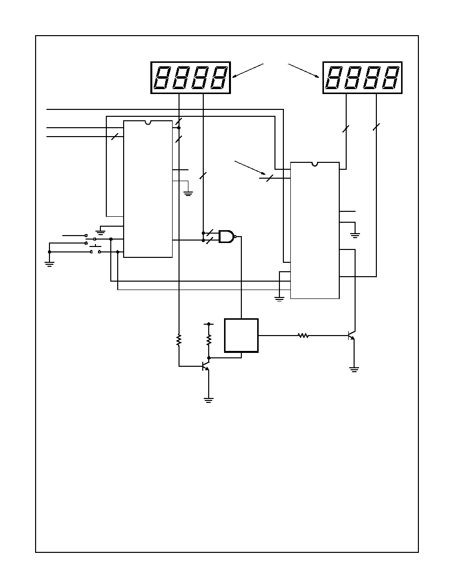
8-Digit Up/Down Counter
This circuit (Figure 22) shows how to cascade counters and
retain correct leading zero blanking. The NAND gate detects
whether a digit is active since one of the two segments a or b
is active on any unblanked number. The flip flop is clocked
by the least significant digit of the high order counter, and if
this digit is not blanked, the Q output of the flip flop goes high
and turns on the NPN transistor, thereby inhibiting leading
zero blanking on the low order counter.
ICM7217
14
It is possible to use separate thumbwheel switches for
presetting, but since the devices load data with the oscillator
free-running, the multiplexing of the two devices is difficult to
synchronize.
Precision Frequency Counter/Tachometer
The circuit shown in Figure 23 is a simple implementation of
a four digit frequency counter, using an ICM7207A to pro-
vide the one second gating window and the STORE and
RESET signals. In this configuration, the display reads hertz
directly. With Pin 11 of the ICM7027A connected to V
DD
, the
gating time will be 0.1s; this will display tens of hertz at the
least significant digit. For shorter gating times, an ICM7207
may be used (with a 6.5536MHz crystal), giving a 0.01s gat-
ing with Pin 11 connected to V
DD
, and a 0.1s gating with Pin
11 open.
To implement a four digit tachometer, the ICM7207A with
one second gating should be used. To get the display to
read directly in RPM, the rotational frequency of the object to
be measured must be multiplied by 60. This can be done
electronically using a phase-locked loop, or mechanically by
using a disc rotating with the object with the appropriate
number of holes drilled around its edge to interrupt the light
from an LED to a photo-dector. For faster updating, use 0.1s
gating, and multiply the rotational frequency by 600.
Auto-Tare System
This circuit uses the count-up and count-down functions of
the ICM7217, controlled via the EQUAL and ZERO outputs,
to count in SYNC with an ICL7109A and ICL7109D Con-
verter as shown in Figure 24. By RESETing the ICM7217 on
a "tare" value conversion, and STORE-ing the result of a true
value conversion, an automatic fare subtraction occurs in the
result.
The ICM7217 stays in step with the ICL7109 by counting up
and down between 0 and 4095, for 8192 total counts, the
same number as the ICL7109 cycle. See applications note
No. A047 for more details.
TABLE 2. CONTROL INPUT DEFINITIONS ICM7217
INPUT
TERMINAL
VOLTAGE
FUNCTION
STORE
9
V
DD
(or floating)
V
SS
Output Latches Not Updated
Output Latches Updated
UP/DOWN
10
V
DD
(or floating)
V
SS
Counter Counts Up
Counter Counts Down
RESET
14
V
DD
(or floating)
V
SS
Normal Operation
Counter Reset
LOAD COUNTER/
I/O OFF
12
Unconnected
V
DD
V
SS
Normal Operation
Counter Loaded with BCD data
BCD Port Forced to Hi-Z Condition
LOAD REGlSTER/
OFF
11
Unconnected
V
DD
V
SS
Normal Operation
Register Loaded with BCD Data
Display Drivers Disabled; BCD Port
Forced to Hi-Z Condition, mpx Counter
Reset to D4; mpx Oscillator Inhibited
DISPLAY CONTrol
23 Common Anode
20 Common Cathode
Unconnected
V
DD
V
SS
Normal Operation
Segment Drivers Disabled
Leading Zero Blanking Inhibited
ICM7217
15
FIGURE 17. THUMBWHEEL SWITCH/DIODE CONNECTIONS
FIGURE 18. UNIT COUNTER
8
4 2
1
C
8
4
2
1
C
TO D4 STROBE
TO D1 STROBE
8
4
2
1
TO BCD INPUTS OF ICM7217, ICM7217B
8
4 2
1
C
8
4 2
1
C
TO D4 STROBE
TO D1 STROBE
8
4
2
1
TO BCD INPUTS OF ICM7217A, ICM7217C
IN914 OR
EQUIVALENT
21 - 23
25 - 28
24
20
19
15 - 18
1
2
4
5
6
7
8
9
14
CARRY
ZERO
BCD I/O
COUNT INPUT
STORE
RESET
V
DD
DISPLAY
ICM7217A
4-DIGIT
CONTROL
BLANK
NORMAL
INHIBIT LZB
COMMON CATHODE
LED DISPLAY
7 SEGMENTS
ICM7217
16
FIGURE 19A.
FIGURE 19B.
FIGURE 19. INEXPENSIVE FREQUENCY COUNTER
FIGURE 20. TAPE RECORDER POSITION INDICATOR
ICM7217
4
5
6
7
V
DD
24
8
9
14
RESET
STORE
COUNT
V
SS
20
LED DISPLAY
8
2
1
V
SS
CV
TH
TR
DIS
OUT
V
DD
RS
R
A
R
B
0.47
µF
C
1K
5M
3
0.047
µF
3K
10K
COUNT INPUT
GND
GATE
INVERTERS: CD40106B
NANDS: CD4011B
300
µs
1s
50
µs
GATE
STORE
RESET
g
7 SEGMENTS
b
e
f
d
a
V
DD
4 DIGITS
BLANK
NORMAL
INHIBIT LZB
COMMON CATHODE
LED DISPLAY
D4
D3
D2
D1
CARRY
ZERO
BCD I/O
COUNT IN
STORE
RESET
c
EQUAL
UP/DOWN
LOAD REG
LOAD CTR
SCAN
ZERO
EQ
STOP
9999
4 DIGIT
RESET
N.O.
N.O.
V
DD
V
DD
FORWARD
REWIND
0.0047
µF
REEL SWITCH
CLOSED ONCE/REV
V
DD
1M
THUMBWHEEL SWITCHES
LOGIC TO GENERATE
RECORDER CONTROL
SIGNALS
SET PT
1
28
V
DD
ICM7217
17
FIGURE 21. PRECISION TIMER
1
2
3
4
5
6
7
14
13
12
11
10
9
8
RUN MIN/SEC
STOP
RUN HRS/MIN
V
DD
(4V MAX)
SW1
g
4
b
e
f
d
a
V
DD
7
BLANK
SW6
INHIBIT
COMMON ANODE
LED DISPLAY
D4
D3
D2
D1
CARRY
ZERO
BCD
COUNT IN
STORE
RESET
c
EQUAL
UP/DOWN
LOAD REG
LOAD CTR
SCAN
LZB
V
DD
DIGITS
V
DD
DIS. CONT.
I/O
V
SS
SEGMENTS
5959
4
4
V
DD
V
DD
V
DD
RESET
PRESET
DISPLAY OFF
LOAD SET PT.
10K
SW3
SW2
COUNTDOWN
ELAPSED
SW4
SW5
EQUAL
ZERO
TO LOGIC GENERATING
SIGNALS FOR CONTROL OF
EXTERNAL EQUIPMENT
100K
V
DD
THUMBWHEEL SWITCHES
ICM7217
ICM7213
30pF
30pF
4.1943MHz
CRYSTAL
R
S
< 75
ICM7217
18
FIGURE 22. 8-DIGIT UP/DOWN COUNTER
1
4 - 7
8
9
10
14
25 - 28
24
20
23
15 - 19
21, 22
ICM7217
LOW ORDER
V+
1
4 - 7
8
9
10
14
25 - 28
24
20
15 - 19
21, 22
ICM7217
HIGH ORDER
V+
50k
3k
V+
D
Q
CL
CD4013
1
/
2
V+
CARRY OUT
BCD OUTPUTS
COUNT INPUT
UP/DOWN
4 DIGITS
RESET
4
D1
N.O.
HIGH ORDER DIGITS
50k
NPN
TRANSISTOR
BCD OUTPUTS
HIGH ORDER DIGITS
4
CARRY/BORROW
7 SEGMENTS
1B
1A
CD4011
1
/
4
4 DIGITS
7 SEGMENTS
COMMON-ANODE
LED DISPLAY
ICM7217
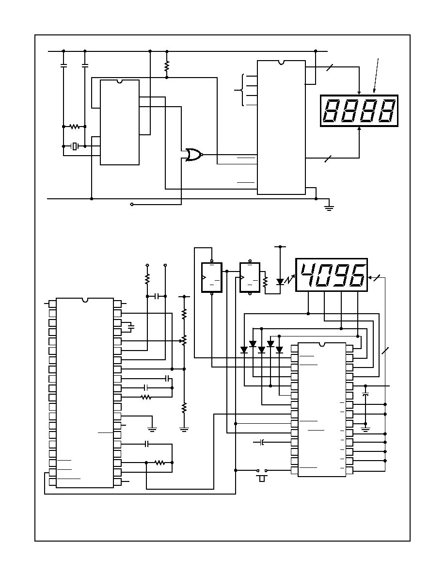
19
FIGURE 23. PRECISION FREQUENCY COUNTER (MHz MAXIMUM)
FIGURE 24. AUTO-TARE SYSTEM FOR A/D CONVERTER
4
8
9
14
25 - 28
24
20
15 - 19
21, 22
ICM7217
4 DIGITS
7 SEGMENTS
COMMON ANODE
LED DISPLAY
5
6
7
BCD
COUNT
STORE
RESET
OUT
ICM7207A
4
5
6
2
13
14
10
CD4011
1
/
4
INPUT
10k
22pF
22pF
CRYSTAL
f
= 5.24288MHz
R
S
= 75
V+ = 5V
10k
13
1
2
3
4
5
6
7
8
9
10
11
12
14
15
16
17
18
19
20
28
40
39
38
37
36
35
34
33
32
31
30
29
27
26
25
24
23
22
21
ICM7109
V
DD
REF IN -
REF CAP -
REF CAP +
REF IN +
IN HI
IN LO
COMMON
INT
AZ
BUF
REF OUT
V
SS
SEND
RUN/HOLD
BUF OSC OUT
OSC SEL
OSC OUT
OSC IN
MODE
GND
STATUS
POL
OR
B12
B11
B10
B9
B8
B7
B6
B5
B4
B3
B2
B1
TEST
LBEN
HBEN
CE/LOAD
CARRY/
ZERO
EQUAL
BCD 8
BCD 4
BCD 2
BCD 1
COUNT
STORE
UP/DOWN
LOAD REG.
LOAD CTR.
SCAN
RESET
D0
D2
D3
V
DD
DISP.
B
E
F
D
A
C
D1
G
V
SS
28
27
26
25
24
23
22
21
20
19
18
17
16
15
1
2
3
4
5
6
7
8
9
10
11
12
13
14
BORROW
CONT.
ICM7217
7
7
TARE
10
µF
+5V
+5V
5 x 1N4148
MINUS SIGN
LED
270
+5V
4 DIGIT COMMON ANODE
LED DISPLAY
Q
D
Q
D
Q
Q
R
R
S
S
47
µF
100K
10K
100K
+5V
0.1
µF
+
100K
100pF
+5V
47K
0.22
µF
0.1
µF
1
µF
+5V
-
+5V
400mV
FULL SCALE
INPUT