 | –≠–ª–µ–∫—Ç—Ä–æ–Ω–Ω—ã–π –∫–æ–º–ø–æ–Ω–µ–Ω—Ç: ICM7218DI | –°–∫–∞—á–∞—Ç—å:  PDF PDF  ZIP ZIP |
1
TM
File Number
3159.1
CAUTION: These devices are sensitive to electrostatic discharge; follow proper IC Handling Procedures.
1-888-INTERSIL or 321-724-7143
|
Intersil and Design is a trademark of Intersil Americas Inc.
Copyright © Intersil Americas Inc. 2001, All Rights Reserved
ICM7218
8-Digit LED Microprocessor-Compatible
Multiplexed Display Decoder Driver
The ICM7218 series of universal LED driver systems
provide, in a single package, all the circuitry necessary to
interface most common microprocessors or digital systems
to an LED display. Included on chip are an 8-byte static
display memory, two types of 7-segment decoders, multiplex
scan circuitry, and high current digit and segment drivers for
either common-cathode or common-anode displays.
The lCM7218A and 1CM7218B feature two control lines
(WRITE and MODE) which write either 4 bits of control
information (DATA COMING, SHUTDOWN, DECODE, and
HEXA/CODE B) or 8 bits of display input data. Display data
is automatically sequenced into the 8-byte internal memory
on successive positive going WRITE pulses. Data may be
displayed either directly or decoded in Hexadecimal or Code
B formats.
The ICM7218C and lCM7218D feature two control lines
(WRITE and HEXA/CODE B/SHUTDOWN), 4 separate
display data input lines, and 3 digit address lines. Display
data is written into the internal memory by setting up a digit
address and strobing the WRITE line low. Only Hexadecimal
and Code B formats are available for display outputs.
Features
∑ Microprocessor Compatible
∑ Total Circuit Integration On Chip Includes:
- Digit and Segment Drivers
- All Multiplex Scan Circuitry
- 8-Byte Static Display Memory
- 7-Segment Hexadecimal and Code B Decoders
∑ Output Drive Suitable for LED Displays Directly
∑ Common Anode and Common Cathode Versions
∑ Single 5V Supply Required
∑ Data Retention to 2V Supply
∑ Shutdown Feature - Turns Off Display and Puts Chip Into
Low Power Dissipation Mode
∑ Sequential and Random Access Versions
∑ Decimal Point Drive On Each Digit
Related Literature
∑ Technical Brief TB363 "Guidelines for Handling and
Processing Moisture Sensitive Surface Mount Devices
(SMDs)"
Ordering Information
PART NUMBER
TEMP. RANGE (
o
C)
PACKAGE
PKG. NO.
DISPLAY TYPE
ICM7218AIJI
-40 to 85
28 Ld CERDIP
F28.6
Common Anode
ICM7218BIJI
-40 to 85
28 Ld CERDIP
F28.6
Common Cathode
ICM7218CIJI
-40 to 85
28 Ld CERDIP
F28.6
Common Anode
ICM7218DIJI
-40 to 85
28 Ld CERDIP
F28.6
Common Cathode
Data Sheet
March 2001
2
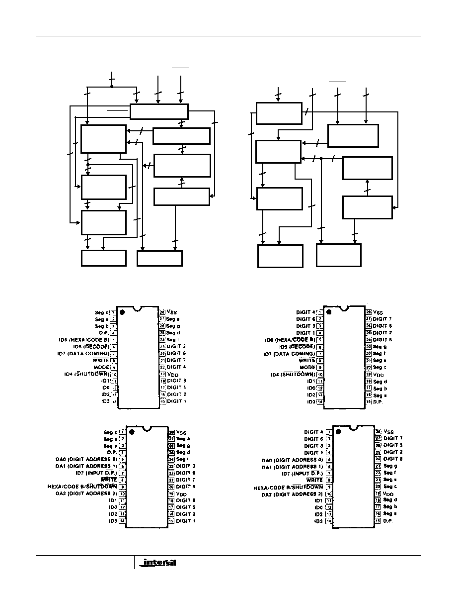
MULTIPLEX
OSCILLATOR
INTERDIGIT
BLANKING
8-DIGIT
DRIVERS
8-SEGMENT
DRIVERS
DECIMAL
POINT
7
7
1
3
DECODE/
NO-DECODE
HEXADECIMAL/
CODE B
DECODER
7
1
8
8
8
8
8
1
1
7
4
7
1
1
1
1
1
4
8
4
8
8
1
1
8
8
1
1
1
5
5
3
1
HEXADECIMAL/
CODE B
DECODER
MULTIPLEX
OSCILLATOR
8-DIGIT
DRIVERS
8-SEGMENT
DRIVERS
DECIMAL
POINT
INTERDIGIT
BLANKING
READ
ADRESS, DIGIT
MULTIPLEXER
READ
ADRESS
MULTIPLEXER
WRITE
ADDRESS
DECODER
WRITE ADDRESS
COUNTER
CONTROL
LOGIC
8-BYTE
STATIC
RAM
8-BYTE
STATIC
RAM
THREE LEVEL
INPUT LOGIC
SHUTDOWN
DECODE
HEXA/CODE B
SHUTDOWN
ID0-ID7
INPUT
DATA
ID4-ID7
CONTROL
INPUTS
MODE
WRITE
HEXADECIMAL/
CODE B/
SHUTDOWN
WRITE
ID0-ID3
INPUT
DATA
ID7
DA0-DA2
DIGIT
ADDRESS
ICM7218C COMMON ANODE
ICM7218D COMMON CATHODE
ICM7218A COMMON ANODE
ICM7218B COMMON CATHODE
FIGURE 1. FUNCTIONAL DIAGRAMS
Pinouts
ICM7218A TOP VIEW
ICM7218B TOP VIEW
ICM7218C TOP VIEW
ICM7218D TOP VIEW
FIGURE 2. PIN CONFIGURATIONS
ICM7218
3
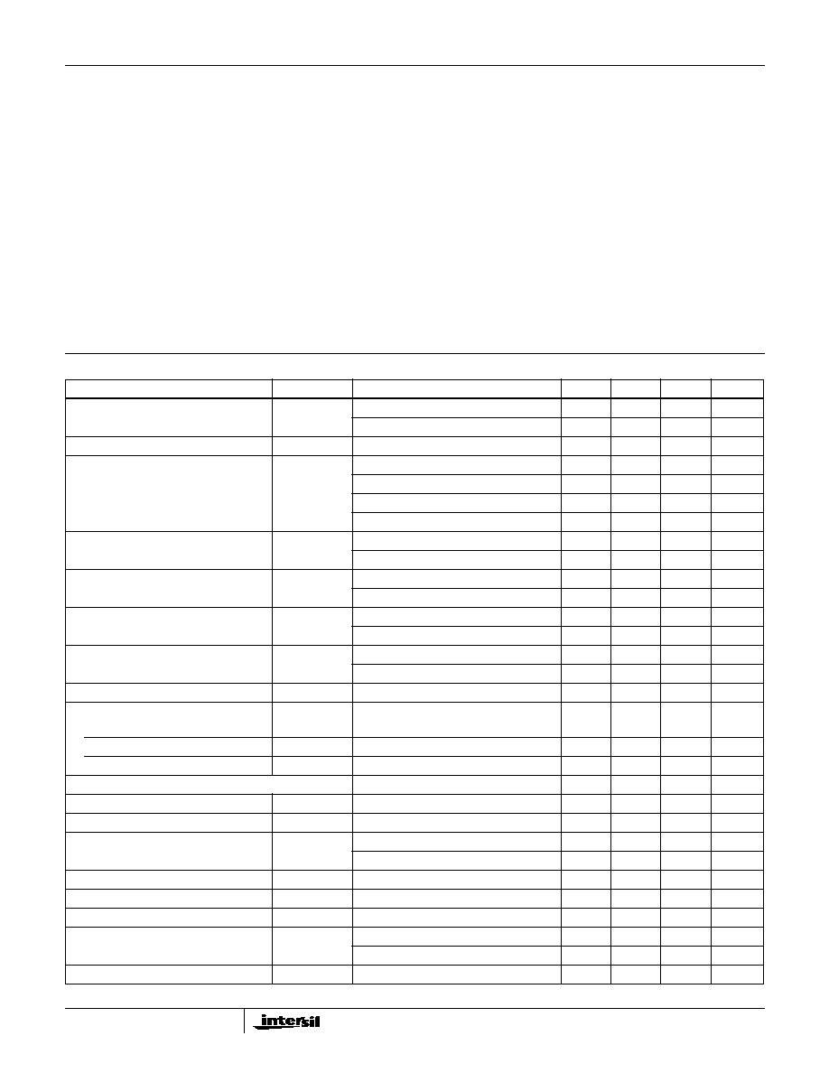
Absolute Maximum Ratings
Thermal Information
Supply Voltage (V
DD
to V
SS
). . . . . . . . . . . . . . . . . . . . . . . . . . . . 6V
Digit Output Current . . . . . . . . . . . . . . . . . . . . . . . . . . . . . . . . 300mA
Segment Output Current . . . . . . . . . . . . . . . . . . . . . . . . . . . . . 50mA
Input Voltage (Any Terminal)(Note 1). . . . V
SS
-0.3V to V
DD
+ 0.3V
Operating Conditions
Temperature Range . . . . . . . . . . . . . . . . . . . . . . . . . . -40
o
C to 85
o
C
Thermal Resistance (Typical, Note 2)
JA
(
o
C/W)
JC
(
o
C/W)
CERDIP Package . . . . . . . . . . . . . . . . .
55
14
Maximum Storage Temperature Range . . . . . . . . . . -65
o
C to 150
o
C
Maximum Lead Temperature (Soldering 10s) . . . . . . . . . . . . 300
o
C
CAUTION: Stresses above those listed in "Absolute Maximum Ratings" may cause permanent damage to the device. This is a stress only rating and operation of the
device at these or any other conditions above those indicated in the operational sections of this specification is not implied.
NOTE:
1. Due to the SCR structure inherent in the CM0S process used to fabricate these devices, connecting any terminal to a voltage greater than V
DD
or less than V
SS
may cause destructive device latchup. For this reason it is recommended that no inputs from sources operating on a different
power supply be applied to the device before its own supply is established, and when using multiple supply systems the supply to the ICM7218
should be turned on first.
2.
JA
is measured with the component mounted on a low effective thermal conductivity test board in free air. See Tech Brief TB379 for details.
Electrical Specifications
V
DD
= 5V, V
SS
= 0V, T
A
= 25
o
C, Display Diode Drop = 1.7V
PARAMETER
SYMBOL
TEST CONDITIONS
MIN
TYP
MAX
UNITS
Supply Voltage Range
V
SUPPLY
Operating
4
-
6
V
Power Down Mode
2
-
6
V
Quiescent Supply Current
I
Q
Shutdown (Note 3)
6
10
300
µ
A
Operating Supply Current - Outputs Open
Circuit
I
DD
Common Anode SEGS On (Note 6)
-
-
2.5
mA
Common Anode SEGS Off (Note 6)
-
-
500
µ
A
Common Cathode SEGS On (Note 6)
-
-
700
µ
A
Common Cathode SEGS Off (Note 6)
-
-
500
µ
A
Digit Drive Current
I
DIG
Common Anode V
OUT
= V
DD
-2.0V
140
200
-
mA
Common Cathode V
OUT
= V
SS
+1.0V
50
100
-
mA
Digit Leakage Current - Shutdown Mode
I
DLK
Common Anode V
OUT
= 2V
-
-
100
µ
A
Common Cathode V
OUT
= 5V
-
-
100
µ
A
Peak Segment Drive Current
I
SEG
Common Anode V
OUT
= V
SS
+1.0V
20
40
-
mA
Common Anode V
OUT
= V
DD
-2.0V
-10
-20
-
mA
Segment Leakage Current - Shutdown
Mode
I
SLK
Common Anode V
OUT
= V
DD
-
-
100
µ
A
Common Cathode V
OUT
= V
SS
-
-
100
µ
A
Display Scan Rate
f
MUX
Per Digit
-
250
-
Hz
Three Level Input (Pin 9 ICM7218C/D)
Logical "1" Input Voltage
V
IH
Hexadecimal
4.5
-
-
V
Floating Input
V
IF
Code B
2.0
-
3.0
V
Logical "0" Input Voltage
V
IL
Shutdown
-
-
0.4
V
Three Level Input Impedance
Z
IN
Note 3
-
100
-
k
Logical "1" Input Voltage
V
IH
3.5
-
-
V
Logical "0" Input Voltage
V
IL
-
-
0.8
V
Wrtie Pulse Width (Low)
t
WL
7218A, 7218B
550
400
-
ns
7218C, 7218D
400
250
-
ns
Mode Hold Time
t
MH
7218A, 7218B
150
-
-
ns
Mode Setup Time
t
MS
7218A, 7218B
500
-
-
ns
Data Setup Time
t
DS
500
-
-
ns
Data Hold Time
t
DH
7218A, 7218B
50
-
-
ns
7218C, 7218D
125
-
-
ns
Digital Address Setup Time
t
AS
7218C, 7218D
500
-
-
ns
ICM7218
4
Digital Address Hold Time
t
AH
7218C, 7218D
0
-
-
ns
Data Input Impedance
Z
IN
5-10pF Gate Capacitance
-
10
10
-
NOTES:
3. In the ICM7218C and D (random access versions) the HEXA/CODE B/SHUTDOWN input (Pin 9) has internal biasing resistors to hold it at V
DD
/2
when Pin 9 is open-circuited. These resistors consume power and result in a quiescent supply current (I
Q
) of typically 50
µ
. The ICM7218A,
and B devices do not have these biasing resistors and thus are not subject to this condition.
Electrical Specifications
V
DD
= 5V, V
SS
= 0V, T
A
= 25
o
C, Display Diode Drop = 1.7V (Continued)
PARAMETER
SYMBOL
TEST CONDITIONS
MIN
TYP
MAX
UNITS
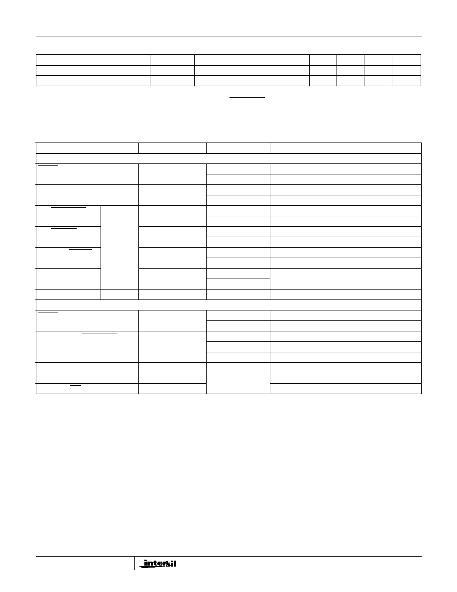
Pin Descriptions
INPUT
TERMINAL
LOGIC LEVEL
FUNCTION
ICM7218A AND ICM7218B
WRITE
8
High
Input Not Loaded
Low
Input Loaded
MODE
9
High
Load Control Bits on Write Pulse
Low
Load Input Data on Write Pulse
ID4 (SHUTDOWN)
MODE High
10
High
Normal Operation
Low
Shutdown (Oscillator, Decoder and Display Disabled)
ID5 (DECODE)
6
High
No Decode
Low
Decode
ID6 (HEXA/CODE B)
5
High
Hexadecimal Decoding
Low
Code B Decoding
ID7 (DATA COMING)
7
High
Data Coming
No Data Coming
Low
ID0-ID7
MODE Low
11, 12, 13, 14, 5, 6, 10, 7
Display Data Inputs (Notes 4, 5)
ICM7218C AND ICM7218D
WRITE
8
High
Input Not Loaded into Memory
Low
Input Loaded into Memory
HEXA/CODE B/ SHUTDOWN
9 (Note 3)
High
Hexadecimal Decoding
Floating
Code B Decoding
Low
Shutdown (Oscillator, Decoder and Display Disabled)
DA0 - DA2
10, 6, 5
Digit Address Inputs
ID0 - ID3
14, 13, 11, 12
Display Data Inputs
ID7 (INPUT D.P.)
7
Decimal Point Input
NOTES:
4. ID0-ID3 = Don't Care when writing control data.
ID4-ID6 = Don't Care when writing Hex/Code B data.
ID7 = Decimal Point data.
(The display blanks on ICM7218A/B versions when writing in data).
5. In the No Decode format, "Ones" represents "on" segments for all inputs except for the Decimal Point, where "Zero" represents an "on" segment
(i.e., segments are positive true, decimal point is negative true).
6. Common Anode segment drivers and Common Cathode Digit Drivers have 20k
pullup resistors.
}
Control Word
ICM7218
5
Detailed Description
DECODE Operation
For the lCM7218A/B products, there are 3 input data formats
possible; either direct segment and decimal point information (8
bits per digit) or two Binary formats plus decimal point
information (Hexadecimal/Code B formats with 5 bits per digit).
The 7-segment decoder on chip is disabled when direct
segment information is to be written. In this format, the
inputs directly control the outputs as follows:
Here, "Ones" represent "on" segments for all inputs except
the Decimal Point. For the Decimal Point "zero" represents
an "on" segment.
HEXAdecimal/CODE B Decoding
For all products, a choice of either HEXA or Code B decoding
may be made. HEXA decoding provides 7-segment numeric
plus six alpha characters while Code B provides a negative
sign (-), a blank (for leading zero blanking), certain useful
alpha characters and all numeric formats.
The four bit binary code is set up on inputs lD3-lD0, and
decimal point data is set up on ID7.
SHUTDOWN
SHUTDOWN performs several functions: it puts the device
into a very low dissipation mode (typically 10
µ
A at V
DD
= 5V),
turns off both the digit and segment drivers, and stops the
multiplex scan oscillator (this is the only way the scan
oscillator can be disabled). However, it is still possible to input
data to the memory during shutdown - only the display output
sections of the device are disabled in this mode.
Powerdown
In the Shutdown Mode, the supply voltage may be reduced to
2V without data in memory being lost. However, data should
not be written into memory if the supply voltage is less than 4V.
Output Drive
The common anode output drive is approximately 200mA per
digit at a 12% duty cycle. With segment peak drive current of
40mA typically, this results in 5mA average drive. The common
cathode drive capability is approximately one-half that of the
common anode drive. If high impedance LED displays are
used, the drive current will be correspondingly less.
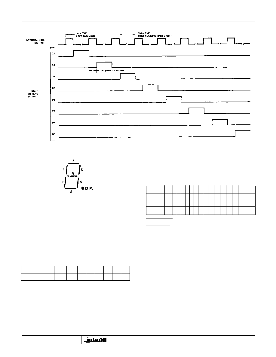
FIGURE 3. MULTIPLEX TIMING (COMMON CATHODE VERSION)
Input Data:
ID7
lD6
ID5 lD4 lD3 lD2 lD1 ID0
Output Segments:
D.P.
a
b
c
e
g
f
d
FIGURE 4. SEGMENT ASSIGNMENTS
DECIMAL 0 1 2 3 4 5 6 7 8 9 10 11 12 13 14
15
HEXA
CODE
0 1 2 3 4 5 6 7 8 9 A
B
C
D
E
F
CODE B
0 1 2 3 4 5 6 7 8 9
-
E
H
L
P
(BLANK)
ICM7218