
9-17
August 1997
ICM7228
8-Digit, Microprocessor-
Compatible, LED Display Decoder Driver
Features
∑ Improved 2nd Source to Maxim ICM7218
∑ Fast Write Access Time of 200ns
∑ Multiple Microprocessor Compatible Versions
∑ Hexadecimal, Code B and No Decode Modes
∑ Individual Segment Control with "No Decode" Feature
∑ Digit and Segment Drivers On-Chip
∑ Non-Overlapping Digits Drive
∑ Common Anode and Common Cathode LED Versions
∑ Low Power CMOS Architecture
∑ Single 5V Supply
Applications
∑ Instrumentation
∑ Test Equipment
∑ Hand Held Instruments
∑ Bargraph Displays
∑ Numeric and Non-Numeric Panel Displays
∑ High and Low Temperature Environments where LCD
Display Integrity is Compromised
Description
The Intersil ICM7228 display driver interfaces microproces-
sors to an 8-digit, 7-segment, numeric LED display. Included
on chip are two types of 7-segment decoder, multiplex scan
circuitry, LED display segment drivers, LED display digit
drivers and an 8-byte static memory as display RAM.
Data can be written to the ICM7228A and ICM7228B's display
RAM in sequential 8-digit update or in single-digit update for-
mat. Data is written to the ICM7228C and ICM7228D display
RAM in parallel random access format. The ICM7228A and
ICM7228C drive common anode displays. The ICM7228B and
ICM7228D drive common cathode displays. All versions can
display the RAM data as either Hexadecimal or Code B format.
The ICM7228A and ICM7228B incorporate a No Decode mode
allowing each bit of each digit's RAM word to drive individual
display segments resulting in independent control of all display
segments. As a result, bargraph and other irregular display
segments and formats can be driven directly by this chip.
The Intersil ICM7228 is an alternative to both the Maxim
ICM7218 and the Intersil ICM7218 display drivers. Notice that
the ICM7228A/B has an additional single digit access mode.
This could make the Intersil ICM7218A/B software incompatible
with ICM7228A/B operation.
Ordering Information
PART NUMBER
DATA ENTRY PROTOCOL
DISPLAY TYPE
TEMP. RANGE (
o
C)
PACKAGE
PKG. NO.
ICM7228AIPI
Sequential
Common Anode
-40 to 85
28 Ld PDIP
E28.6
ICM7228BIPI
Sequential
Common Cathode
-40 to 85
28 Ld PDIP
E28.6
ICM7228CIPI
Random
Common Anode
-40 to 85
28 Ld PDIP
E28.6
ICM7228DIPI
Random
Common Cathode
-40 to 85
28 Ld PDIP
E28.6
ICM7228AIJI
Sequential
Common Anode
-40 to 85
28 Ld CERDIP
F28.6
ICM7228BIJI
Sequential
Common Cathode
-40 to 85
28 Ld CERDIP
F28.6
ICM7228CIJI
Random
Common Anode
-40 to 85
28 Ld CERDIP
F28.6
ICM7228DIJI
Random
Common Cathode
-40 to 85
28 Ld CERDIP
F28.6
ICM7228AIBI
Sequential
Common Anode
-40 to 85
28 Ld SOIC
M28.3
ICM7228BIBI
Sequential
Common Cathode
-40 to 85
28 Ld SOlC
M28.3
ICM7228CIBI
Random
Common Anode
-40 to 85
28 Ld SOlC
M28.3
ICM7228DIBI
Random
Common Cathode
-40 to 85
28 Ld SOlC
M28.3
ICM7228AMJI883B
Sequential
Common Anode
-55 to 125
28 Ld CERDIP
F28.6
ICM7228BMJI883B
Sequential
Common Cathode
-55 to 125
28 Ld CERDIP
F28.6
ICM7228CMJI883B
Random
Common Anode
-55 to 125
28 Ld CERDIP
F28.6
ICM7228DMJI883B
Random
Common Cathode
-55 to 125
28 Ld CERDIP
F28.6
File Number
3160.1
CAUTION: These devices are sensitive to electrostatic discharge; follow proper IC Handling Procedures.
http://www.intersil.com or 407-727-9207
|
Copyright
©
Intersil Corporation 1999

9-18
Pinouts
ICM7228A
(CERDIP, PDIP, SOIC)
COMMON ANODE
TOP VIEW
ICM7228B
(CERDIP, PDIP, SOIC)
COMMON CATHODE
TOP VIEW
ICM7228C
(CERDIP, PDIP, SOIC)
COMMON ANODE
TOP VIEW
ICM7228D
(CERDIP, PDIP, SOIC)
COMMON CATHODE
TOP VIEW
SEG
c
SEG
e
SEG
b
DP
ID6 (HEXA/CODE B)
ID5 (DECODE)
ID7 (DATA COMING)
WRITE
MODE
ID4 (SHUTDOWN)
ID1
ID0
ID2
ID3
V
SS
SEG
g
SEG
d
SEG
f
DIGIT 3
DIGIT 7
V
DD
DIGIT 8
DIGIT 5
DIGIT 2
DIGIT 1
SEG
a
DIGIT 6
DIGIT 4
28
27
26
25
24
23
22
21
20
19
18
17
16
15
1
2
3
4
5
6
7
8
9
10
11
12
13
14
DIGIT 4
DIGIT 6
DIGIT 3
DIGIT 1
ID6 (HEXA/CODE B)
ID5 (DECODE)
ID7 (DATA COMING)
WRITE
MODE
ID4 (SHUTDOWN)
ID1
ID0
ID2
ID3
V
SS
DIGIT 5
DIGIT 2
DIGIT 8
SEG
g
SEG
e
V
DD
SEG
d
SEG
b
SEG
a
DP
DIGIT 7
SEG
f
SEG
c
28
27
26
25
24
23
22
21
20
19
18
17
16
15
1
2
3
4
5
6
7
8
9
10
11
12
13
14
SEG
c
SEG
e
SEG
b
DP
DA0 (DIGIT ADDRESS 0)
DA1 (DIGIT ADDRESS 1)
ID7 (INPUT DP)
WRITE
HEXA/CODE B/SHUTDOWN
DA2 (DIGIT ADDRESS 2)
ID1
ID0
ID2
ID3
V
SS
SEG
g
SEG
d
SEG
f
DIGIT 3
DIGIT 7
V
DD
DIGIT 8
DIGIT 5
DIGIT 2
DIGIT 1
SEG
a
DIGIT 6
DIGIT 4
28
27
26
25
24
23
22
21
20
19
18
17
16
15
1
2
3
4
5
6
7
8
9
10
11
12
13
14
DIGIT 4
DIGIT 6
DIGIT 3
DIGIT 1
DA0 (DIGIT ADDRESS 0)
DA1 (DIGIT ADDRESS 1)
ID7 (INPUT DP)
WRITE
HEXA/CODE B/SHUTDOWN
DA2 (DIGIT ADDRESS 2)
ID1
ID0
ID2
ID3
V
SS
DIGIT 5
DIGIT 2
DIGIT 8
SEG
g
SEG
e
V
DD
SEG
d
SEG
b
SEG
a
DP
DIGIT 7
SEG
f
SEG
c
28
27
26
25
24
23
22
21
20
19
18
17
16
15
1
2
3
4
5
6
7
8
9
10
11
12
13
14
ICM7228
9-19
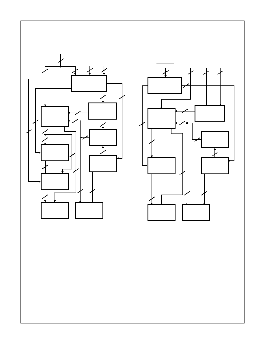
Functional Block Diagram
8 SEGMENT
DRIVERS
8 DIGIT
DRIVERS
DECODE
NO-DECODE
8-BYTE
STATIC
RAM
HEXADECIMAL/
CODE B
DECODER
MULTIPLEX
OSCILLATOR
WRITE ADDRESS
COUNTER
CONTROL
LOGIC
READ
ADDRESS, DIGIT
MULTIPLEXER
ICM7228A, ICM7228B
ID0 - ID7
INPUT
DATA
ID4 - ID7
CONTROL
INPUTS
MODE
WRITE
SHUTDOWN
HEXA/CODE B
DECODE
INTERDIGIT
BLANKING
DECIMAL
POINT
8
8
4
1
1
1
1
4
7
7
7
8
8
8
1
1
3
1
8
1
7
1
8 SEGMENT
DRIVERS
8 DIGIT
DRIVERS
8-BYTE
STATIC
RAM
HEXADECIMAL/
CODE B
DECODER
MULTIPLEX
OSCILLATOR
WRITE ADDRESS
COUNTER
THREE LEVEL
INPUT LOGIC
READ
ADDRESS
MULTIPLEXER
ICM7228C, ICM7228D
WRITE
SHUTDOWN
INTERDIGIT
BLANKING
DECIMAL
POINT
1
5
1
1
4
7
8
8
8
5
1
8
1
1
DA0 - DA2
3
DIGIT
ADDRESS
ID0 - ID3
ID7
DATA INPUT
HEXADECIMAL/
CODE B/
SHUTDOWN
ICM7228
9-20
Absolute Maximum Ratings
Thermal Information
Supply Voltage (V
DD
- V
SS
) . . . . . . . . . . . . . . . . . . . . . . . . . . . . . 6V
Digit Output Current . . . . . . . . . . . . . . . . . . . . . . . . . . . . . . . . 500mA
Segment Output Current . . . . . . . . . . . . . . . . . . . . . . . . . . . . 100mA
Input Voltage (Note 1) (Any Terminal). . .(V
SS
-0.3V)<V
IN
<(V
DD
+0.3V)
Operating Conditions
Operating Temperature Range
IPI, IJI, IBI Suffix . . . . . . . . . . . . . . . . . . . . . . . . . . . -40
o
C to 85
o
C
MJl Suffix . . . . . . . . . . . . . . . . . . . . . . . . . . . . . . . -55
o
C to 125
o
C
Thermal Resistance (Typical, Note 2)
JA
(
o
C/W)
JC
(
o
C/W)
CERDIP Package . . . . . . . . . . . . . . . .
55
12
PDIP Package . . . . . . . . . . . . . . . . . . .
60
N/A
SOIC Package . . . . . . . . . . . . . . . . . . .
75
N/A
Maximum Junction Temperature
IPI, IBI Suffix . . . . . . . . . . . . . . . . . . . . . . . . . . . . . . . . . . . . 150
o
C
MJI, IJI Suffix . . . . . . . . . . . . . . . . . . . . . . . . . . . . . . . . . . . . 175
o
C
Maximum Storage Temperature Range . . . . . . . . . .-65
o
C to 150
o
C
Maximum Lead Temperature (Soldering 10s) . . . . . . . . . . . . . 300
o
C
(SOIC - Lead Tips Only)
CAUTION: Stresses above those listed in "Absolute Maximum Ratings" may cause permanent damage to the device. This is a stress only rating and operation
of the device at these or any other conditions above those indicated in the operational sections of this specification is not implied.
NOTES:
1. Due to the SCR structure inherent in the CMOS process used to fabricate these devices, connecting any terminal to a voltage greater
than V
DD
or less then V
SS
may cause destructive device latchup. For this reason, it is recommended that no inputs row sources operating
on a different power supply be applied to the device before its own supply is established, and when using multiple supply systems the
supply to the ICM7228 should be turned on first.
2.
JA
is measured with the component mounted on an evaluation PC board in free air.
Electrical Specifications
V
DD
= +5.0V
±
10%, V
SS
= 0V, Unless Otherwise Specified
INDUSTRIAL TEMPERATURE RANGE, IPI, IJI, LBI DEVICES
PARAMETER
TEST CONDITIONS
T
A
= 25
o
C
-40
o
C TO 85
o
C
UNITS
MIN
TYP
MAX
MIN
TYP
MAX
Supply Voltage Range, V
SUPPLY
Operating
4
-
6
4
-
6
V
Power Down Mode
2
-
-
2
-
-
Quiescent Supply Current, I
Q
Shutdown, ICM7228A, IMC7228B
-
1
100
-
1
100
µ
A
Shutdown, 7228C, 7228D
-
2.5
100
-
2.5
100
Operating Supply Current, I
DD
Common Anode, ICM7228A/C
Segments = ON; Outputs = OPEN
-
200
450
-
200
450
µ
A
Common Anode, ICM7228A/C
Segments = OFF; Outputs = OPEN
-
100
450
-
100
450
Common Cathode, ICM7228B/D
Segments = ON; Outputs = OPEN
-
250
450
-
250
450
Common Cathode, ICM7228B/D
Segments = OFF; Outputs = OPEN
-
175
450
-
175
450
Digit Drive Current, I
DIG
Common Anode, ICM7228A/C
V
OUT
= V
DD
- 2.0V
200
-
-
175
-
-
mA
Common Cathode, ICM7228B/D
V
OUT
= V
SS
+ 1.0V
50
-
-
40
-
-
Digit Leakage Current, I
DLK
Shutdown Mode, V
OUT
= 2.0V
Common Anode, ICM7228A/C
-
1
100
-
1
100
µ
A
Shutdown Mode, V
OUT
= 5.0V
Common Cathode, 7228B/D
-
1
100
-
1
100
Peak Segment Drive Current, I
SEG
Common Anode, ICM7228A/C
V
OUT
= V
SS
+ 1.0V
20
25
-
20
-
-
mA
Common Cathode, 7228B/D
V
OUT
= V
DD
- 2.0V
10
12
-
10
-
-
Segment Leakage Current, I
SLK
Shutdown Mode, V
OUT
= V
DD
Common Anode, ICM7228A/C
-
1
50
-
1
50
µ
A
Shutdown Mode, V
OUT
= V
SS
Common Cathode, ICM7228B/D
-
1
50
-
1
50
Input Leakage Current, I
IL
All Inputs Except Pin 9
ICM7228C, ICM7228D V
IN
= V
SS
-
-
1
-
-
1
µ
A
All Inputs Except Pin 9
ICM7228C, ICM7228D V
IN
= 5.0V
-
-
-1
-
-
-1
ICM7228

9-21
Display Scan Rate, f
MUX
Per Digit
-
390
-
-
390
-
Hz
Inter-Digit Blanking Time, t
IDB
2
10
-
2
-
-
µ
s
Logical "1" Input Voltage, V
INH
Three Level Input: Pin 9
ICM7228C, ICM7228D Hexadecimal
V
DD
= 5V
4.2
-
-
4.2
-
-
V
Floating Input, V
INF
Three Level Input: Pin 9
ICM7228C, ICM7228D Code B
V
DD
= 5V
2.0
-
3.0
2.0
-
3.0
V
Logical "0" Input Voltage, V
INL
Three Level Input: Pin 9
ICM7228C, ICM7228D Shutdown
V
DD
= 5V
-
-
0.8
-
-
0.8
V
Three Level Input Impedance, Z
IN
V
CC
= 5V
Pin 9 of ICM7228C and ICM7228D
50
-
-
50
-
-
k
Logical "1" Input Voltage, V
IH
All Inputs Except
Pin 9 of ICM7228C, ICM7228D
V
DD
= 5V
2.0
-
-
2.0
-
-
V
Logical "0" Input Voltage, V
IL
All Inputs Except
Pin 9 of ICM7228C, ICM7228D
V
DD
= 5V
-
-
0.8
-
-
0.8
V
SWITCHING SPECIFICATIONS V
DD
= +5.0V
±
10%, V
SS
= 0V, V
IL
= +0.4V, V
IH
= +2.4V
Write Pulsewidth (Low), t
WL
200
100
-
250
-
-
ns
Write Pulsewidth (High), t
WH
850
540
-
1200
-
-
ns
Mode Hold Time, t
MH
ICM7228A, ICM7228B
0
-65
-
0
-
-
ns
Mode Setup Time, t
MS
ICM7228A, ICM7228B
250
150
-
250
-
-
ns
Data Setup Time, t
DS
250
160
-
250
-
-
ns
Data Hold Time, t
DH
0
-60
-
0
-
-
ns
Digit Address Setup Time, t
AS
ICM7228C, ICM7228D
250
110
-
250
-
-
ns
Digit Address Hold Time, t
AH
ICM7228C, ICM7228D
0
-60
-
0
-
-
ns
Electrical Specifications
V
DD
= +5.0V
±
10%, V
SS
= 0V, Unless Otherwise Specified
MILITARY TEMPERATURE RANGE, MJI, DEVICES
PARAMETER
TEST CONDITIONS
T
A
= 25
o
C
-55
o
C TO 125
o
C
UNITS
MIN
TYP
MAX
MIN
TYP
MAX
Supply Voltage Range, V
SUPPLY
Operating
4
-
6
4
-
6
V
Power Down Mode
2
-
-
2
-
-
V
Quiescent Supply Current, I
Q
Shutdown, ICM7228A, IMC7228B
-
1
100
-
1
100
µ
A
Shutdown, 7228C, 7228D
-
2.5
100
-
2.5
100
µ
A
Operating Supply Current, I
DD
Common Anode, ICM7228A/C
Segments = ON; Outputs = OPEN
-
200
450
-
200
550
µ
A
Common Anode, ICM7228A/C
Segments = OFF; Outputs = OPEN
-
100
450
-
100
450
µ
A
Common Cathode, ICM7228B/D
Segments = ON; Outputs = OPEN
-
250
450
-
250
550
µ
A
Common Cathode, ICM7228B/D
Segments = OFF; Outputs = OPEN
-
175
450
-
175
450
µ
A
Electrical Specifications
V
DD
= +5.0V
±
10%, V
SS
= 0V, Unless Otherwise Specified
INDUSTRIAL TEMPERATURE RANGE, IPI, IJI, LBI DEVICES (Continued)
PARAMETER
TEST CONDITIONS
T
A
= 25
o
C
-40
o
C TO 85
o
C
UNITS
MIN
TYP
MAX
MIN
TYP
MAX
ICM7228