9-19
August 1997
ICM7231, ICM7232
Numeric/Alphanumeric Triplexed
LCD Display Drivers
Features
∑ ICM7231 Drives 8 Digits of 7 Segments with Two
Independent Annunciators Per Digit Address and Data
Input in Parallel Format
∑ ICM7232 Drives 10 Digits of 7 Segments with Two
Independent Annunciators Per Digit Address and Data
Input in Serial Format
∑ All Signals Required to Drive Rows and Columns of
Triplexed LCD Display are Provided
∑ Display Voltage Independent of Power Supply
∑ On-Chip Oscillator Provides All Display Timing
∑ Total Power Consumption Typically 200
µ
W, Maximum
500
µ
W at 5V
∑ Low-Power Shutdown Mode Retains Data With 5
µ
W
Typical Power Consumption at 5V, 1
µ
W at 2V
∑ Direct Interface to High-Speed Microprocessors
Description
The ICM7231 and ICM7232 family of integrated circuits are
designed to generate the voltage levels and switching wave-
forms required to drive triplexed liquid-crystal displays.
These chips also include input buffer and digit address
decoding circuitry allowing six bits of input data to be
decoded into 64 independent combinations of the output
segments of the selected digit.
The family is designed to interface to modern high-
performance microprocessors and microcomputers and
ease system requirements for ROM space and CPU time
needed to service a display.
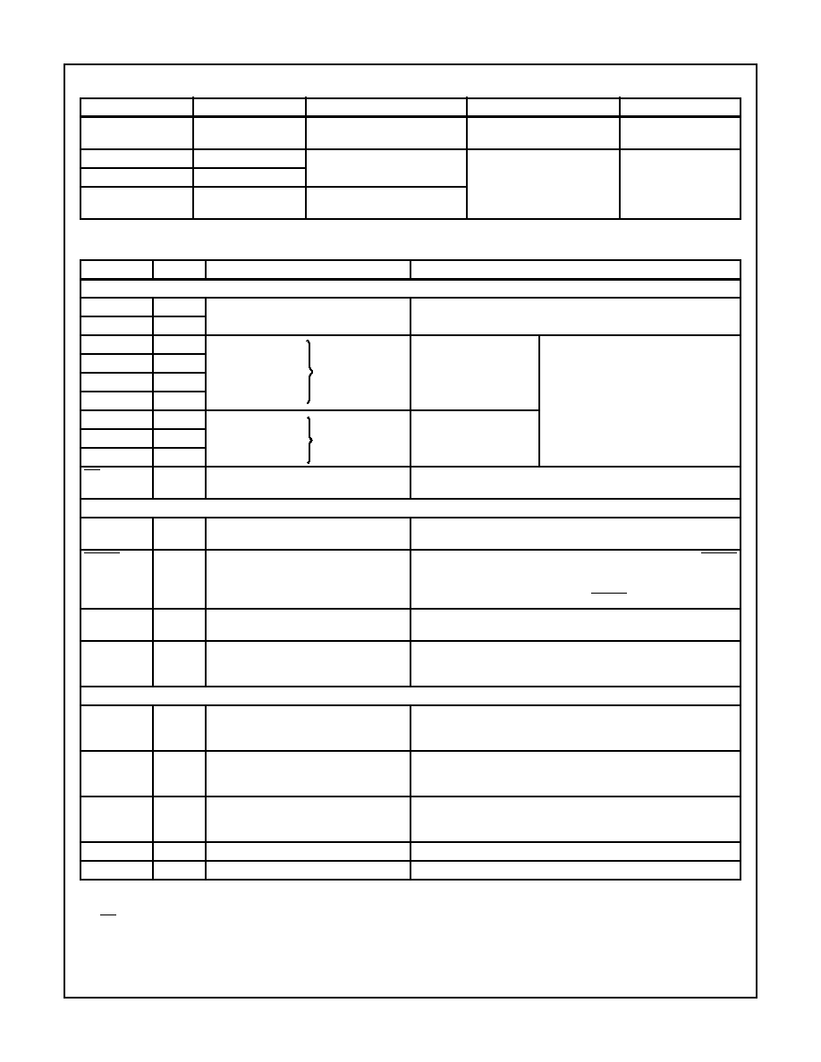
Ordering Information
PART NUMBER
TEMP. RANGE (
o
C)
PACKAGE
NUMBER OF DIGITS
INPUT FORMAT
PKG. NO.
ICM7231BFIJL
-25 to 85
40 Ld CERDIP
8 Digit
Parallel
F40.6
ICM7231BFIPL
-25 to 85
40 Ld PDIP
8 Digit
Parallel
E40.6
ICM7232BFIPL
-25 to 85
40 Ld PDIP
10 Digit
Serial
E40.6
ICM7232CRIPL
-25 to 85
40 Ld PDIP
10 Digit
Serial
E40.6
NOTE:
All versions intended for triplexed LCD displays.
File Number
3161.1
CAUTION: These devices are sensitive to electrostatic discharge; follow proper IC Handling Procedures.
http://www.intersil.com or 407-727-9207
|
Copyright
©
Intersil Corporation 1999
9-20
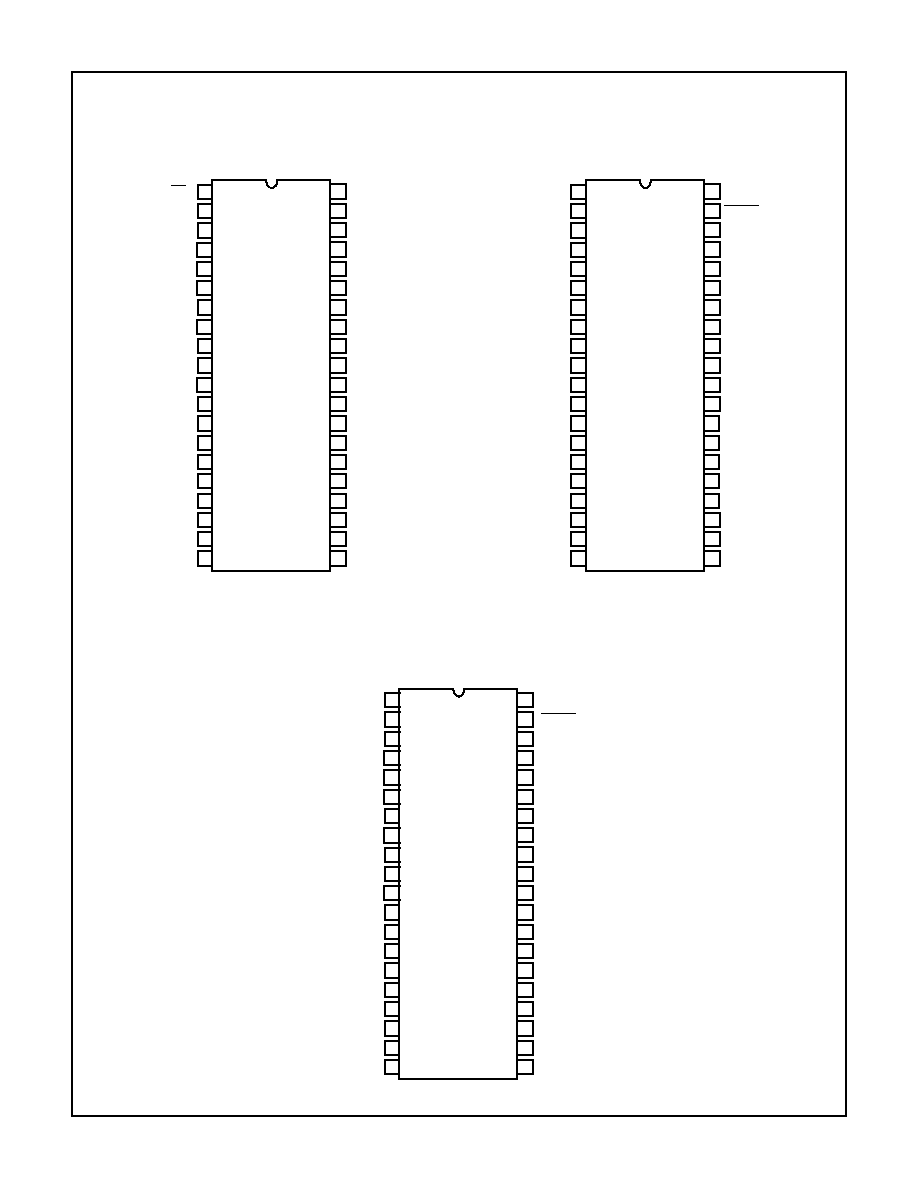
Pinouts
ICM7231BF
(PDIP, CERDIP)
TOP VIEW
ICM7232AF, BF
(PDIP, CERDIP)
TOP VIEW
ICM7232CR
(PDIP)
TOP VIEW
13
1
2
3
4
5
6
7
8
9
10
11
12
14
15
16
17
18
19
20
CS
V
DISP
BP1
BP2
BP3
b
1,
c
1,
an
11
a
1,
g
1,
d
1
f
1,
e
1,
an
21
b
2,
c
2,
an
12
a
2,
g
2,
d
2
f
2,
e
2,
an
22
b
3,
c
3,
an
13
a
3,
g
3,
d
3
f
3,
e
3,
an
23
b
4,
c
4,
an
14
a
4,
g
4,
d
4
f
4,
e
4,
an
24
b
5,
c
5,
an
15
a
5,
g
5,
d
5
f
5,
e
5,
an
25
28
40
39
38
37
36
35
34
33
32
31
30
29
27
26
25
24
23
22
21
V
DD
A2
A1
A0
V
SS
BD3
BD2
BD1
BD0
AN2
AN1
f
8,
a
8,
an
28
a
8,
g
8,
d
8
b
8,
c
8,
an
18
f
7,
e
7,
an
27
a
7,
g
7,
d
7
b
7,
c
7,
an
17
f
6,
e
6,
an
26
a
6,
g
6,
d
6
b
6,
c
6,
an
16
13
1
2
3
4
5
6
7
8
9
10
11
12
14
15
16
17
18
19
20
DATA CLOCK
V
DISP
BP1
BP2
BP3
b
1,
c
1,
an
11
a
1,
g
1,
d
1
f
1,
e
1,
an
21
b
2,
c
2,
an
12
a
2,
g
2,
d
2
f
2,
e
2,
an
22
b
3,
c
3,
an
13
a
3,
g
3,
d
3
f
3,
e
3,
an
23
b
4,
c
4,
an
14
a
4,
g
4,
d
4
f
4,
e
4,
an
24
b
5,
c
5,
an
15
a
5,
g
5,
d
5
f
5,
e
5,
an
25
28
40
39
38
37
36
35
34
33
32
31
30
29
27
26
25
24
23
22
21
V
DD
WRITE INPUT
DATA INPUT
DATA ACCEPTED
V
SS
b
6,
c
6,
an
16
a
6,
g
6,
d
6
f
6,
e
6, an26
b
7,
c
7,
an
17
a
7,
g
7,
d
7
a
9,
g
9,
d
9
f
9,
e
9,
an
29
b
10,
c
10,
an
110
a
10,
g
10,
d
10
f
10,
e
10,
an
210
f
7,
e
7,
an
27
b
8,
c
8,
an
18
a
8,
g
8,
d
8
f
8,
a
8,
an
28
b
9,
c
9,
an
19
OUTPUT
INPUT
13
1
2
3
4
5
6
7
8
9
10
11
12
14
15
16
17
18
19
20
DATA CLOCK
V
DISP
BP1
BP2
BP3
b
1,
c
1,
an
11
a
1,
g
1,
d
1
f
1,
e
1,
an
21
b
2,
c
2,
an
12
a
2,
g
2,
d
2
f
2,
e
2,
an
22
b
3,
c
3,
an
13
a
3,
g
3,
d
3
f
3,
e
3,
an
23
b
4,
c
4,
an
14
a
4,
g
4,
d
4
f
4,
e
4,
an
24
b
5,
c
5,
an
15
a
5,
g
5,
d
5
f
5,
e
5,
an
25
28
40
39
38
37
36
35
34
33
32
31
30
29
27
26
25
24
23
22
21
V
DD
WRITE INPUT
DATA INPUT
DATA ACCEPTED
V
SS
b
6,
c
6,
an
16
a
6,
g
6,
d
6
f
6,
e
6,
an
26
b
7,
c
7,
an
17
a
7,
g
7,
d
7
a
9,
g
9,
d
9
f
9,
e
9,
an
29
b
10,
c
10,
an
110
a
10,
g
10,
d
10
f
10,
e
10,
an
210
f
7,
e
7,
an
27
b
8,
c
8,
an
18
a
8,
g
8,
d
8
f
8,
a
8,
an
28
b
9,
c
9,
an
19
OUTPUT
INPUT
ICM7231, ICM7232
9-21
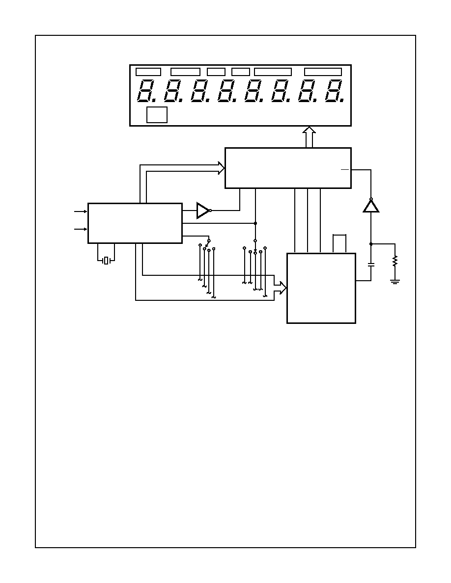
Functional Block Diagrams
ICM7231
NOTE: See Figure 13 for display segment connections.
SEGMENT
LINE
DRIVERS
3 WIDE
OUTPUT
LATCHES
9 WIDE
DATA
DECODER
EN
D8
D7
D6
D5
D4
D3
D2
D1
BP1
BP2
BP3
CS
V
DD
V
H
V
L
V
DISP
ON CHIP
DISPLAY
VOLTAGE
LEVEL
GENERATOR
PIN 2 (INPUT)
ADDRESS INPUTS
DATA INPUTS
f
2,
e
2,
an
22
a
2,
g
2, d2
b
2, c2,
an
12
f
1,
e
1,
an
21
a
1,
g
1,
d
1
b
1,
c
1,
an
11
COMMON
LINE
DRIVERS
DIGIT
ADDRESS
DECODER
DATA INPUT
LATCHES
AN1
BD0
BD2
AN2
BD1
BD3
EN
ADDRESS
INPUT
LATCHES
EN
A2
A1
A0
ONE
SHOT
DISPLAY
TIMING
GENERATOR
9
9
9
9
9
9
9
9
9
9
ICM7231, ICM7232
9-22
ICM7232
NOTE: See Figures 13 and 14 for display segment connections.
Functional Block Diagrams
(Continued)
SEGMENT
LINE
DRIVERS
3 WIDE
OUTPUT
LATCHES
9 WIDE
DATA
DECODER
EN
D10
D7
D6
D5
D4
D3
D2
D1
BP1
BP2
BP3
V
DD
V
H
V
L
V
DISP
ON CHIP
DISPLAY
VOLTAGE
LEVEL
GENERATOR
PIN 2 (INPUT)
SHIFT REGISTER
DATA
COMMON
LINE
DRIVERS
DIGIT
ADDRESS
DECODER
AN1
BD0
BD2
AN2
BD1
BD3
SERIAL INPUT
CONTOL LOGIC
DISPLAY
TIMING
GENERATOR
9
9
D9
D8
9
9
9
9
9
9
9
9
9
INPUT
DATA
CLOCK
WRITE
INPUT
DATA
ACCEPTED
INPUT
OUTPUT
SHIFTS RIGHT TO LEFT
ON RISING EDGE OF DATA CLOCK
CLOCK
DATA
A2
A1
A0
A3
f
2,
e
2,
an
22
a
2,
g
2, d2
b
2, c2,
an
12
f
1,
e
1,
an
21
a
1,
g
1,
d
1
b
1,
c
1,
an
11
ICM7231, ICM7232

9-23
Absolute Maximum Ratings
Thermal Information
Supply Voltage (V
DD
- V
SS
) . . . . . . . . . . . . . . . . . . . . . . . . . . . . 6.5V
Input Voltage (Note 1). . . . . . . . . . . . . . . . . . . . V
SS
- 0.3
V
IN
6.5
Display Voltage (Note 1) . . . . . . . . . . . . . . . . . . . .0.3
V
DISP
+0.3
Operating Conditions
Temperature Range . . . . . . . . . . . . . . . . . . . . . . . . . . -25
o
C to 85
o
C
Thermal Resistance (Typical, Note 2)
JA
(
o
C/W)
JC
(
o
C/W)
PDIP Package . . . . . . . . . . . . . . . . . . .
60
N/A
CERDIP Package . . . . . . . . . . . . . . . .
50
12
Maximum Junction Temperature
Ceramic Package . . . . . . . . . . . . . . . . . . . . . . . . . . . . . . . . 175
o
C
Plastic Package . . . . . . . . . . . . . . . . . . . . . . . . . . . . . . . . . . 150
o
C
Maximum Storage Temperature Range . . . . . . . . . .-65
o
C to 150
o
C
Maximum Lead Temperature (Soldering, 10s) . . . . . . . . . . . . 300
o
C
CAUTION: Stresses above those listed in "Absolute Maximum Ratings" may cause permanent damage to the device. This is a stress only rating and operation
of the device at these or any other conditions above those indicated in the operational sections of this specification is not implied.
NOTES:
1. Due to the SCR structure inherent in these devices, connecting any display terminal or the display voltage terminal to a voltage outside
the power supply to the chip may cause destructive device latchup. The digital inputs should never be connected to a voltage less than
-0.3V below ground, but maybe connected to voltages above V
DD
but not more than 6.5V above V
SS
.
2.
JA
is measured with the component mounted on an evaluation PC board in free air.
Electrical Specifications
V+ = 5V +10%, V
SS
= 0V, T
A
= -25
o
C to 85
o
C, Unless Otherwise Specified
PARAMETER
TEST CONDITIONS
MIN
TYP
MAX
UNITS
Power Supply Voltage, V
DD
4.5
>4
5.5
V
Data Retention Supply Voltage, V
DD
Guaranteed Retention at 2V
2
1.6
-
V
Logic Supply Current, I
DD
Current from V
DD
to Ground Excluding Display.
V
DISP
= 2V
-
30
100
µ
A
Shutdown Total Current, I
S
V
DISP
Pin 2 Open
-
1
10
µ
A
Display Voltage Range, V
DISP
V
SS
V
DISP
V
DD
0
-
V
DD
V
Display Voltage Setup Current, I
DISP
V
DISP
= 2V, Current from V
DD
to V
DISP
On-Chip
-
15
30
µ
A
Display Voltage Setup Resistor Value, R
DISP
One of Three Identical Resistors in String
40
75
-
k
DC Component of Display Signals
(Sample Test Only)
-
1
/
4
1
% (V
DD
- V
DISP
)
Display Frame Rate, f
DISP
See Figure 5
60
90
120
Hz
Input Low Level, V
IL
ICM7231, Pins 30 - 35, 37 - 39, 1
ICM7232, Pins 1, 38, 39 (Note 2)
-
-
0.8
V
Input High Level, V
IH
2.0
-
-
V
Input Leakage, I
ILK
-
0.1
1
µ
A
Input Capacitance, C
IN
-
5
-
pF
Output Low Level, V
OL
Pin 37, ICM7232, I
OL
= 1mA
-
-
0.4
V
Output High Level, V
OH
V
DD
= 4.5V, I
OH
= -500
µ
A
4.1
-
-
V
Operating Temperature Range, T
OP
Industrial Range
-25
-
+85
o
C
AC Specifications
V
DD
= 5V +10% V
SS
= 0V, -25
o
C to 85
o
C
PARAMETER
TEST CONDITIONS
MIN
TYP
MAX
UNITS
PARALLEL INPUT (ICM7231) See Figure 1
Chip Select Pulse Width, t
CS
(Note 1)
500
350
-
ns
Address/Data Setup Time, t
DS
(Note 1)
200
-
-
ns
Address/Data Hold Time, t
DH
(Note 1)
0
-20
-
ns
Inter-Chip Select Time, t
ICS
(Note 1)
3
-
-
µ
s
SERIAL INPUT (ICM7232) See Figures 2, 3
Data Clock Low Time, t
CL
(Note 1)
350
-
-
ns
Data Clock High Time, t
CL
(Note 1)
350
-
-
ns
Data Setup Time, t
DS
(Note 1)
200
-
-
ns
Data Hold Time, t
DH
(Note 1)
0
-20
-
ns
Write Pulse Width, t
WP
(Note 1)
500
350
-
ns
Write Pulse to Clock at Initialization, t
WLL
(Note 1)
1.5
-
-
µ
s
Data Accepted Low Output Delay, t
ODL
(Note 1)
-
200
400
ns
Data Accepted High Output Delay, t
ODH
(Note 1)
-
1.5
3
µ
s
Write Delay After Last Clock, t
CWS
(Note 1)
350
-
-
ns
ICM7231, ICM7232
9-24
Table of Features
TYPE NUMBER
OUTPUT CODE
ANNUNCIATOR LOCATIONS
INPUT
OUTPUT
ICM7231BF
Code B
Both Annunciators on BP3
Parallel Entry, 4-bit Data, 2-bit
Annunciators, 3-bit Address
8 Digits plus
16 Annunciators
ICM7232AF
Hexadecimal
Both Annunciators on BP3
Serial Entry, 4-bit Data, 2-bit
Annunciators, 4-bit Address
10 Digits plus
20 Annunciators
ICM7232BF
Code B
ICM7232CR
Code B
1 Annunciator BP1
1 Annunciator BP3
Terminal Definitions
TERMINAL
PIN NO.
DESCRIPTION
FUNCTION
ICM7231 PARALLEL INPUT NUMERIC DISPLAY
AN1
30
Annunciator 1 Control Bit
High = ON
AN2
31
Annunciator 2 Control Bit
Low = OFF
See Table 3
BD0
32
Least Significant
4-bit Binary
Data Inputs
Input
Data
(See Table 1)
HIGH = Logical One (1)
LOW = Logical Zero (0)
BD1
33
BD2
34
BD3
35
Most Significant
A0
37
Least Significant
3-bit Digit
Address Inputs
Input
Address
(See Table 2)
A1
38
A2
39
Most Significant
CS
1
Data Input Strobe/Chip Select (Note 2)
Trailing (Positive going) edge latches data, causes data input to be
decoded and sent out to addressed digit
ICM7232 SERIAL DATA AND ADDRESS INPUT
Data Input
38
Data+ Address Shift Register Input
HIGH = Logical One (1)
LOW = Logical Zero (O)
WRITE Input
39
Decode, Output, and Reset Strobe
When DATA ACCEPTED Output is LOW, positive going edge of WRITE
causes data in shift register to be decoded and sent to addressed digit,
then shift register and control logic to be reset. When DATA ACCEPTED
Output is HIGH, positive going edge of WRITE triggers reset only.
Data Clock
Input
1
Data Shift Register and Control Logic
Clock
Positive going edge advances data in shift register. ICM7232: Elev-
enth edge resets shift register and control logic.
DATA
ACCEPTED
Output
37
Handshake Output
Output LOW when correct number of bits entered into shift register.
ALL DEVICES
Display
Voltage
V
DlSP
2
Negative end of on-chip resistor string
used to generate intermediate voltage
levels for display. Shutdown Input.
Display voltage control. When open (or less than 1V from V
DD
) chip
is shutdown; oscillator stops, all display pins to V
DD
.
Common
Line Driver
Outputs
3, 4, 5
Drive display commons, or rows
Segment
Line Driver
Outputs
6 - 29
6 - 35
(On ICM7231)
(On ICM7232)
Drive display segments, or columns.
V
DD
40
Chip Positive Supply
V
SS
36
Chip Negative Supply
NOTES:
1. For Design reference only, not 100% tested.
2. CS has a special "mid-level" sense circuit that establishes a test mode if it is held near 3V for several ms. Inadvertent triggering of this
mode can be avoided by pulling it high when inactive, or ensuring frequent activity.
ICM7231, ICM7232
9-25
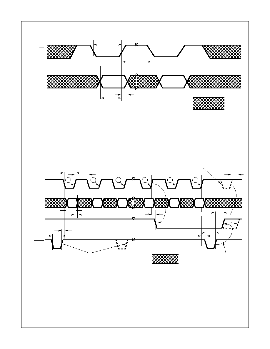
Timing Diagrams
FIGURE 1. ICM7231 INPUT TIMING DIAGRAM
FIGURE 2. ICM7232 ONE DIGIT INPUT TIMING DIAGRAM, WRITING BOTH ANNUNCIATORS
t
DH
t
CS
t
DS
DO NOT CARE
CS
INPUT
DATA
ADDRESS
INPUT
ADDRESS
AND DATA
INPUTS VALID
ADDRESS
AND DATA
INPUTS VALID
t
ICS
DATA
CLOCK
INPUT
(PER BIT
OF DATA)
DATA
INPUT
WRITE
INPUT
RESETS SHIFT REGISTER
AND INPUT CONTROL
LOGIC WHEN DATA
ACCEPTED HIGH
DECODES AND STORES
DATA, RESETS SHIFT
REGISTER AND LOGIC
WHEN DATA ACCEPTED
IS LOW
DO NOT CARE
ELEVENTH CLOCK
WITH NO WRITE PULSE
RESETS SR + LOGIC
t
CI
t
CI
t
DS
t
DH
t
ODL
t
WLL
t
WP
t
CWS
t
WP
DATA
ACCEPTED
OUTPUT
1
2
3
8
9
10
t
ODL
AN2
DATA
VALID
BD0
DATA
VALID
A2
DATA
VALID
t
ODH
A3
DATA
VALID
A1
DATA
VALID
AN1
DATA
VALID
ICM7231, ICM7232
9-26
ICM7231 Family Description
The ICM7231 drives displays with 8 seven-segment digits with
two independent annunciators per digit, accepting six data
bits and three digit address bits from parallel inputs controlled
by a chip select input. The data bits are subdivided into four
binary code bits and two annunciator control bits.
The ICM7232 drives 10 seven-segment digits with two inde-
pendent annunciators per digit. To write into the display, six
bits of data and four bits of digit address are clocked serially
into a shift register, then decoded and written to the display.
Input levels are TTL compatible, and the DATA ACCEPTED
output on the serial input devices will drive one LSTTL load.
The intermediate voltage levels necessary to drive the dis-
play properly are generated by an on-chip resistor string,
and the output of a totally self-contained on-chip oscillator is
used to generate all display timing. All devices in this family
have been fabricated using Intersil' MAXCMOS
Æ
process
and all inputs are protected against static discharge.
Triplexed (
1
/
3
Multiplexed) Liquid Crystal Displays
Figure 4 shows the connection diagram for a typical
7-segment display with two annunciators such as would be
used with an ICM7231 or ICM7232 numeric display driver.
Figure 5 shows the voltage waveforms of the common lines
and one segment line, chosen for this example to be the "a,
g, d" segment line. This line intersects with BP1 to form the
"a" segment, BP2 to form the "g" segment and BP3 to form
the "d" segment. Figure 5 also shows the waveform of the "a,
g, d" segment line for four different ON/OFF combinations of
the "a", "g" and "d" segments. Each intersection (segment or
annunciator) acts as a capacitance from segment line to
common line, shown schematically in Figure 6. Figure 7
shows the voltage across the "g" segment for the same four
combinations of ON/OFF segments used in Figure 5.
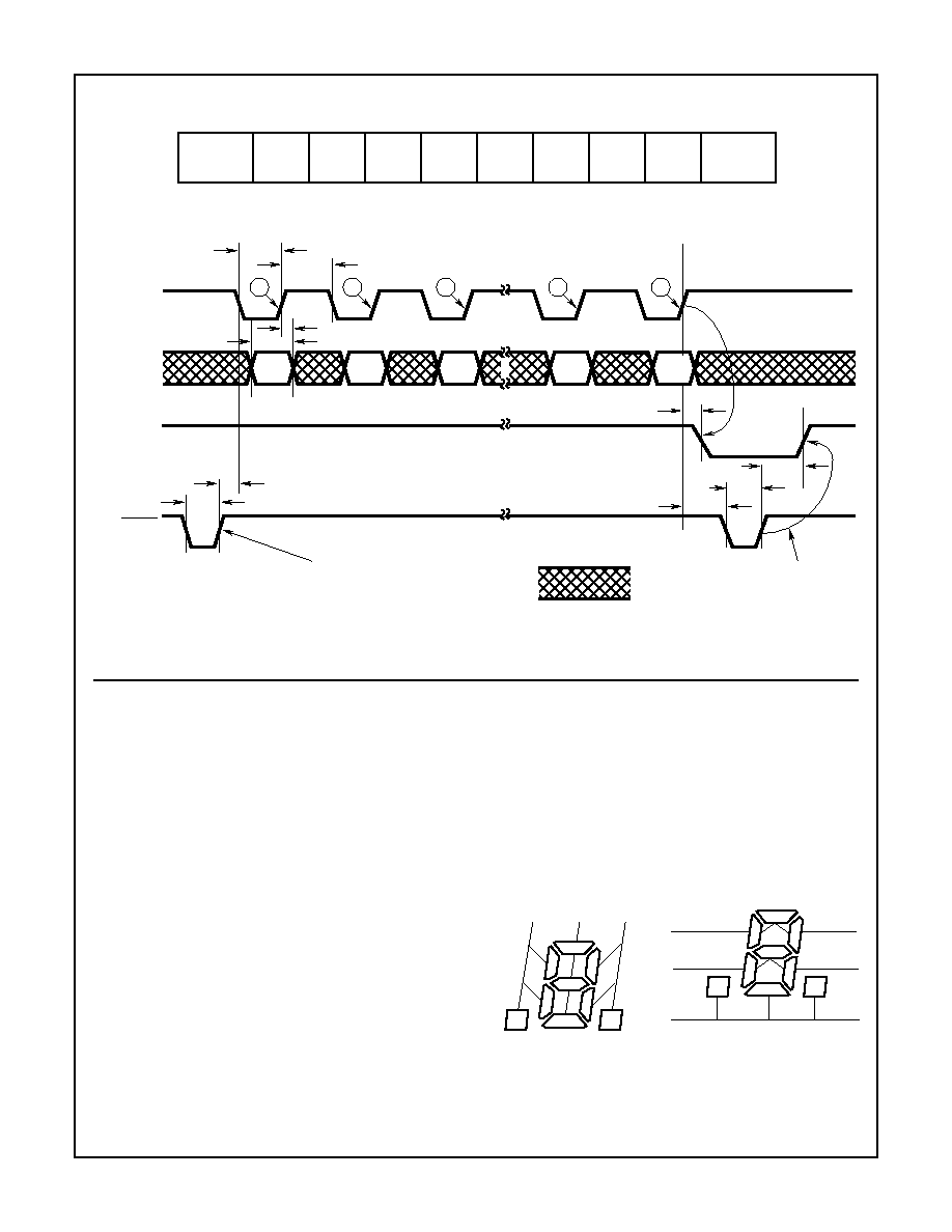
FIGURE 3. ICM7232 INPUT TIMING DIAGRAM, LEAVING BOTH ANNUNCIATORS OFF
Timing Diagrams
DATA
CLOCK
INPUT
DATA
INPUT
WRITE
INPUT
RESETS SHIFT REGISTER
AND INPUT CONTROL
LOGIC WHEN DATA
ACCEPTED HIGH
DECODES AND STORES
DATA, RESETS SHIFT
REGISTER AND LOGIC
WHEN DATA ACCEPTED
IS LOW
DO NOT CARE
t
CI
t
CI
t
DS
t
DH
t
WLL
t
WP
DATA
ACCEPTED
OUTPUT
1
2
3
7
8
BD0
DATA
VALID
t
CWS
t
WP
t
ODH
t
ODI
BD1
DATA
VALID
BD2
DATA
VALID
A2
DATA
VALID
A3
DATA
VALID
AN1
ENTER
FIRST
AN2
BD0
BD1
BD2
BD3
A0
A1
A2
A3
ENTER
LAST
ICM7232 WRITE ORDER
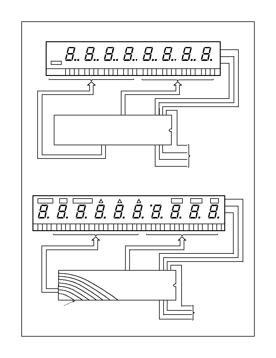
a
b
c
d
f
g
e
BP1
BP2
BP3
an
2
an
1
BACKPLANE CONNECTIONS
a
b
c
d
f
g
e
SEGMENT LINES
an
2
an
1
SEGMENT LINE CONNECTIONS
FIGURE 4. CONNECTION DIAGRAMS FOR TYPICAL
7-SEGMENT DISPLAYS
ICM7231, ICM7232
MAXCMOS
Æ
is a registered trademark of Intersil Corporation.
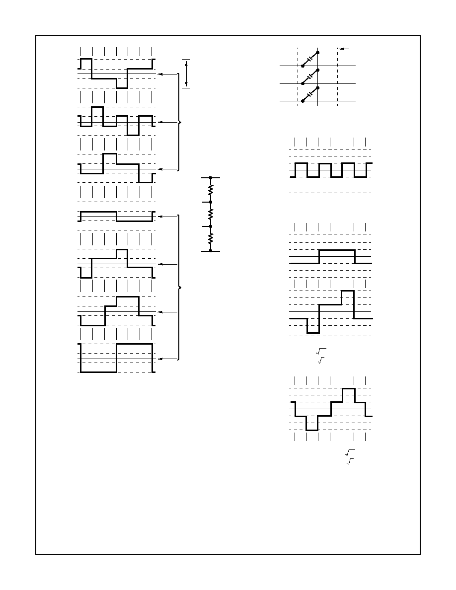
9-27
The degree of polarization of the liquid crystal material and
thus the contrast of any intersection depends on the RMS
voltage across the intersection capacitance. Note from
Figure 7 that the RMS OFF voltage is always V
P
/3 and that
the RMS ON voltage is always 1.92V
PEAK
/3.
For a
1
/
3
multiplexed LCD, the ratio of RMS ON to OFF
voltages is fixed at 1.92, achieving adequate display contrast
with this ratio of applied RMS voltage makes some demands
on the liquid crystal material used.
V
DD
V
H
V
L
V
DISP
V
DD
V
H
V
L
V
DISP
V
DD
V
H
V
L
V
DISP
V
DD
V
H
V
L
V
DISP
V
DD
V
H
V
L
V
DISP
V
DD
V
H
V
L
V
DISP
V
DD
V
H
V
L
V
DISP
BP1
BP2
BP3
ALL ON
a
,
g
ON
d OFF
a
SEGMENT
ON
a
,
d
OFF
SEGMENT
LINE
ALL OFF
1
2
3
1¥
2¥
3¥
V
P
V
DD
V
H
V
L
V
DISP
ON CHIP
RESISTOR
STRING
~
75k
~
75k
~
75k
INPUT
COMMON LINE
WAVEFORMS
TYPICAL
SEGMENT LINE
WAVEFORMS
PIN 2
NOTES:
1.
1,
2,
3, - BP High with Respect to Segment.
2.
1¥,
2¥,
3¥, - BP Low with Respect to Segment.
3. BP1 Active during
1, and
1¥.
4. BP2 Active during
2, and
2¥.
5. BP3 Active during
3, and
3¥.
FIGURE 5. DISPLAY VOLTAGE WAVEFORMS
BP1
BP2
BP3
f
e
an
2
a
g
d
b
c
an
1
SEGMENT
LINES
FIGURE 6. DISPLAY SCHEMATIC
1
2
3
1¥
2¥
3¥
ALL ON
a, g ON
d OFF
a SEGMENT
ON
a, d OFF
ALL OFF
+VP
0
-VP
+VP
0
-VP
+VP
0
-VP
+VP
0
-VP
VP = (V+) - VDISP
V
RMS
VP
3
--------
V
RMS
OFF
=
=
V
RMS
11
3
----------
VP
3
--------
◊
V
RMS
ON
=
=
NOTES:
1.
1,
2,
3, - BP High with Respect to Segment.
2.
1¥,
2¥,
3¥, - BP Low with Respect to Segment.
3. BP1 Active during
1, and
1¥.
4. BP2 Active during
2, and
2¥.
5. BP3 Active during
3, and
3¥.
FIGURE 7. VOLTAGE WAVEFORMS ON SEGMENT g(V
G
)
Voltage Contrast Ratio
V
RMS
ON
V
RMS
OFF
------------------------------
11
3
----------
1.92
=
=
=
ICM7231, ICM7232
9-28
Figure 8 shows the curve of contrast versus applied RMS volt-
age for a liquid crystal material tailored for V
PEAK
= 3.1V, a
typical value for
1
/
3
multiplexed displays in calculators. Note
that the RMS OFF voltage V
PEAK
/3
1V is just below the
"threshold" voltage where contrast begins to increase. This
places the RMS ON voltage at 2.1V, which provides about
85% contrast when viewed straight on.
All members of the ICM7231 and ICM7232 family use an internal
resistor string of three equal value resistors to generate the volt-
ages used to drive the display. One end of the string is connected
on the chip to V
DD
and the other end (user input) is available at
pin 2 (V
DISP
) on each chip. This allows the display voltage input
(V
DISP
) to be optimized for the particular liquid crystal material
used. Remember that V
PEAK
= V
DD
- V
DISP
and should be
three times the threshold voltage of the liquid crystal material
used. Also it is very important that pin 2 never be driven below
V
SS
. This can cause device latchup and destruction of the chip.
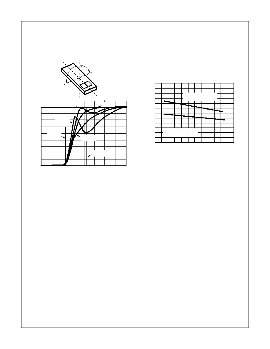
Temperature Effects and Temperature Compensation
The performance of the LCD material is affected by tempera-
ture in two ways. The response time of the display to changes
of applied RMS voltage gets longer as the display tempera-
ture drops. At very low temperatures (-20
o
C) some displays
may take several seconds to change a new character after the
new information appears at the outputs. However, for most
applications above 0
o
C this will not be a problem with avail-
able multiplexed LCD materials, and for low-temperature
applications, high-speed liquid crystal materials are available.
At high temperature, the effect to consider deals with plastic
materials used to make the polarizer.
Some polarizers become soft at high temperatures and per-
manently lose their polarizing ability, thereby seriously
degrading display contrast. Some displays also use sealing
materials unsuitable for high temperature use. Thus, when
specifying displays the following must be kept in mind: liquid
crystal material, polarizer, and seal materials.
A more important effect of temperature is the variation of
threshold voltage. For typical liquid crystal materials suitable for
multiplexing, the peak voltage has a temperature coefficient of -7
to -14mV/
o
C. This means that as temperature rises, the thresh-
old voltage goes down. Assuming a fixed value for V
P
, when the
threshold voltage drops below V
PEAK
/3 OFF segments begin to
be visible. Figure 9 shows the temperature dependence of peak
voltage for the same liquid crystal material of Figure 8.
For applications where the display temperature does not
vary widely, V
PEAK
may be set at a fixed voltage chosen to
make the RMS OFF voltage, V
PEAK
/3, just below the thresh-
old voltage at the highest temperature expected. This will
prevent OFF segments turning ON at high temperature (this
at the cost of reduced contrast for ON segments at low
temperatures).
For applications where the display temperature may vary to
wider extremes, the display voltage V
DISP
(and thus V
PEAK
)
may require temperature compensation to maintain sufficient
contrast without OFF segments becoming visible.
Display Voltage and Temperature Compensation
These circuits allow control of the display peak voltage by
bringing the bottom of the voltage divider resistor string out at
pin 2. The simplest means for generating a display voltage
suitable to a particular display is to connect a potentiometer
from pin 2 to V
SS
as shown in Figure 10. A potentiometer with
a maximum value of 200k
should give sufficient range of
adjustment to suit most displays. This method for generating
display voltage should be used only in applications where the
temperature of the chip and display won't vary more than
±
5
o
C (
±
9
o
F), as the resistors on the chip have a positive tem-
perature coefficient, which will tend to increase the display
peak voltage with an increase in temperature. The display
voltage also depends on the power supply voltage, leading to
tighter tolerances for wider temperature ranges.
APPLIED VOLTAGE (V
RMS
)
CONTRAST (%)
100
90
80
70
60
50
40
30
20
10
0
T
A
= 25
o
C
= -10
o
= -30
o
= 0
V
ON
= 2.1V
0
1
2
3
4
= +10
o
V
OFF
=
1.1V
RMS
0-
0+
FIGURE 8. CONTRAST vs APPLIED RMS VOLTAGE
AMBIENT TEMPERATURE (
o
C)
6
5
4
3
2
1
0
-10
0
10
20
30
40
50
PEAK VOLTAGE FOR
90% CONTRAST (ON)
PEAK VOLTAGE FOR
10% CONTRAST (OFF)
PEAK V
O
L
T
A
GE
FIGURE 9. TEMPERATURE DEPENDENCE OF LC THRESHOLD
ICM7231, ICM7232

9-29
Figure 11A shows another method of setting up a display
voltage using five silicon diodes in series. These diodes,
1N914 or equivalent, will each have a forward drop of
approximately 0.65V, with approximately 20
µ
A flowing
through them at room temperature. Thus, 5 diodes will give
3.25V, suitable for a 3V display using the material properties
shown in Figures 4 and 5. For higher voltage displays, more
diodes may be added. This circuit provides reasonable
temperature compensation, as each diode has a negative
temperature coefficient of -2mV/
o
C; five in series gives
-10mV/
o
C, not far from optimum for the material described.
The disadvantage of the diodes in series is that only integral
multiples of the diode voltage can be achieved. The diode
voltage multiplier circuit shown in Figure 11B allows fine-
tuning the display voltage by means of the potentiometer; it
likewise provides temperature compensation since the tem-
perature coefficient of the transistor base-emitter junction
(about -2mV/
o
C) is also multipled. The transistor should have
a beta of at least 100 with a collector current of 10
µ
A. The
inexpensive 2N2222 shown in the figure is a suitable device.
For battery operation, where the display voltage is generally the
same as the battery voltage (usually 3 - 4.5V), the chip may be
operated at the display voltage, with V
DlSP
connected to V
SS
.
The inputs of the chip are designed such that they may be
driven above V
DD
without damaging the chip. This allows, for
example, the chip and display to operate at a regulated 3V, and
a microprocessor driving its inputs to operate with a less well
controlled 5V supply. (The inputs should not be driven more
than 6.5V above GND under any circumstances.) This also
allows temperature compensation with the ICL7663S, as
shown in Figure 12. This circuit allows independent adjustment
of both voltage and temperature compensation.
Description Of Operation
Parallel Input Of Data And Address (ICM7231)
The parallel input structure of the ICM7231 device is
organized to allow simple, direct interfacing to all micropro-
cessors, (see the Functional Block Diagram). In the
ICM7231, address and data bits are written into the input
latches on the rising edge of the Chip Select input.
The rising edge of the Chip Select also triggers an on-chip
pulse which enables the address decoder and latches the
decoded data into the addressed digit/character outputs. The
timing requirements for the parallel input device are shown in
Figure 1, with the values for setup, hold, and pulse width times
shown in the AC Specifications section. Note that there is a
minimum time between Chip Select pulses; this is to allow suf-
ficient time for the on-chip enable pulse to decay, and ensures
that new data doesn't appear at the decoder inputs before the
decoded data is written to the outputs.
Serial Input Of Data And Address (ICM7232)
The ICM3232 trades six pins used as data inputs on the
ICM7231 for six more segment lines, allowing two more
9-segment digits. This is done at the cost of ease in interfac-
ing, and requires that data and address information be
entered serially. Refer to Functional Block Diagram and tim-
ing diagrams, Figures 2 and 3. The interface consists of four
pins: DATA Input, DATA CLOCK Input, WRITE Input and
DATA ACCEPTED Output. The data present at the DATA
Input is clocked into a shift register on the rising edge of the
OPEN
200k
10nF
+5
ICM7231
ICM7232
V
DISP
2
40
36
FIGURE 10. SIMPLE DISPLAY VOLTAGE ADJUSTMENT
V
DD
40k
10nF
+5
ICM7231
ICM7232
V
DISP
2
40
36
1N914
DIODES
FIGURE 11A. STRING OF DIODES
V
DD
40k
10nF
+5
ICM7231
ICM7232
V
DISP
2
40
36
200k
POTENTIOMETER
2N2222
FIGURE 11B. TRANSISTOR-MULTIPLIER
FIGURE 11. DIODE-BASED TEMPERATURE COMPENSATION
V
IN
+
V
OUT1
V
OUT2
ICL7663S
V
SET
V
TC
GND
DATA BUS
ICM7233
V
DISP
GND
1.8M
300k
2.7M
LOGIC
SYSTEM
PROCESSOR,
+5V
V
DD
ETC.
FIGURE 12. FLEXIBLE TEMPERATURE COMPENSATION
ICM7231, ICM7232
9-30
DATA CLOCK Input signal, and when the correct number of
bits has been shifted into the shift register (8 in the
ICM7232), the DATA ACCEPTED Output goes low. Following
this, a low-going pulse at the WRITE input will trigger the
chip to decode the data and store it in the output latches of
the addressed digit/character. After the data is latched at the
outputs, the shift register and the control logic are reset,
returning the DATA ACCEPTED Output high. After this occurs,
a pulse at the WRITE input will not change the outputs, but
will reset the control logic and shift register, assuring that each
data bit will be entered into the correct position in the shift reg-
ister depending on subsequent DATA CLOCK inputs.
The shift register and control logic will also be reset if too
many DATA CLOCK INPUT edges are received; this pre-
vents incorrect data from being decoded. In the ICM7232,
the eleventh clock resets the shift register and control logic.
The recommended procedure for entering data is shown in
the serial input timing diagram, Figure 2. First, when DATA
ACCEPTED is high, send a WRITE pulse. This resets the
shift register and control logic and initializes the chip for the
data input sequence. Next clock in the appropriate number
of correct data and address bits. The DATA ACCEPTED Out-
put may be monitored if desired, to determine when the chip
is ready to output the decoded data. When the correct num-
ber of bits has been entered, and the DATA ACCEPTED Out-
put is low, a pulse at WRITE will cause the data to be
decoded and stored in the latches of the addressed
digit/character. The shift register and control logic are reset,
causing DATA ACCEPTED to return high, and leaving the
chip ready to accept data for the next digit/character.
Note that for the ICM7232 the eleventh clock resets the shift
register and control logic, but the DATA ACCEPTED Output
goes low after the eighth clock. This allows the user to
abbreviate the data to eight bits, which will write the correct
character to the 7-segment display, but will leave the annun-
ciators off, as shown in Figure 3.
If only AN2 is to be turned on, nine bits are clocked in; if AN1
is to be turned on, all ten bits are used.
The DATA ACCEPTED Output will drive one low-power
Schottky TTL input, and has equal current drive capability
pulling high or low.
Note that in the serial Input devices, it is possible to address
digits/characters which don't exist. As shown in Table 2
when an incorrect address is applied together with a WRITE
pulse, none of the outputs will be changed.
Display Fonts and Output Codes
The standard versions of the ICM7231 and ICM7232 chips are
programmed to drive a 7-segment display plus two annuncia-
tors per digit. See Table 3 for annunciator input controls.
The "A" and "B" suffix chips place both annunciators on BP3.
The display connections for one digit of this display are
shown in Figure 13. The "A" devices decode the input data
into a hexadecimal 7-segment output, while the "B" devices
supply Code B outputs (see Table 1).
The "C" devices place the left hand annunciator on BP1 and
the right hand annunciator (usually a decimal point) on BP3.
(See Figure 14). The "C" devices provide only a "Code B"
output for the 7 segments.
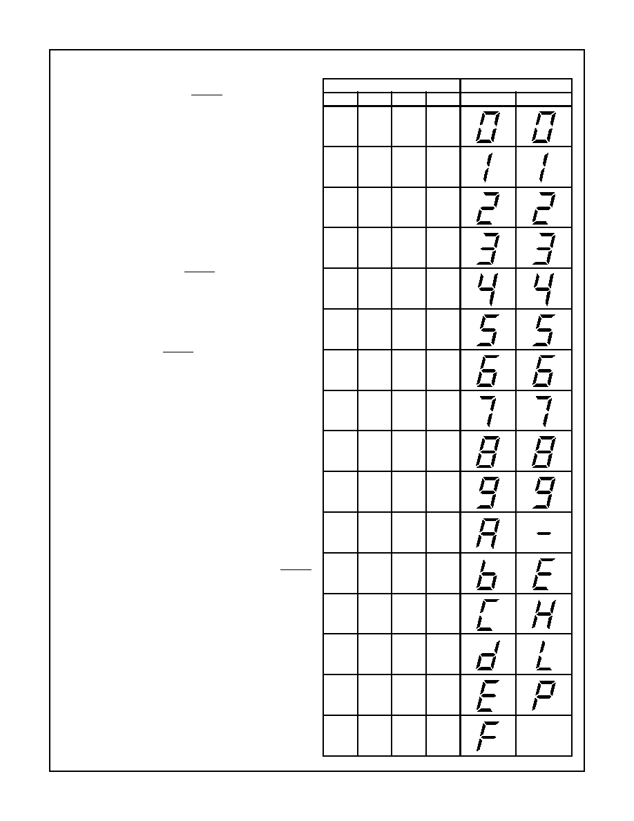
TABLE 1. BlNARY DATA DECODING ICM7231 AND ICM7232
CODE INPUT
DISPLAY OUTPUT
BD3
BD2
BD1
BD0
HEX
CODE B
0
0
0
0
0
0
0
1
0
0
1
0
0
0
1
1
0
1
0
0
0
1
0
1
0
1
1
0
0
1
1
1
1
0
0
0
1
0
0
1
1
0
1
0
1
0
1
1
1
1
0
0
1
1
0
1
1
1
1
0
1
1
1
1
BLANK
ICM7231, ICM7232

9-31
)
Compatible Displays
Compatible displays are manufactured by: G.E. Displays
Inc., Beechwood, Ohio (216) 831-8100 (#356E3R99HJ)
Epson America Inc., Torrance CA
(Model Numbers LDB726/7/8).
Seiko Instruments USA Inc., Torrance CA
(Custom Displays)
Crystaloid, Hudson, OH
TABLE 2. ADDRESS DECODING (ICM7231 AND ICM7232)
CODE INPUT
DISPLAY
OUTPUT
ICM7232
ONLY
A3
A2
A1
A0
DIGIT
SELECTED
0
0
0
0
D1
0
0
0
1
D2
0
0
1
0
D3
0
0
1
1
D4
0
1
0
0
D5
0
1
0
1
D6
0
1
1
0
D7
0
1
1
1
D8
1
0
0
0
D9
1
0
0
1
D10
1
0
1
0
NONE
1
0
1
1
NONE
1
1
0
0
NONE
1
1
0
1
NONE
1
1
1
0
NONE
1
1
1
1
NONE
TABLE 3. ANNUNClATOR DECODING
CODE
INPUT
DISPLAY OUTPUT
AN2
AN1
ICM7231A AND
ICM7231B
ICM7232A AND
ICM7232B
BOTH
ANNUNCIATORS
ON BP3
ICM7231C
ICM7232C
an2
ANNUNCIATOR
BP1
an1
ANNUNClATOR
BP3
0
0
0
1
1
0
1
1
a
b
c
d
f
g
e
BP1
BP2
BP3
an
2
an
1
BACKPLANE CONNECTIONS
SEGMENT LINES
SEGMENT LINE CONNECTIONS
FIGURE 13. ICM7231 AND ICM7232 DISPLAY FONTS ("A" AND
"B" SUFFIX VERSIONS
a
b
c
d
f
g
e
SEGMENT LINES
BP1
BP2
BP3
an
2
an
1
(NOTE 1)
BACKPLANE CONNECTIONS
SEGMENT LINES
(NOTE 1)
SEGMENT LINE CONNECTIONS
NOTE:
1. Annunciators can be:
,
,
,
-arrows that
point to information printed around the display opening etc.,
whatever the designer display opening etc., whatever the de-
signer chooses to incorporate in the liquid crystal display.
FIGURE 14. ICM7231 DISPLAY FONTS ("C" SUFFIX VERSIONS)
STOP
GO
ICM7231, ICM7232
9-32
Typical Applications
NOTE: The annunciators show function and the decimal points indicate the range of the current operation. the system can be efficiently
battery operated.
FIGURE 15. 10MHz FREQUENCY/PERIOD POINTER WITH LCD DISPLAY
PERIOD
INTERVAL
TEST
FREQ. RATIO
FREQUENCY
UNIT
OVER
RANGE
INPUT A
INPUT B
ICM7226A
D1 - D8
BCD
DP
FUNCTION
RANGE
CD4532
GS
D0 - D7
+5V
CS
ICM7231CF
BD0 - 3
AN2
AN1
A0
A1
A2
Q0
Q1
Q2
E1
V+
1
µ
F
10K
27
ICM7231, ICM7232
9-33
FIGURE 16. "FORWARD" PIN ORIENTATION AND DISPLAY CONNECTIONS
FIGURE 17. "REVERSE" PIN ORIENTATION AND DISPLAY CONNECTIONS
Typical Applications
(Continued)
X Y Z
X Y Z
X Y Z
X Y Z
X Y Z
X Y Z
X Y Z
X Y Z
ICM7231AF AND ICM7231BF
TOP VIEW
COM 1
COM 2
COM 3
TO INPUT
D8
D7
D6
D5
D4
D3
D2
D1
X Y Z
X Y Z
X Y Z
X Y Z
X Y Z
X Y Z
X Y Z
X Y Z
ICM7232CR
TOP VIEW
COM 1
COM 2
COM 3
TO INPUT
D8
D7
D6
D5
D4
D3
D2
D1
PCB TRACES UNDER PACKAGE
SELECT
NO
FORWARD
STOP
X Y Z
X Y Z
WAIT
GO
D9
D10
ICM7231, ICM7232

9-34
All Intersil semiconductor products are manufactured, assembled and tested under ISO9000 quality systems certification.
Intersil products are sold by description only. Intersil Corporation reserves the right to make changes in circuit design and/or specifications at any time without
notice. Accordingly, the reader is cautioned to verify that data sheets are current before placing orders. Information furnished by Intersil is believed to be accurate
and reliable. However, no responsibility is assumed by Intersil or its subsidiaries for its use; nor for any infringements of patents or other rights of third parties which
may result from its use. No license is granted by implication or otherwise under any patent or patent rights of Intersil or its subsidiaries.
For information regarding Intersil Corporation and its products, see web site http://www.intersil.com
Sales Office Headquarters
NORTH AMERICA
Intersil Corporation
P. O. Box 883, Mail Stop 53-204
Melbourne, FL 32902
TEL: (407) 724-7000
FAX: (407) 724-7240
EUROPE
Intersil SA
Mercure Center
100, Rue de la Fusee
1130 Brussels, Belgium
TEL: (32) 2.724.2111
FAX: (32) 2.724.22.05
ASIA
Intersil (Taiwan) Ltd.
Taiwan Limited
7F-6, No. 101 Fu Hsing North Road
Taipei, Taiwan
Republic of China
TEL: (886) 2 2716 9310
FAX: (886) 2 2715 3029
ICM7231, ICM7232