8-163
November 1996
ICM7242
Long Range Fixed Timer
Features
∑ Replaces the 2242 in Most Applications
∑ Timing From Microseconds to Days
∑ Cascadable
∑ Monostable or Astable Operation
∑ Wide Supply Voltage Range . . . . . . . . . . . . . . 2V to 16V
∑ Low Supply Current . . . . . . . . . . . . . . . . . . . 115
µ
A at 5V
Description
The ICM7242 is a CMOS timer/counter circuit consisting of
an RC oscillator followed by an 8-bit binary counter. It will
replace the 2242 in most applications, with a significant
reduction in the number of external components.
Three outputs are provided. They are the oscillator output,
and buffered outputs from the first and eighth counters.
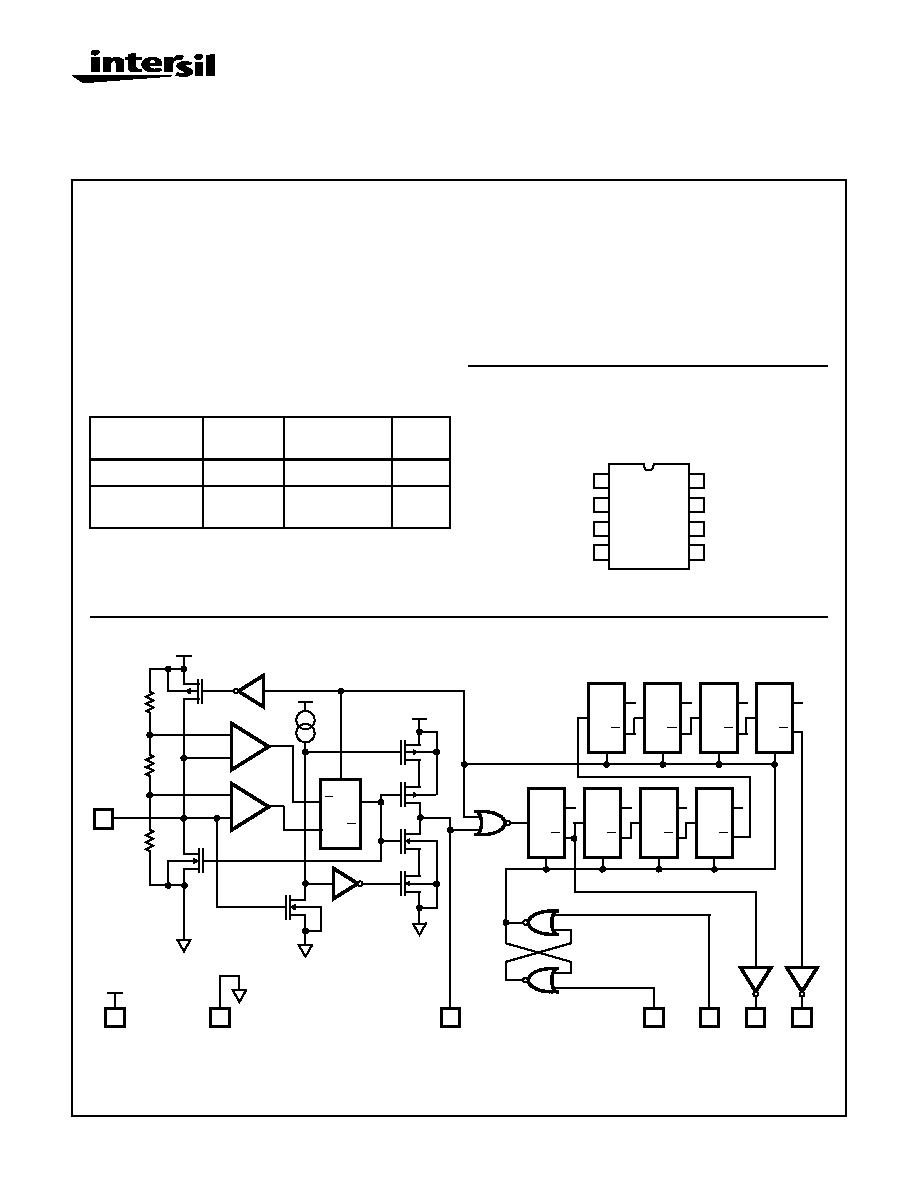
Pinout
ICM7242
(PDIP, SOIC)
TOP VIEW
Functional Diagram
Ordering Information
PART NUMBER
(BRAND)
TEMP.
RANGE (
o
C)
PACKAGE
PKG.
NO.
ICM7242IPA
-25 to 85
8 Ld PDIP
E8.3
ICM7242CBA
(7242CBA)
0 to 70
8 Ld SOIC
M8.15
V
DD
˜
2 OUT
˜
128/256 OUT
V
SS
1
2
3
4
8
7
6
5
TB I/O
RC
TRIGGER
RESET
+
-
+
-
R
Q
Q
S
R
1
4
8
5
6
2
3
TRIGGER
RESET
˜
2 OUT
TB I/O
V
SS
Q
Q
S
CL
Q
Q
S
CL
Q
Q
S
CL
Q
Q
S
CL
˜
128/256
OUTPUT
R
1
50K
R
2
86K
R
3
50K
V
DD
RC
7
Q
Q
S
CL
Q
Q
S
CL
Q
Q
S
CL
Q
Q
S
CL
File Number
2866.2
CAUTION: These devices are sensitive to electrostatic discharge; follow proper IC Handling Procedures.
1-888-INTERSIL or 321-724-7143 | Copyright © Intersil Corporation 1999
8-164
Absolute Maximum Ratings
Thermal Information
Supply Voltage (V
DD
to V
SS
) . . . . . . . . . . . . . . . . . . . . . . . . . . . 18V
Input Voltage (Note 1)
Terminals (Pins 5, 6, 7, 8) . . . . . . . . . .(V
SS
-0.3V) to (V
DD
+0.3V)
Continuous Output Current (Each Output) . . . . . . . . . . . . . . . . 50mA
Operating Conditions
Temperature Range
ICM7242I . . . . . . . . . . . . . . . . . . . . . . . . . . . . . . . . -25
o
C to 85
o
C
ICM7242C. . . . . . . . . . . . . . . . . . . . . . . . . . . . . . . . . .0
o
C to 70
o
C
Thermal Resistance (Typical, Note 2)
JA
(
o
C/W)
PDIP Package . . . . . . . . . . . . . . . . . . . . . . . . . . . . .
100
SOIC Package . . . . . . . . . . . . . . . . . . . . . . . . . . . . .
160
Maximum Storage Temperature Range . . . . . . . . . -65
o
C to 150
o
C
Maximum Junction Temperature (Plastic Package) . . . . . . . . 150
o
C
Maximum Lead Temperature (Soldering 10s) . . . . . . . . . . . . . 300
o
C
(SOIC - Lead Tips Only)
CAUTION: Stresses above those listed in "Absolute Maximum Ratings" may cause permanent damage to the device. This is a stress only rating and operation
of the device at these or any other conditions above those indicated in the operational sections of this specification is not implied.
NOTES:
1. Due to the SCR structure inherent in the CMOS process, connecting any terminal to voltages greater than V
DD
or less than V
SS
may cause
destructive device latchup. For this reason, it is recommended that no inputs from external sources not operating on the same supply be
applied to the device before its supply is established and, that in multiple supply systems, the supply to the ICM7242 be turned on first.
2.
JA
is measured with the component mounted on an evaluation PC board in free air.
Electrical Specifications
V
DD
= 5V, T
A
= 25
o
C, R = 10k
, C = 0.1
µ
F, V
SS
= 0V, Unless Otherwise Specified
PARAMETER
SYMBOL
TEST CONDITIONS
MIN
TYP
MAX
UNITS
Guaranteed Supply Voltage
V
DD
2
-
16
V
Supply Current
I
DD
Reset
-
125
-
µ
A
Operating, R = 10k
, C = 0.1
µ
F
-
340
800
µ
A
Operating, R = 1M
, C = 0.1
µ
F
-
220
600
µ
A
TB Inhibited, RC Connected to V
SS
-
225
-
µ
A
Timing Accuracy
-
5
-
%
RC Oscillator Frequency Temperature
Drift
f/
t
Independent of RC Components
-
250
-
ppm/
o
C
Time Base Output Voltage
V
OTB
I
SOURCE
= 100
µ
A
-
3.5
-
V
I
SINK
= 1.0mA
-
0.40
-
V
Time Base Output Leakage Current
I
TBLK
RC = Ground
-
-
25
µ
A
Trigger Input Voltage
V
TRIG
V
DD
= 5V
-
1.6
2.0
V
V
DD
= 15V
-
3.5
4.5
V
Reset Input Voltage
V
RST
V
DD
= 5V
-
1.3
2.0
V
V
DD
= 15V
-
2.7
4.0
V
Trigger/Reset Input Current
I
TRIG
, I
RST
-
10
-
µ
A
Max Count Toggle Rate
f
T
V
DD
= 2V
Counter/Divider Mode
-
1
-
MHz
V
DD
= 5V
2
6
-
MHz
V
DD
= 15V
-
13
-
MHz
50% Duty Cycle Input with Peak to Peak
Voltages Equal to V
DD
and V
SS
Output Saturation Voltage
V
SAT
All Outputs Except TB Output V
DD
= 5V,
I
OUT
= 3.2mA
-
0.22
0.4
V
Output Sourcing Current
I
SOURCE
V
DD
= 5V Terminals 2 and 3, V
OUT
= 1V
-
300
-
µ
A
MIN Timing Capacitor (Note 3)
C
T
10
-
-
pF
Timing Resistor Range (Note 3)
R
T
V
DD
= 2 - 16V
1K
-
22M
NOTE:
3. For design only, not tested.
ICM7242

8-165
Test Circuit
Application Information
Operating Considerations
Shorting the RC terminal or output terminals to V
DD
may
exceed dissipation ratings and/or maximum DC current limits
(especially at high supply voltages).
There is a limitation of 50pF maximum loading on the TB I/O
terminal if the timebase is being used to drive the counter
section. If higher value loading is used, the counter sections
may miscount.
For greatest accuracy, use timing component values shown
in Figure 8. For highest frequency operation it will be desir-
able to use very low values for the capacitor; accuracy will
decrease for oscillator frequencies in excess of 200kHz.
The timing capacitor should be connected between the RC
pin and the positive supply rail, V
DD
, as shown in Figure 1.
When system power is turned off, any charge remaining on
the capacitor will be discharged to ground through a large
internal diode between the RC node and V
SS
. Do NOT refer-
ence the timing capacitor to ground, since there is no high
current path in this direction to safely discharge the capacitor
when power is turned off. The discharge current from such a
configuration could potentially damage the device.
When driving the counter section from an external clock, the
optimum drive waveform is a square wave with an amplitude
equal to the supply voltage. If the clock is a very slow ramp
triangular, sine wave, etc., it will be necessary to "square up"
the waveform; this can be done by using two CMOS invert-
ers in series, operating from the same supply voltage as the
ICM7242.
The ICM7242 is a non-programmable timer whose principal
applications will be very low frequency oscillators and long
range timers; it makes a much better low frequency oscilla-
tor/timer than a 555 or ICM7555, because of the on-chip
8-bit counter. Also, devices can be cascaded to produce
extremely low frequency signals.
Because outputs will not be ANDed, output inverters are
used instead of open drain N-Channel transistors, and the
external resistors used for the 2242 will not be required for
the ICM7242. The ICM7242 will, however, plug into a socket
for the 2242 having these resistors.
The timing diagram for the ICM7242 is shown in Figure 1.
Assuming that the device is in the RESET mode, which
occurs on power up or after a positive signal on the RESET
terminal (if TRIGGER is low), a positive edge on the trigger
input signal will initiate normal operation. The discharge
transistor turns on, discharging the timing capacitor C, and
all the flip-flops in the counter chain change states. Thus, the
outputs on terminals 2 and 3 change from high to low states.
After 128 negative timebase edges, the
˜
2
8
output returns to
the high state.
NOTE:
4.
˜
2
1
and
˜
2
8
outputs are inverters and have active pullups.
V
DD
˜
2
1
(RC/2) OUTPUT
1
2
3
4
8
7
6
5
TIME BASE INPUT/OUTPUT
R
TRIGGER
RESET
C
V
DD
˜
2
8
(RC/256) OUTPUT
TIME BASE PERIOD = 1.0RC;
1s = 1M
x 1
µ
F
TRIGGER INPUT
(TERMINAL 6)
TIMEBASE INPUT
(TERMINAL 8)
˜
2 OUTPUT
(TERMINAL 2)
˜
128/256 OUTPUT
(TERMINAL 3) (ASTABLE
OR "FREE RUN" MODE)
˜
128/256 OUTPUT
(TERMINAL 3)
OR "ONE SHOT" MODE)
(MONOSTABLE
128RC
128RC
128RC
FIGURE 1. TIMING DIAGRAMS OF OUTPUT WAVEFORMS
FOR THE ICM7242 (COMPARE WITH FIGURE 5)
OUTPUTS
1
2
3
4
8
7
6
5
3
/
4
(V+)
V
DD
f
IN
V
DD
f
IN/2
f
IN/256
1
/
4
(V+)
FIGURE 2. USING THE ICM7242 AS A RIPPLE COUNTER
(DIVIDER)
ICM7242

8-166
To use the 8-bit counter without the timebase, Terminal 7
(RC) should be connected to ground and the outputs taken
from Terminals 2 and 3.
The ICM7242 may be used for a very low frequency square
wave reference. For this application the timing components
are more convenient than those that would be required by a
555 timer. For very low frequencies, devices may be cas-
caded (see Figure 3).
For monostable operation the
˜
2
8
output is connected to the
RESET terminal. A positive edge on TRIGGER initiates the
cycle (NOTE: TRIGGER overrides RESET).
The ICM7242 is superior in all respects to the 2242 except
for initial accuracy and oscillator stability. This is primarily
due to the fact that high value p- resistors have been used
on the ICM7242 to provide the comparator timing points.
By selection of R and C, a wide variety of sequence timing
can be realized. A typical flow chart for a machine tool con-
troller could be as shown in Figure 5.
By cascading devices, use of low cost CMOS AND/OR gates
and appropriate RC delays between stages, numerous
sequential control variations can be obtained. Typical appli-
cations include injection molding machine controllers, pho-
nograph record production machines, automatic sequencers
(no metal contacts or moving parts), milling machine control-
lers, process timers, automatic lubrication systems, etc.
Sequence Timing
∑ Process Control
∑ Machine Automation
∑ Electro-Pneumatic Drivers
∑ Multi Operation (Serial or Parallel Controlling)
1
2
3
4
8
7
6
5
V
DD
C
R
1
2
3
4
8
7
6
5
ICM7242
ICM7242
f = RC/2
16
FIGURE 3. LOW FREQUENCY REFERENCE (OSCILLATOR)
OUTPUT
TERMINAL 3
TB OUTPUT
TRIGGER
TERMINAL 8
TERMINAL 6
1
2
3
4
8
7
6
5
V
DD
C
R
ICM7242
OUTPUT
100k
TRIGGER
RESET
S
1
FIGURE 4. MONOSTABLE OPERATION
Comparing the ICM7242 With the 2242
ICM7242
2242
Operating Voltage
2V - 16V
4V - 15V
Operating Temperature Range
-25
o
C to 85
o
C
0
o
C to 70
o
C
Supply Current, V
DD
= 5V
0.7mA (Max)
7mA (Max)
Pullup Resistors
TB Output
No
Yes
˜
2 Output
No
Yes
˜
256 Output
No
Yes
Toggle Rate
3.0MHz
0.5MHz
Resistor to Inhibit Oscillator
No
Yes
Resistor in Series with Reset for
Monostable Operation
No
Yes
Capacitor TB Terminal for HF
Operation
No
Sometimes
TRIGGERING CAN BE
OBTAINED FROM A
PREVIOUS STAGE, A
LIMIT SWITCH, OPER-
ATOR SWITCH, ETC.
ENABLE
10s
WAIT
5s
START
ICM7242
ICM7242
WAIT
5s
COUNT
TO 185
ENABLE
5s
ICM7242
ICM7240
ICM7242
STOP
START
STOP
WAIT
5s
WAIT
5s
ENABLE
5s
COUNT
TO 185
ENABLE
10s
FIGURE 5. FLOW CHART FOR MACHINE TOOL CONTROLLER
ICM7242
8-167
V
DD
V
DD
A
ICM7242
R (NOTE)
C
A
6
3
5
33K
100pF
10K
1
µ
F
V
DD
B
ICM7242
R (NOTE)
C
B
6
3
5
33K
100pF
10K
1
µ
F
V
DD
C
ICM7242
R (NOTE)
C
6
3
5
33K
100pF
10K
1
µ
F
TRIGGER
S
1
V
DD
D
ICM7242
R (NOTE)
C
6
3
5
33K
100pF
TRIGGER
PUSH S
1
TO START SEQUENCE:
OUTPUT A (NOTE)
OUTPUT B (NOTE)
OUTPUT C (NOTE)
OUTPUT D (NOTE)
MUST BE SHORTER THAN "ON TIME
A
"
ON TIME
A
128RC
128RC
ON TIME
B
ON TIME
C
ON TIME
D
128RC
128RC
50K
C
D
NOTE: Select RC values for desired "ON TIME" for each ICM7242.
FIGURE 6. SEQUENCE TIMER
ICM7242
8-168
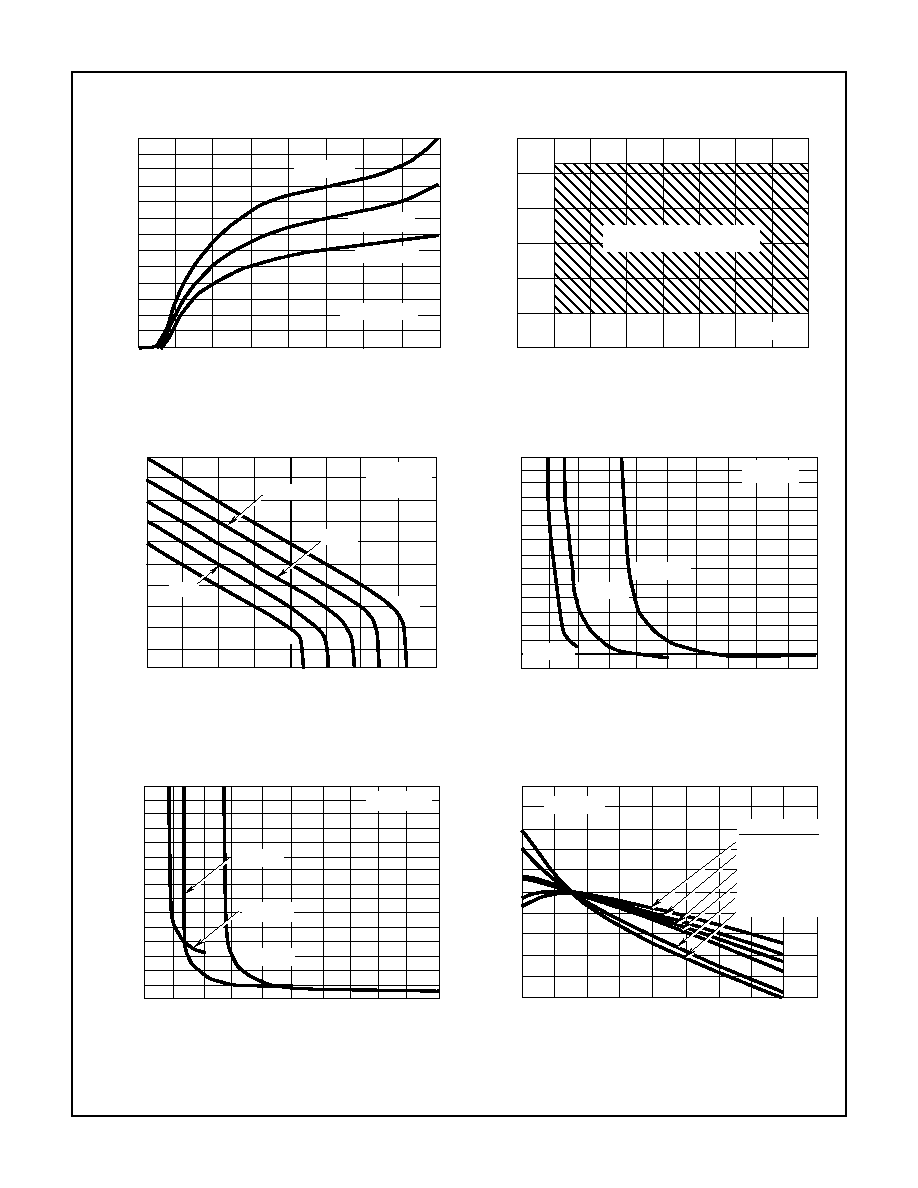
Typical Performance Curves
FIGURE 7. SUPPLY CURRENT vs SUPPLY VOLTAGE
FIGURE 8. RECOMMENDED RANGE OF TIMING COMPONENT
VALUES FOR ACCURATE TIMING
FIGURE 9. TIMEBASE FREE RUNNING FREQUENCY vs R AND C
FIGURE 10. MINIMUM TRIGGER PULSE WIDTH vs TRIGGER
AMPLITUDE
FIGURE 11. MINIMUM RESET PULSE WIDTH vs RESET
AMPLITUDE
FIGURE 12. NORMALIZED FREQUENCY STABILITY IN THE
ASTABLE MODE vs SUPPLY VOLTAGE
SUPPLY VOLTAGE (V)
0
2
4
6
8
10
12
14
16
0
260
240
220
200
180
160
140
120
100
80
60
40
20
SUPPL
Y CURRENT (
µ
A)
T
A
= -20
o
C
RESET MODE
T
A
= 25
o
C
T
A
= 75
o
C
TIMING CAPACITOR, C (
µ
F)
100pF
0.01
1
10
100
1000 10,000
100
100M
10M
1M
100k
10k
1k
TIMING RESIST
OR, R (
)
0.1
0.001
RECOMMENDED RANGE OF
TIMING COMPONENT VALUES
T
A
= 25
o
C
10M
TIME BASE FREQUENCY (Hz)
0.1
1
10
100
1K
10K
100K
1M
10M
10,000
µ
CAP
A
CIT
ANCE (F)
V
DD
= 5.0V
T
A
= 25
o
C
100k
10k
1k
1M
1,000
µ
100
µ
10
µ
1
µ
0.1
µ
0.01
µ
0.001
µ
100p
10p
1p
TRIGGER AMPLITUDE (V)
0
1
2
3
4
5
6
7
8
9
10
0
1500
1400
1300
1200
1100
1000
900
800
700
600
500
400
300
200
100
TRIGGER PULSE WIDTH (ns)
T
A
= 25
o
C
V
DD
= 5V
V
DD
= 2V
V
DD
= 16V
RESET AMPLITUDE (V)
0
1
2
3
4
5
6
7
8
9
10
0
1500
1400
1300
1200
1100
1000
900
800
700
600
500
400
300
200
100
RESET PULSE WIDTH (ns)
T
A
= 25
o
C
V
DD
= 5V
V
DD
= 2V
V
DD
= 16V
SUPPLY VOLTAGE (V)
2
10
12
14
16
18
20
+10.0
+8.0
+6.0
+4.0
+2.0
0.0
-2.0
-4.0
-6.0
-8.0
-10.0
NORMALIZED FREQ
UENCY DEVIA
TION (%)
T
A
= 25
o
C
R
8
6
4
C
10k
1M
1k
100k
10k
100k
0.001
µ
F
100pF
0.1
µ
F
0.001
µ
F
0.01
µ
F
0.01
µ
F
ICM7242

8-169
FIGURE 13. NORMALIZED FREQUENCY STABILITY IN THE
ASTABLE MODE vs TEMPERATURE
FIGURE 14. MAXIMUM DIVIDER FREQUENCY vs SUPPLY
VOLTAGE
FIGURE 15. DISCHARGE OUTPUT CURRENT vs DISCHARGE
OUTPUT VOLTAGE
FIGURE 16. OUTPUT SATURATION CURRENT vs OUTPUT
SATURATION VOLTAGE
Typical Performance Curves
(Continued)
TEMPERATURE (
o
C)
-25
0
25
50
75
+5
+4
+3
+2
+1
0
-1
-2
-3
-4
-5
NORMALIZED FREQ
UENCY DEVIA
TION (%)
5V
V
DD
15V
R = 10M
C = 0.1
µ
F
R = 1k
C = 0.1
µ
F
SUPPLY VOLTAGE (V)
2
10
12
14
16
18
20
100M
10M
1M
100K
10K
MAXIMUM DIVIDER FREQ
UENCY (Hz)
T
A
= 25
o
C
8
6
4
RC CONNECTED
TO GROUND
0
DISCHARGE SATURATION VOLTAGE (V)
0.01
0.1
1
10
0.1
100
10
1
DISCHARGE SINK CURRENT (mA)
T
A
= 25
o
C
V
DD
= 5V
V
DD
= 2V
V
DD
= 15V
OUTPUT SATURATION VOLTAGE (V)
0.01
0.1
1
10
0.1
100
10
1
OUTPUT SA
TURA
TION CURRENT (mA)
T
A
= 25
o
C
V
DD
= 5V
V
DD
= 2V
V
DD
= 15V
ICM7242