
9-23
August 1997
ICM7249
5
1
/
2
Digit LCD,
Micro-Power Event/Hour Meter
Features
∑ Hour Meter Requires Only 4 Parts Total
∑ Micropower Operation: < 1
µ
A at 2.8V (Typ)
∑ 10 Year Operation On One Lithium Cell. 2
1
/
2
Year
Battery Life with Display Connected
∑ Directly Drives 5
1
/
2
Digit LCD
∑ 14 Programmable Modes of Operation
∑ Times Hrs., 0.1 Hrs., 0.01 Hrs., 0.1 Mins.
∑ Counts 1's, 10's, 100's, 1000's
∑ Dual Function Input Circuit
- Selectable Debounce for Counter
- High-Pass Filter for Timer
∑ Direct AC Line Triggering with Input Resistor
∑ Winking "Timer Active" Display Output
∑ Display Test Feature
Applications
∑ AC or DC Hour Meters
∑ AC or DC Totalizers
∑ Portable Battery Powered Equipment
∑ Long Range Service Meters
Description
The ICM7249 Timer/Counter is intended for long-term
battery-supported industrial applications. The ICM7249
typically draws 1
µ
A during active timing or counting, due to
Intersil' special low-power design techniques. This allows
more than 10 years of continuous operation without battery
replacement. The chip offers four timing modes, eight
counting modes and four test modes.
The ICM7249 is a 48 lead device, powered by a single DC
voltage source and controlled by a 32.768kHz quartz crystal.
No other external components are required. Inputs to the
chip are TTL-compatible and outputs drive standard direct
drive LCD segments.
Pinout
ICM7249
(PDIP)
TOP VIEW
Ordering Information
PART NUMBER
TEMP.
RANGE (
o
C)
PACKAGE
PKG.
NO.
ICM7249IPM
-20 to 85
48 Ld PDIP
E48.6
C1
C0
GND
OSC OUTPUT
OSC INPUT
V
DD
BP
W
a1
b1
c1
d1
e1
g1
f1
a2
b2
c2
d2
e2
DT
S/S
C3
C2
48
47
46
45
17
5
6
7
8
9
10
11
12
13
14
15
16
18
19
20
21
22
23
24
d5
c5
b5
a5
f4
g4
e4
d4
c4
b4
a4
f3
g3
e3
d3
c3
b3
a3
f2
g2
32
44
43
42
41
40
39
38
37
36
35
34
33
31
30
29
28
27
26
25
1
2
3
4
b6/c6
f5
g5
e5
File Number
3170.1
CAUTION: These devices are sensitive to electrostatic discharge; follow proper IC Handling Procedures.
http://www.intersil.com or 407-727-9207
|
Copyright
©
Intersil Corporation 1999

9-24
Functional Block Diagram
S/S
V+
V-
B6
F5
G5
A1
W
BP
DT
OSC
2
15
DIVIDER
˜
6
˜
6
CONTR
OL
˜
10
˜
10
˜
10
˜
10
˜
10
˜
10
˜
10
˜
10
˜
2
1 SEG
VOLTAGE
C3
C2
C1
C0
DECODE
6 SEC
1Hz
32Hz
16
32Hz
OSC
IN
OSC
OUT
DEC
7 SEG
DEC
7 SEG
DEC
7 SEG
DEC
7 SEG
DEC
7 SEG
DEC
WINK
SEG
1Hz
DISPLAY
TEST
4
4
REGLATOR
SWITCH
DEBOUNCE
ICM7249

9-25
Absolute Maximum Ratings
Thermal Information
Supply Voltage (V
DD
- V
SS
) . . . . . . . . . . . . . . . . . . . . . . . . . . . . . 6V
Input Voltage, Pins 43 - 48 (Note 1) . . (V
SS
- 0.3V) to (V
DD
+ 0.3V)
Operating Conditions
Temperature Range . . . . . . . . . . . . . . . . . . . . . . . . . . -40
o
C to 85
o
C
Thermal Resistance (Typical, Note 2)
JA
(
o
C/W)
PDIP Package . . . . . . . . . . . . . . . . . . . . . . . . . . . . .
50
Maximum Junction Temperature . . . . . . . . . . . . . . . . . . . . . . . 150
o
C
Maximum Storage Temperature Range . . . . . . . . . .-65
o
C to 150
o
C
Maximum Lead Temperature (Soldering, 10s) . . . . . . . . . . . . 300
o
C
CAUTION: Stresses above those listed in "Absolute Maximum Ratings" may cause permanent damage to the device. This is a stress only rating and operation
of the device at these or any other conditions above those indicated in the operational sections of this specification is not implied.
NOTES:
1. Due to the SCR structure inherent in junction-isolated CMOS devices. the circuit can be put in a latchup mode it large currents are injected
into device inputs or outputs. For this reason special care should be taken in a system with multiple power supplies to prevent voltages
being applied to inputs or outputs before power is applied. If only inputs are affected, latchup also can be prevented by limiting the current
into the input terminal to less than 1mA.
2.
JA
is measured with the component mounted on an evaluation PC board in free air.
Electrical Specifications
Temperature = -40
o
C to 85
o
C, V
DD
= 2.5V to 5.5V, V
SS
= 0V, Unless Otherwise Specified. Typical
Specifications Measured at Temperature = 25
o
C and V
DD
= 2.8V, Unless Otherwise Specified
PARAMETER
TEST CONDITIONS
MIN
TYP
MAX
UNITS
Operating Voltage, V
DD
Note 1
2.5
-
5.5
V
Operating Current, I
DD
All Inputs = V
DD
or GND, Note 2
V
DD
= 2.8V
-
1.0
10.0
µ
A
V
DD
= 5.5V
-
4.0
20.0
µ
A
INPUT CURRENT
C0 - C3, I
IN
All Inputs V
DD
or GND
V
DD
= 2.8V
Note 3
0.0
-
1
µ
A
S/S, I
SS
0.5
1.5
3.0
µ
A
DT, I
DT
40.0
-
110
µ
A
INPUT VOLTAGE
C0 - C3, DT, S/S
V
IL
-
-
0.3V
DD
V
V
IH
0.7V
DD
-
-
V
Segment Output Voltage
V
OL
I
OL
= 1
µ
A
-
-
0.8
V
V
OH
I
OH
= 1
µ
A
V
DD
- 0.8
-
-
V
Backplane Output Voltage
V
OL
I
OL
= 10
µ
A
-
-
0.8
V
V
OH
I
OH
= 10
µ
A
V
DD
- 0.8
-
-
V
OSCILLATOR STABILITY
Temperature = 25
o
C, V
DD
= 2.5V to 5.5V
-
0.1
-
ppm
Temperature = -40
o
C to 85
o
C, V
DD
= 2.5V to 5.5V
-
5
-
ppm
S/S PULSE WIDTH
High-Pass Filter (Modes 0 - 3), t
HP
5
-
10,000
µ
s
Debounce (Modes 4, 6, 8, 10), t
DE
10,000
-
-
µ
s
Without Debounce (Modes 5, 7, 9, 11), t
DE
5
-
-
µ
s
NOTES:
1. Internal reset to 00000 requires a maximum V
DD
rise time of 1
µ
s. Longer rise times at power-up may cause improper reset.
2. Operating current is measured with the LCD disconnected, and input current I
SS
and I
DT
supplied externally.
3. Inputs C0 - C3 are latched internally and draw no DC current after switching. During switching, a 90
µ
A peak current may be drawn for 10ns.
ICM7249

9-26
Timing Waveforms
FIGURE 1. POWER ON/RESET WAVEFORMS
FIGURE 2. START/STOP INPUT HIGH-PASS FILTERING IN TIMING MODES
V
DD
OSC OUT
BP
ON
SEGMENTS
OFF
SEGMENTS
1
2
3
4
5
6
511
512
f
SEG
= 32Hz
t
r
f
BP
= 32Hz
f
0
= 32.768kHz
ONE
1
/
2
BACKPLANE CYCLE
POWER ON
RESET
40Hz < f < 50Hz
t
HP
TIMING ACTIVE DURING INTERVAL
S/S VALID
t
HP
S/S INVALID
S/S VALID
50Hz
f
120kHz
10ms < t
HP
< 12.5ms
5
µ
s
t
HP
10ms
t
HP
> 12.5ms
TIMING INTERMINATE DURING INTERVAL
TIMING ACTIVE DURING INTERVAL
ICM7249

9-27
FIGURE 3. WINK WAVEFORMS IN TIMING MODES
FIGURE 4. START/STOP INPUT DEBOUNCE FILTERING IN COUNTING MODES
FIGURE 5. WINK WAVEFORMS IN COUNTING MODES
Timing Waveforms
(Continued)
WINK GOES IN PHASE
WINK GOES OUT PHASE
16
17
1
BP
W
S/S
ON
SEGMENTS
OFF
SEGMENTS
TIMING ACTIVE
40Hz < f < 50Hz
t
DE
COUNT WITHOUT DEBOUNCE
ONE COUNT WITH DEBOUNCE
COUNT WITHOUT DEBOUNCE
UNKNOWN RESULTS WITH DEBOUNCE
COUNT WITH OR WITHOUT DEBOUNCE
S/S VALID
t
DE
S/S INVALID
S/S VALID
50Hz
f
120kHz
10ms < t
DE
< 12.5ms
5
µ
s
t
DE
10ms
t
DE
> 12.5ms
15
16
17
32
1
2
BP
WINK GOES IN PHASE
WINK GOES OUT PHASE
W
S/S
ICM7249

9-28
Pin Descriptions
FIGURE 6. DISPLAY TESTING
Timing Waveforms
(Continued)
14
15
16
17
64
1
2
BP
DT
ALL SEGMENTS
ON OR OFF
ALL SEGMENTS ON
ALL SEGMENTS OFF
DISPLAY RESTORED
PIN
NAME
DESCRIPTION
1
b6/c6
Half-Digit LCD Segment Output.
2
f5
Seven-Segment LCD Output.
3
g5
Seven-Segment LCD Output.
4
e5
Seven-Segment LCD Output.
5
d5
Seven-Segment LCD Output.
6
c5
Seven-Segment LCD Output.
7
b5
Seven-Segment LCD Output.
8
a5
Seven-Segment LCD Output.
9
f4
Seven-Segment LCD Output.
10
g4
Seven-Segment LCD Output.
11
e4
Seven-Segment LCD Output.
12
d4
Seven-Segment LCD Output.
13
c4
Seven-Segment LCD Output.
14
b4
Seven-Segment LCD Output.
15
a4
Seven-Segment LCD Output.
16
f3
Seven-Segment LCD Output.
17
g3
Seven-Segment LCD Output.
18
e3
Seven-Segment LCD Output.
19
d3
Seven-Segment LCD Output.
20
c3
Seven-Segment LCD Output.
21
b3
Seven-Segment LCD Output.
22
a3
Seven-Segment LCD Output.
23
f2
Seven-Segment LCD Output.
24
g2
Seven-Segment LCD Output.
25
e2
Seven-Segment LCD Output.
26
d2
Seven-Segment LCD Output.
27
c2
Seven-Segment LCD Output.
28
b2
Seven-Segment LCD Output.
29
a2
Seven-Segment LCD Output.
30
f1
Seven-Segment LCD Output.
31
91
Seven-Segment LCD Output.
32
e1
Seven-Segment LCD Output.
33
d1
Seven-Segment LCD Output.
34
c1
Seven-Segment LCD Output.
35
b1
Seven-Segment LCD Output.
36
a1
Seven-Segment LCD Output.
37
W
Wink-Segment Output.
38
BP
Backplane for LCD Reference.
39
V
DD
Positive Supply Voltage.
40
OSC IN
Quartz Crystal Connection.
41
OSC OUT
Quartz Crystal Connection.
42
GND
Supply GRouND.
43
C0
Mode-select Control Input.
44
C1
Mode-select Control Input.
45
C2
Mode-select Control Input.
46
C3
Mode-select Control Input.
47
S/S
Start/Stop Input.
48
DT
Display Test Input.
PIN
NAME
DESCRIPTION
ICM7249

9-29
Detailed Description
As the Functional Diagram shows the device consists of the
following building blocks:
∑ A 32.768kHz crystal oscillator with the associated dividers
to generate timebase signals for periods of 1s (frequency
of 1Hz), 6s (1/10 min) and 36s (1/100 hour), and 32Hz
signal for LCD drivers.
∑ A debounce/high-pass detect circuit for the S/S (Start/Stop)
input.
∑ A chain of cascaded decade counters, 3 decade counters
for prescaling and 5
1
/
2
BCD decade counters for display
driving.
∑ Display control circuitry and BCD to 7-segment decoder/
drivers.
∑ A control decoder to select different modes of operation.
This is done by routing different signals to the different
points in the chain of decade counters.
The control decoder has 4 inputs for selecting 16 possible
modes of operation, numbered 0 to 15. The 16 modes are
selected by placing the binary equivalent of the mode num-
ber on inputs C0 to C3. Table 2 shows the control inputs and
the modes of operation.
After applying power, the ICM7249 requires a rise time of t
r
to become active and for oscillation to begin, as shown in
Figure 1. The BP (backplane) output changes state once
every 512 cycles of the crystal oscillator, resulting in a
square wave of 32Hz. The display segments drive signal has
the same level and frequency as BP. Segments are off when
in phase with BP and are on when out of phase with BP.
A non-multiplexed LCD display is used because it is more
stable over temperature and allows many standard LCD
displays to be used.
Timer Mode of Operation
In modes 0 to 3 the device functions as an interval timer. In
this mode, one of the timebase signals will be routed to the
decade counters at a proper point in the chain. Depending
on the selected mode the display will be incremented at 0.1
min, 0.01 hour, 0.1 hour or 1 hour rates.
Control of timing function is handled by the S/S input. There
is a high-pass filtering effect on the S/S input in timer modes.
Referring to Figure 2, timing is active when either S/S is held
high for more than 12.5ms, or if input frequency is 50Hz to
120kHz. Driving S/S with a frequency between 40Hz to 50Hz
has an indeterminate effect on timing and should be
avoided. Note that the t
HP
intervals shown on Figure 1 are
also applied to the intervals when the S/S input is low.
Counter Mode of Operation
In modes 4 to 11 the device functions as an event counter or
totalizer. In this mode the S/S input will be routed to the decade
counters at a proper point in the chain. Each positive transition
of the S/S will be registered as one count. Depending on the
selected mode, the display will be incremented by each pulse,
every 10 pulses, every 100 pulses or every 1000 pulses.
In counter modes 4, 6, 8 and 10 the S/S input is subjected to
debounce filtering. Referring to Figure 4, only the pulses with
a frequency of less than 40Hz are valid and will be counted.
Input pulses with a frequency of 50Hz to 120kHz are not
counted individually, but each burst of input pulses will be
counted as one pulse if it lasts at least 12.5ms. Driving S/S
with a frequency between 40Hz to 50Hz has an indetermi-
nate result and should be avoided.
In counter modes 5, 7, 9 and 11 the S/S input is not
subjected to any debouncing action and input pulses will be
counted up to a frequency of 120kHz.
Wink Segment
The wink segment is provided as a annunciator to indicate the
ICM7249 is working. It can be connected to any kind of annun-
ciator on an LCD, like the flashing colons in a clock type LCD.
In the timer modes, the wink segment flashes while timing is
taking place. The wink segment waveform is shown on
Figure 3 for timer modes. On the positive transition of S/S,
the wink output turns off. It remains off for 16 BP cycles and
turns back on for another 16 cycles. If timing is still active,
this will be repeated, giving a wink flash rate of 1Hz; other-
wise, the wink segment remains on while timing is not active.
In the counter modes, the wink segment stays on until a
pulse occurs on S/S input, then it winks off indicating a pulse
is counted. This will happen regardless of whether the
display is incremented. Figure 5 shows the wink waveform
for counter modes. When a count occurs, the wink segment
TABLE 1. MODE SELECT TABLE
MODE
CONTROL PIN INPUTS
FUNCTION
C3
C2
C1
C0
0
0
0
0
0
1 Hour Interval Timer
1
0
0
0
1
0.1 Hour Interval Timer
2
0
0
1
0
0.01 Hour Interval Timer
3
0
0
1
1
0.1 Minute Interval Timer
4
0
1
0
0
1's Counter with Debounce
5
0
1
0
1
1's Counter
6
0
1
1
0
10's Counter with Debounce
7
0
1
1
1
10's Counter
8
1
0
0
0
100's Counter with Debounce
9
1
0
0
1
100's Counter
10
1
0
1
0
1000's Counter with Debounce
11
1
0
1
1
1000's counter
12
1
1
0
0
Test Display Digits
13
1
1
0
1
Internal Test
14
1
1
1
0
Internal Test
15
1
1
1
1
Reset
ICM7249

9-30
turns off at the end of the 16th BP cycle and turns back on at
the end of the 32nd BP cycle, giving a half-second wink. If
the counting occurs more frequently than once a second, the
wink output will continue to flash at the constant rate of 1Hz.
Display Test and Reset
The display may be tested at any time without disturbing
operation by pulsing DT high, as seen in Figure 6. On the
next positive transition of BP, all the segments turn on and
remain on until the end of the 16th BP cycle. This takes a
half-second or less. All the segments then turn off for an
additional 48 BP cycles (the end of the 64th cycle), after
which valid data returns to the display. As long as DT is held
high, the segments will remain on.
Additional display testing is provided by using mode 12. In this
mode each displayed decade is incremented on each positive
transition of S/S. Modes 13 and 14 are manufacturer testing only.
Mode 15 resets all the decades and internal counters to zero,
essentially bringing everything back to power-up status.
Applications
A typical use of the ICM7249 is seen in Figure 8, the Motor
Hour Meter. In this application the ICM7249 is configured as
an hours-in-use meter and shows how many whole hours of
line voltage have been applied. The resistor network and
high-pass filtering allow AC line activation of the S/S input.
This configuration, which is powered by a 3V lithium cell, will
operate continuously for 2
1
/
2
years. Without the display,
which only needs to be connected when a reading is
required, the span of operation is extended to 10 years.
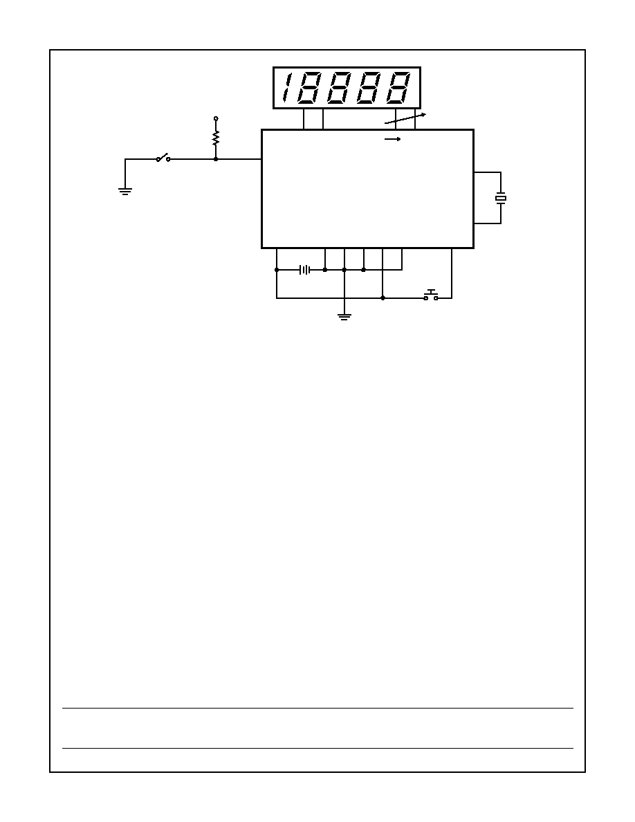
When the ICM7249 is configured as an attendance counter,
as shown in Figure 9, the display shows each increment. By
using mode 2, external debouncing of the gate switch is
unnecessary, provided the switch bounce is less than 10ms.
The 3V lithium battery can be replaced without disturbing
operation if a suitable capacitor is connected in parallel with
it. The display should be disconnected, if possible, during the
procedure to minimize current drain. The capacitor should
be large enough to store charge for the amount of time
needed to physically replace the battery (
t =
VC/I). A
100
µ
F capacitor initially charged to 3V will supply a current
of 1.0
µ
A for 50 seconds before its voltage drops to 2.5V,
which is the minimum operating voltage for the ICM7249.
Before the battery is removed, the capacitor should be
placed in parallel, across the V
DD
and GND terminals. After
the battery is replaced, the capacitor can be removed and
the display reconnected.
FIGURE 7. DIGITS SEGMENT ASSIGNMENT
a
b
c
d
f
g
e
FIGURE 8. MOTOR HOUR METER
120VAC
60Hz
36
W
BP
A1
B6/C6
OSC
1
OSC
0
DT
C3
C2
C1
C0
V
SS
V
DD
S/S
+3V L
i
AC MOTOR
10M
100K
10M
DISPLAY
TEST
32.768kHz
CRYSTAL
M
LCD
ICM7249
+
ICM7249
9-31
FIGURE 9. ATTENDANCE COUNTER
36
W
BP
A1
B6/C6
OSC
1
OSC
0
DT
C3
C2
C1
C0
V
SS
V
DD
S/S
+3V L
i
DISPLAY
TEST
32.768kHz
CRYSTAL
GATE
SWITCH
LCD
+3V TO +24V DC
20k
ICM7249
ICM7249
All Intersil semiconductor products are manufactured, assembled and tested under ISO9000 quality systems certification.
Intersil products are sold by description only. Intersil Corporation reserves the right to make changes in circuit design and/or specifications at any time without
notice. Accordingly, the reader is cautioned to verify that data sheets are current before placing orders. Information furnished by Intersil is believed to be accurate
and reliable. However, no responsibility is assumed by Intersil or its subsidiaries for its use; nor for any infringements of patents or other rights of third parties which
may result from its use. No license is granted by implication or otherwise under any patent or patent rights of Intersil or its subsidiaries.
For information regarding Intersil Corporation and its products, see web site http://www.intersil.com