 | –≠–ª–µ–∫—Ç—Ä–æ–Ω–Ω—ã–π –∫–æ–º–ø–æ–Ω–µ–Ω—Ç: IS80C88-2 | –°–∫–∞—á–∞—Ç—å:  PDF PDF  ZIP ZIP |

3-1
March 1997
80C88
CMOS 8/16-Bit Microprocessor
Features
∑ Compatible with NMOS 8088
∑ Direct Software Compatibility with 80C86, 8086, 8088
∑ 8-Bit Data Bus Interface; 16-Bit Internal Architecture
∑ Completely Static CMOS Design
- DC . . . . . . . . . . . . . . . . . . . . . . . . . . . . . 5MHz (80C88)
- DC . . . . . . . . . . . . . . . . . . . . . . . . . . . .8MHz (80C88-2)
∑ Low Power Operation
- ICCSB . . . . . . . . . . . . . . . . . . . . . . . . 500
µ
A Maximum
- ICCOP . . . . . . . . . . . . . . . . . . . . 10mA/MHz Maximum
∑ 1 Megabyte of Direct Memory Addressing Capability
∑ 24 Operand Addressing Modes
∑ Bit, Byte, Word, and Block Move Operations
∑ 8-Bit and 16-Bit Signed/Unsigned Arithmetic
∑ Bus-Hold Circuitry Eliminates Pull-up Resistors
∑ Wide Operating Temperature Ranges
- C80C88 . . . . . . . . . . . . . . . . . . . . . . . . . 0
o
C to + 70
o
C
- I80C88 . . . . . . . . . . . . . . . . . . . . . . . . . -40
o
C to +85
o
C
- M80C88 . . . . . . . . . . . . . . . . . . . . . . . -55
o
C to +125
o
C
Description
The Intersil 80C88 high performance 8/16-bit CMOS CPU is
manufactured using a self-aligned silicon gate CMOS pro-
cess (Scaled SAJI IV). Two modes of operation, MINimum
for small systems and MAXimum for larger applications such
as multiprocessing, allow user configuration to achieve the
highest performance level.
Full TTL compatibility (with the exception of CLOCK) and
industry-standard operation allow use of existing NMOS
8088 hardware and Intersil CMOS peripherals.
Complete software compatibility with the 80C86, 8086, and
8088 microprocessors allows use of existing software in new
designs.
Ordering Information
PACKAGE
TEMPERATURE RANGE
5MHz
8MHz
PKG. NO.
Plastic DIP
0
o
C to +70
o
C
CP80C88
CP80C88-2
E40.6
-40
o
C to +85
o
C
IP80C88
IP80C88-2
E40.6
PLCC
0
o
C to +70
o
C
CS80C88
CS80C88-2
N44.65
-40
o
C to +85
o
C
lS80C88
IS80C88-2
N44.65
CERDIP
0
o
C to +70
o
C
CD80C88
CD80C88-2
F40.6
-40
o
C to +85
o
C
ID80C88
ID80C88-2
F40.6
-55
o
C to +125
o
C
MD80C88/B
MD80C88-2/B
F40.6
SMD#
-55
o
C to +125
o
C
5962-8601601QA
-
F40.6
LCC
-55
o
C to +125
o
C
MR80C88/B
MR80C88-2/B
J44.A
SMD#
-55
o
C to +125
o
C
5962-8601601XA
-
J44.A
File Number
2949.1
[ /Title
(80C88
)
/Sub-
ject
(CMO
S 8/16-
Bit
Micro-
proces-
sor)
/Autho
r ()
/Key-
words
(Inter-
sil
Corpo-
ration,
8/16
Bit uP,
micro-
proces-
sor, 8
bit, 16
bit, 8-
bit, 16-
bit,
8088,
PC)
/Cre-
ator ()
CAUTION: These devices are sensitive to electrostatic discharge; follow proper IC Handling Procedures.
http://www.intersil.com or 407-727-9207
|
Copyright
©
Intersil Corporation 1999

3-2
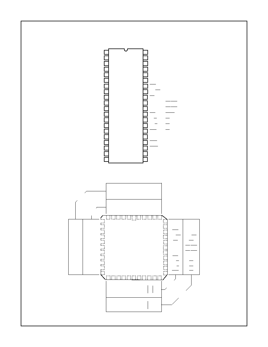
Pinouts
80C88 (DIP)
TOP VIEW
80C88 (PLCC/LCC)
TOP VIEW
13
1
2
3
4
5
6
7
8
9
10
11
12
14
15
16
17
18
19
20
GND
A14
A13
A12
A11
A10
A9
A8
AD7
AD6
AD5
AD4
AD3
AD2
AD1
AD0
NMI
INTR
CLK
GND
28
40
39
38
37
36
35
34
33
32
31
30
29
27
26
25
24
23
22
21
V
CC
A15
A16/S3
A17/S4
A18/S5
A19/S6
SS0
MN/MX
RD
(RQ/GT0)
(RQ/GT1)
(LOCK)
(S2)
(S1)
(S0)
(QS0)
(QS1)
TEST
READY
RESET
INTA
ALE
DEN
DT/R
IO/M
WR
HLDA
HOLD
MIN
MAX
(HIGH)
MODE
MODE
14
13
12
11
10
9
8
7
17
16
15
2
5
30
35
39
38
37
36
33
34
32
31
29
4
6
3
1
40
41
42
43
44
28
27
26
25
24
23
22
21
20
19
18
A19/S6
SS0
MN/MX
RD
HOLD
HLDA
WR
IO/M
DT/R
DEN
NC
NC
A19/S6
(HIGH)
MN/MX
RD
RQ/GT0
RQ/GT1
LOCK
S2
S1
S0
A9
A8
AD7
AD6
AD5
AD4
AD3
AD2
AD1
AD0
A10
A10
A9
A8
AD7
AD6
AD5
AD4
AD3
AD2
AD1
AD0
A12
A13
A14
GND
NC
V
CC
A15
A16/S3
A17/S4
A18/S5
A11
A11
A12
A13
A14
GND
NC
V
CC
A15
A16/S3
A17/S4
A18/S5
NMI
INTR
CLK
GND
NC
RESET
READ
Y
TEST
QS1
QS0
NC
NC
NMI
INTR
CLK
GND
NC
RESET
READ
Y
TEST
INT
A
ALE
MAX MODE
80C88
MIN MODE
80C88
MAX MODE
80C88
MIN MODE
80C88
80C88

3-3
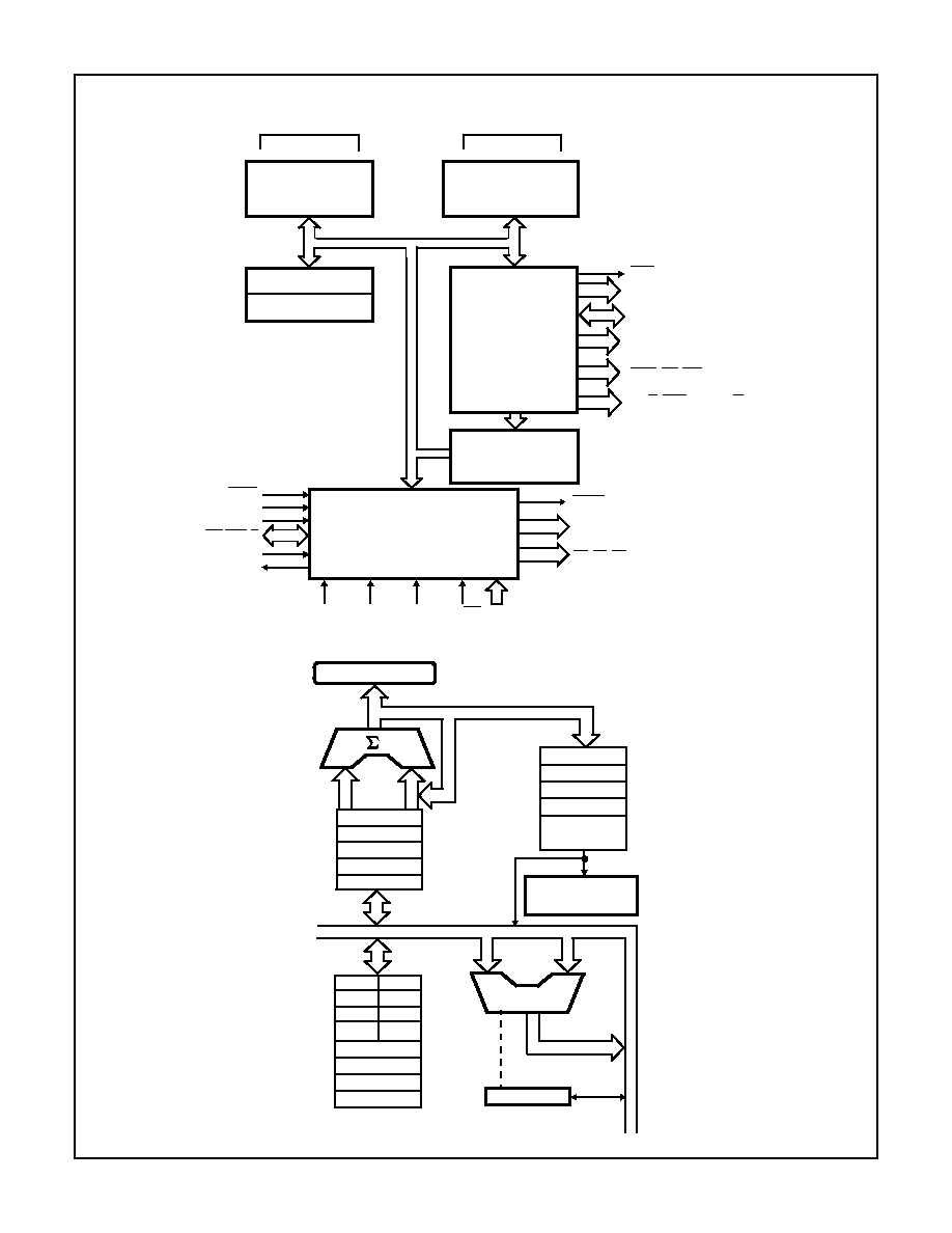
Functional Diagram
REGISTER FILE
EXECUTION UNIT
CONTROL AND TIMING
INSTRUCTION
QUEUE
4-BYTE
FLAGS
16-BIT ALU
BUS
8
4
QS0, QS1
S2, S1, S0
2
4
3
GND
V
CC
CLK
RESET READY
BUS INTERFACE UNIT
RELOCATION
REGISTER FILE
3
A19/S6. . . A16/S3
INTA, RD, WR
DT/R, DEN, ALE, IO/M
SSO/HIGH
2
SEGMENT REGISTERS
AND
INSTRUCTION POINTER
(5 WORDS)
DATA POINTER
AND
INDEX REGS
(8 WORDS)
TEST
INTR
NMI
HLDA
HOLD
RQ/GT0, 1
LOCK
MN/MX
3
ES
CS
SS
DS
IP
AH
BH
CH
DH
AL
BL
CL
DL
SP
BP
SI
DI
ARITHMETIC/
LOGIC UNIT
B-BUS
C-BUS
EXECUTION
UNIT
INTERFACE
UNIT
BUS
QUEUE
INSTRUCTION
STREAM BYTE
EXECUTION UNIT
CONTROL SYSTEM
FLAGS
MEMORY INTERFACE
A-BUS
AD7-AD0
8
A8-A15
INTERFACE
UNIT
80C88

3-4
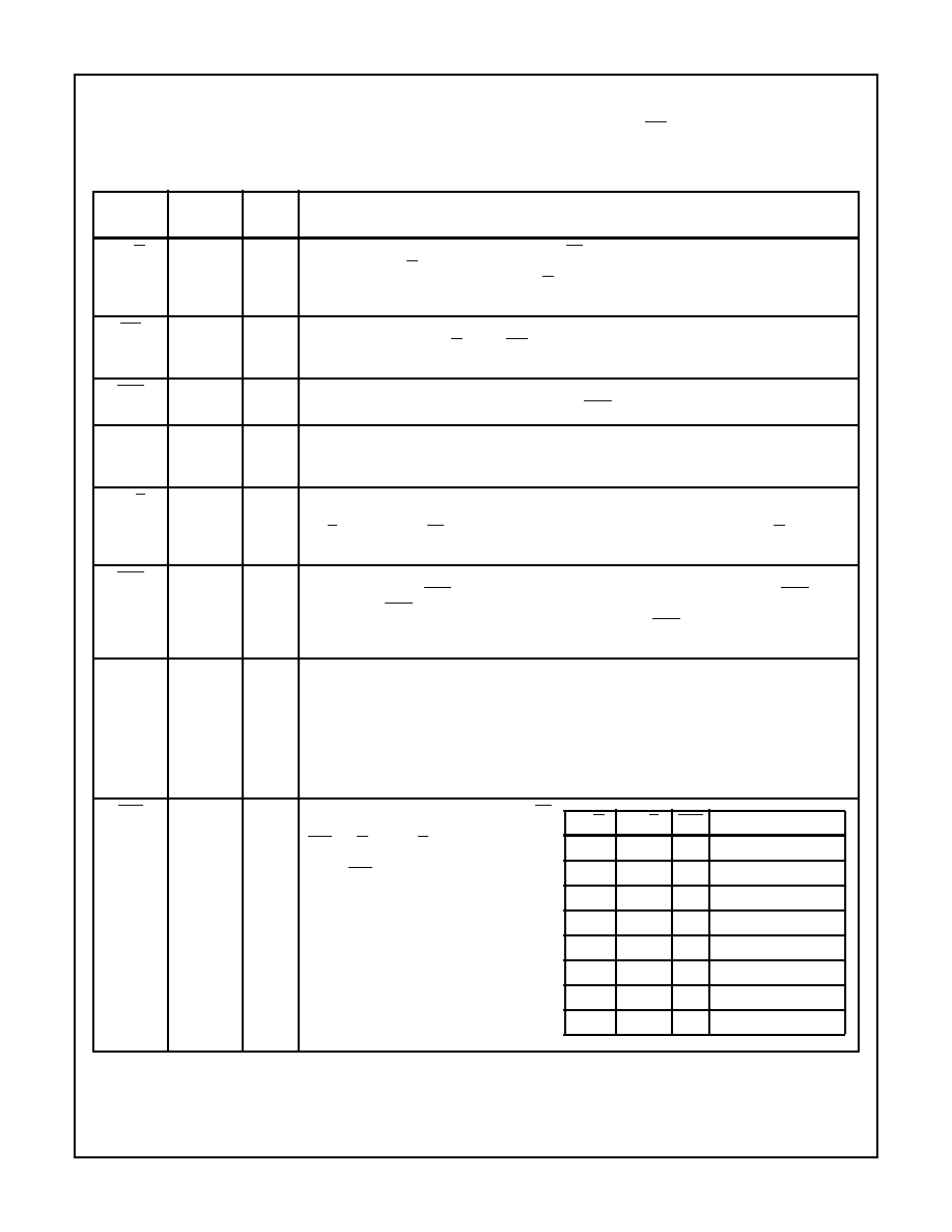
Pin Description
The following pin function descriptions are for 80C88 systems in either minimum or maximum mode. The "local bus" in these
descriptions is the direct multiplexed bus interface connection to the 80C88 (without regard to additional bus buffers).
SYMBOL
PIN
NUMBER
TYPE
DESCRIPTION
AD7-AD0
9-16
I/O
ADDRESS DATA BUS: These lines constitute the time multiplexed memory/IO address (T1) and
data (T2,T3,Tw and T4) bus. These lines are active HIGH and are held at high impedance to the last
valid level during interrupt acknowledge and local bus "hold acknowledge" or "grant sequence"
A15-A8
2-8, 39
O
ADDRESS BUS: These lines provide address bits 8 through 15 for the entire bus cycle (T1-T4).
These lines do not have to be latched by ALE to remain valid. A15-A8 are active HIGH and are held
at high impedance to the last valid logic level during interrupt acknowledge and local bus "hold
acknowledge" or "grant sequence".
A19/S6,
A18/S5,
A17/S4,
A16/S3
35
36
37
38
O
O
O
O
ADDRESS/STATUS: During T1, these are the four most
significant address lines for memory operations. During
I/O operations, these lines are LOW. During memory and
I/O operations, status information is available on these
lines during T2, T3, TW and T4. S6 is always LOW. The
status of the interrupt enable flag bit (S5) is updated at the
beginning of each clock cycle. S4 and S3 are encoded as
shown.
This information indicates which segment register is
presently being used for data accessing.
These lines are held at high impedance to the last valid
logic level during local bus "hold acknowledge" or "grant
Sequence".
RD
32
O
READ: Read strobe indicates that the processor is performing a memory or I/O read cycle, depend-
ing on the state of the IO/M pin or S2. This signal is used to read devices which reside on the 80C88
local bus. RD is active LOW during T2, T3, Tw of any read cycle, and is guaranteed to remain HIGH
in T2 until the 80C88 local bus has floated.
This line is held at a high impedance logic one state during "hold acknowledge" or "grant sequence".
READY
22
I
READY: is the acknowledgment from the address memory or I/O device that it will complete the data
transfer. The RDY signal from memory or I/O is synchronized by the 82C84A clock generator to from
READY. This signal is active HIGH. The 80C88 READY input is not synchronized. Correct operation
is not guaranteed if the set up and hold times are not met.
INTR
18
I
INTERRUPT REQUEST: is a level triggered input which is sampled during the last clock cycle of
each instruction to determine if the processor should enter into an interrupt acknowledge operation.
A subroutine is vectored to via an interrupt vector lookup table located in system memory. It can be
internally masked by software resetting the interrupt enable bit. INTR is internally synchronized. This
signal is active HIGH.
TEST
23
I
TEST: input is examined by the "wait for test" instruction. If the TEST input is LOW, execution con-
tinues, otherwise the processor waits in an "idle" state. This input is synchronized internally during
each clock cycle on the leading edge of CLK.
NMI
17
I
NONMASKABLE INTERRUPT: is an edge triggered input which causes a type 2 interrupt. A sub-
routine is vectored to via an interrupt vector lookup table located in system memory. NMI is not
maskable internally by software. A transition from a LOW to HIGH initiates the interrupt at the end
of the current instruction. This input is internally synchronized.
RESET
21
I
RESET: cases the processor to immediately terminate its present activity. The signal must transition
LOW to HIGH and remain active HIGH for at least four clock cycles. It restarts execution, as de-
scribed in the instruction set description, when RESET returns LOW. RESET is internally synchro-
nized.
CLK
19
I
CLOCK: provides the basic timing for the processor and bus controller. It is asymmetric with a 33%
duty cycle to provide optimized internal timing.
V
CC
40
V
CC
: is the +5V power supply pin. A 0.1
µ
F capacitor between pins 20 and 40 recommended for de-
coupling.
GND
1, 20
GND: are the ground pins (both pins must be connected to system ground). A 0.1
µ
F capacitor be-
tween pins 1 and 20 is recommended for decoupling.
MN/MX
33`
I
MINIMUM/MAXIMUM: indicates the mode in which the processor is to operate. The two modes are
discussed in the following sections.
S4
S3
CHARACTERISTICS
0
0
Alternate Data
0
1
Stack
1
0
Code or None
1
1
Data
80C88

3-5
Pin Description
(Continued)
The following pin function descriptions are for 80C88 system in minimum mode (i.e., MN/MX = V
CC
). Only the pin functions
which are unique to the minimum mode are described; all other pin functions are as described above.
MINIMUM MODE SYSTEM
SYMBOL
PIN
NUMBER
TYPE
DESCRIPTION
IO/M
28
O
STATUS LINE: is an inverted maximum mode S2. It is used to distinguish a memory access from
an I/O access. IO/M becomes valid in the T4 preceding a bus cycle and remains valid until the final
T4 of the cycle (I/O = HIGH, M = LOW). IO/M is held to a high impedance logic one during local bus
"hold acknowledge".
WR
29
O
Write: strobe indicates that the processor is performing a write memory or write I/O cycle, depend-
ing on the state of the IO/M signal. WR is active for T2, T3, and Tw of any write cycle. It is active
LOW, and is held to high impedance logic one during local bus "hold acknowledge".
INTA
24
O
INTA: is used as a read strobe for interrupt acknowledge cycles. It is active LOW during T2, T3 and
Tw of each interrupt acknowledge cycle. Note that INTA is never floated.
ALE
25
O
ADDRESS LATCH ENABLE: is provided by the processor to latch the address into the
82C82/82C83 address latch. It is a HIGH pulse active during clock low of T1 of any bus cycle. Note
that ALE is never floated.
DT/R
27
O
DATA TRANSMIT/RECEIVE: is needed in a minimum system that desires to use an 82C86/82C87
data bus transceiver. It is used to control the direction of data flow through the transceiver. Logically,
DT/R is equivalent to S1 in the maximum mode, and its timing is the same as for IO/M (T = HIGH,
R = LOW). This signal is held to a high impedance logic one during local bus "hold acknowledge".
DEN
26
O
DATA ENABLE: is provided as an output enable for the 82C86/82C87 in a minimum system which
uses the transceiver. DEN is active LOW during each memory and I/O access, and for INTA cycles.
For a read or INTA cycle, it is active from the middle of T2 until the middle of T4, while for a write
cycle, it is active from the beginning of T2 until the middle of T4. DEN is held to high impedance logic
one during local bus "hold acknowledge".
HOLD,
HLDA
31
30
I
O
HOLD: indicates that another master is requesting a local bus "hold". To be acknowledged, HOLD
must be active HIGH. The processor receiving the "hold" request will issue HLDA (HIGH) as an
acknowledgment, in the middle of a T4 or T1 clock cycle. Simultaneous with the issuance of HLDA
the processor will float the local bus and control lines. After HOLD is detected as being LOW, the
processor lowers HLDA, and when the processor needs to run another cycle, it will again drive the
local bus and control lines.
Hold is not an asynchronous input. External synchronization should be provided if the system cannot
otherwise guarantee the set up time.
SS0
34
O
STATUS LINE: is logically equivalent to S0
in the maximum mode. The combination of
SS0, IO/M and DT/R allows the system to
completely decode the current bus cycle
status. SS0 is held to high impedance logic
one during local bus "hold acknowledge".
IO/M
DT/R
SS0
CHARACTERISTICS
1
0
0
Interrupt Acknowledge
1
0
1
Read I/O Port
1
1
0
Write I/O Port
1
1
1
Halt
0
0
0
Code Access
0
0
1
Read Memory
0
1
0
Write Memory
0
1
1
Passive
80C88

