Äîêóìåíòàöèÿ è îïèñàíèÿ www.docs.chipfind.ru
4-1
F o r m e r l y F R L 4 3 0 R 4
JANSR2N7281
Radiation Hardened, N-Channel
Power MOSFET
The Intersil has designed a series of SECOND
GENERATION hardened power MOSFETs of both N-
Channel and P-Channel enhancement types with ratings
from 100V to 500V, 1A to 60A, and on resistance as low as
25m
. Total dose hardness is offered at 100K RAD (Si) and
1000K RAD (Si) with neutron hardness ranging from 1E13
for 500V product to 1E14 for 100V product. Dose rate
hardness (GAMMA DOT) exists for rates to 1E9 without
current limiting and 2E12 with current limiting.
This MOSFET is an enhancement-mode silicon-gate power
field effect transistor of the vertical DMOS (VDMOS)
structure. It is specially designed and processed to exhibit
minimal characteristic changes to total dose (GAMMA) and
neutron (n
o
) exposures. Design and processing efforts are
also directed to enhance survival to dose rate (GAMMA
DOT) exposure.
Also available at other radiation and screening levels. See us
on the web, Intersil' home page: www.semi.intersil.com.
Contact your local Intersil Sales Office for additional
information.
Die family TA17635.
MIL-PRF-19500/604.
Features
· 2A, 500V, r
DS(ON)
= 2.50
· Total Dose
- Meets Pre-RAD Specifications to 100K RAD (Si)
· Dose Rate
- Typically Survives 3E9 RAD (Si)/s at 80% BV
DSS
- Typically Survives 2E12 if Current Limited to I
DM
· Photo Current
- 8nA Per-RAD (Si)/s Typically
· Neutron
- Maintain Pre-RAD Specifications for 3E12
Neutrons/cm
2
- Usable to 3E13 Neutrons/cm
2
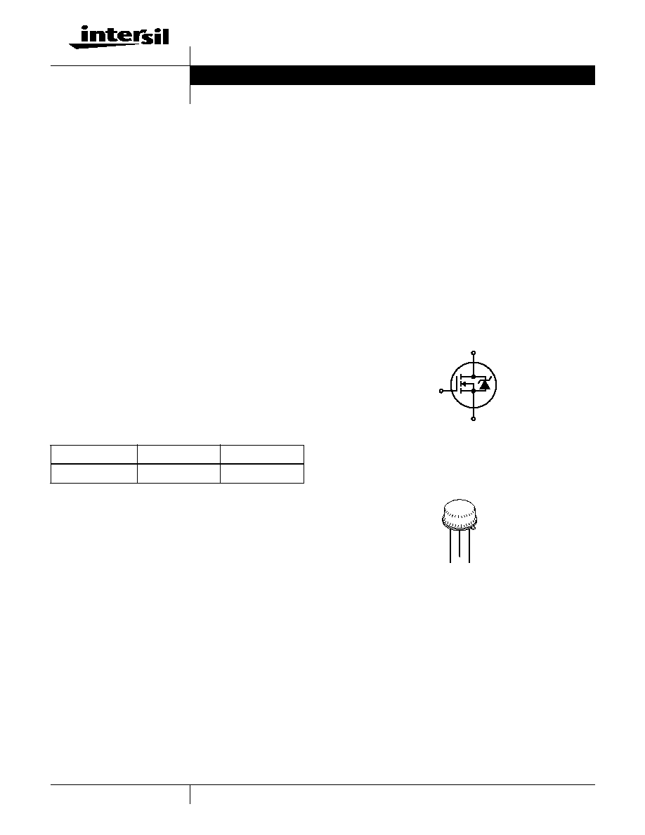
Symbol
Package
TO-205AF
Ordering Information
PART NUMBER
PACKAGE
BRAND
JANSR2N7281
TO-205AF
JANSR2N7281
D
G
S
S
G
D
Data Sheet
November 1998
File Number
4294
CAUTION: These devices are sensitive to electrostatic discharge; follow proper IC Handling Procedures.
www.intersil.com or 407-727-9207
|
Copyright
©
Intersil Corporation 1999
4-2
Absolute Maximum Ratings
T
C
= 25
o
C, Unless Otherwise Specified
JANSR2N7281
UNITS
Drain to Source Voltage . . . . . . . . . . . . . . . . . . . . . . . . . . . . . . . . . . . . . . . . . . . . . . . . . . . . . V
DS
500
V
Drain to Gate Voltage (R
GS
= 20k
) . . . . . . . . . . . . . . . . . . . . . . . . . . . . . . . . . . . . . . . . . .V
DGR
500
V
Continuous Drain Current
T
C
= 25
o
C . . . . . . . . . . . . . . . . . . . . . . . . . . . . . . . . . . . . . . . . . . . . . . . . . . . . . . . . . . . . . . .I
D
2
A
T
C
= 100
o
C . . . . . . . . . . . . . . . . . . . . . . . . . . . . . . . . . . . . . . . . . . . . . . . . . . . . . . . . . . . . . .I
D
1
A
Pulsed Drain Current . . . . . . . . . . . . . . . . . . . . . . . . . . . . . . . . . . . . . . . . . . . . . . . . . . . . . . . I
DM
6
A
Gate to Source Voltage . . . . . . . . . . . . . . . . . . . . . . . . . . . . . . . . . . . . . . . . . . . . . . . . . . . . . V
GS
±
20
V
Maximum Power Dissipation
T
C
= 25
o
C . . . . . . . . . . . . . . . . . . . . . . . . . . . . . . . . . . . . . . . . . . . . . . . . . . . . . . . . . . . . . . P
T
25
W
T
C
= 100
o
C . . . . . . . . . . . . . . . . . . . . . . . . . . . . . . . . . . . . . . . . . . . . . . . . . . . . . . . . . . . . . P
T
10
W
Linear Derating Factor . . . . . . . . . . . . . . . . . . . . . . . . . . . . . . . . . . . . . . . . . . . . . . . . . . . . . . .
0.20
W/
o
C
Single Pulsed Avalanche Current, L = 100
µ
H, (See Test Figure) . . . . . . . . . . . . . . . . . . . . . . I
AS
6
A
Continuous Source Current (Body Diode) . . . . . . . . . . . . . . . . . . . . . . . . . . . . . . . . . . . . . . . . . I
S
2
A
Pulsed Source Current (Body Diode). . . . . . . . . . . . . . . . . . . . . . . . . . . . . . . . . . . . . . . . . . . I
SM
6
A
Operating and Storage Temperature . . . . . . . . . . . . . . . . . . . . . . . . . . . . . . . . . . . . . . T
JC
, T
STG
-55 to 150
o
C
Lead Temperature (During Soldering) . . . . . . . . . . . . . . . . . . . . . . . . . . . . . . . . . . . . . . . . . . . T
L
(Distance >0.063in (1.6mm) from Case, 10s Max)
300
o
C
Weight (Typical) . . . . . . . . . . . . . . . . . . . . . . . . . . . . . . . . . . . . . . . . . . . . . . . . . . . . . . . . . . . . . .
1.0
g
CAUTION: Stresses above those listed in "Absolute Maximum Ratings" may cause permanent damage to the device. This is a stress only rating and operation of the
device at these or any other conditions above those indicated in the operational sections of this specification is not implied.
Electrical Specifications
T
C
= 25
o
C, Unless Otherwise Specified
PARAMETER
SYMBOL
TEST CONDITIONS
MIN
TYP
MAX
UNITS
Drain to Source Breakdown Voltage
BV
DSS
I
D
= 1mA, V
GS
= 0V
500
-
-
V
Gate Threshold Voltage
V
GS(TH)
V
GS
= V
DS
,
I
D
= 1mA
T
C
= -55
o
C
-
-
5.0
V
T
C
= 25
o
C
2.0
-
4.0
V
T
C
= 125
o
C
1.0
-
-
V
Zero Gate Voltage Drain Current
I
DSS
V
DS
= 400V,
V
GS
= 0V
T
C
= 25
o
C
-
-
25
µ
A
T
C
= 125
o
C
-
-
250
µ
A
Gate to Source Leakage Current
I
GSS
V
GS
=
±
20V
T
C
= 25
o
C
-
-
100
nA
T
C
= 125
o
C
200
nA
Drain to Source On-State Voltage
V
DS(ON)
V
GS
= 10V, I
D
= 2A
5.25
V
On Resistance
r
DS(ON)
I
D
= 1A,
V
GS
= 10V
T
C
= 25
o
C
-
-
2.50
T
C
= 125
o
C
-
-
6.50
Turn-On Delay Time
t
d(ON)
V
DD
= 250V, I
D
= 2A,
R
L
= 125
, V
GS
= 10V,
R
GS
=25
-
-
46
ns
Rise Time
t
r
-
-
58
ns
Turn-Off Delay Time
t
d(OFF)
-
-
208
ns
Fall Time
t
f
-
-
54
ns
Total Gate Charge
Q
g(TOT)
V
GS
= 0V to 20V
V
DD
= 250V,
I
D
= 2A,
R
L
= 125
-
-
130
nC
Gate Charge at 10V
Q
g(10)
V
GS
= 0V to 10V
-
-
64
nC
Threshold Gate Charge
Q
g(TH)
V
GS
= 0V to 2V
-
-
4
nC
Gate Charge Source
Q
gs
-
-
12
nC
Gate Charge Drain
Q
gd
-
-
32
nC
Thermal Resistance Junction to Case
R
JC
-
-
5.0
o
C/W
Thermal Resistance Junction to Ambient
R
JA
-
-
175
o
C/W
Source to Drain Diode Specifications
PARAMETER
SYMBOL
TEST CONDITIONS
MIN
TYP
MAX
UNITS
Forward Voltage
V
SD
I
SD
= 2A
0.6
-
1.8
V
Reverse Recovery Time
t
rr
I
SD
= 2A, dI
SD
/dt = 100A/
µ
s
-
-
900
ns
JANSR2N7281
4-3
Electrical Specifications up to 100K RAD
T
C
= 25
o
C, Unless Otherwise Specified
PARAMETER
SYMBOL
TEST CONDITIONS
MIN
MAX
UNITS
Drain to Source Breakdown Volts
(Note 3)
BV
DSS
V
GS
= 0, I
D
= 1mA
500
-
V
Gate to Source Threshold Volts
(Note 3)
V
GS(TH)
V
GS
= V
DS
, I
D
= 1mA
2.0
4.0
V
Gate to Body Leakage
(Notes 2, 3)
I
GSS
V
GS
=
±
20V, V
DS
= 0V
-
100
nA
Zero-Gate Leakage
(Note 3)
I
DSS
V
GS
= 0, V
DS
= 400V
-
25
µ
A
Drain to Source On-State Volts
(Notes 1, 3)
V
DS(ON)
V
GS
= 10V, I
D
= 2A
-
5.25
V
Drain to Source On Resistance
(Notes 1, 3)
r
DS(ON)
V
GS
= 10V, I
D
= 1A
-
2.5
NOTES:
1. Pulse test, 300
µ
s Max.
2. Absolute value.
3. Insitu Gamma bias must be sampled for both V
GS
= 10V, V
DS
= 0V and V
GS
= 0V, V
DS
= 80% BV
DSS
.
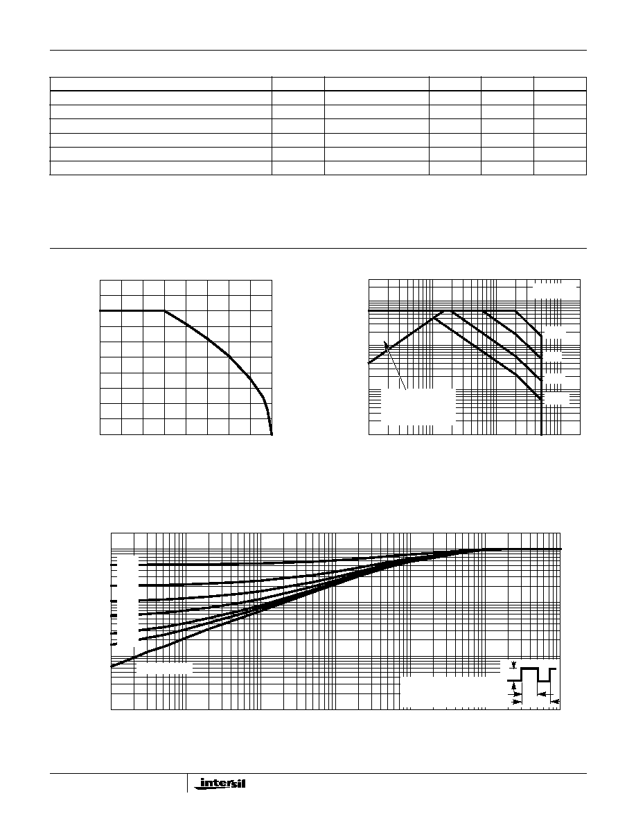
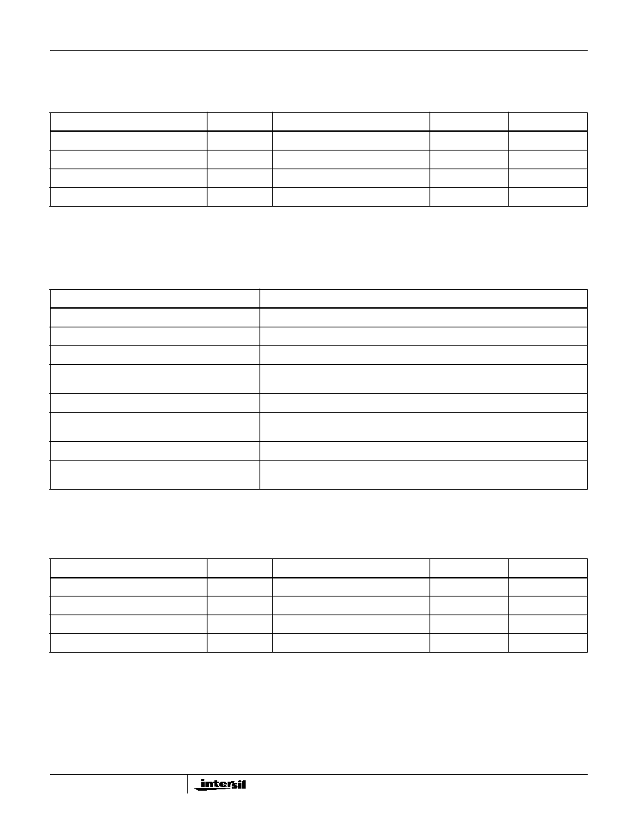
Typical Performance Curves
Unless Otherwise Specified
FIGURE 1. MAXIMUM CONTINUOUS DRAIN CURRENT vs
CASE TEMPERATURE
FIGURE 2. FORWARD BIAS SAFE OPERATING AREA
FIGURE 3. NORMALIZED MAXIMUM TRANSIENT THERMAL RESPONSE
I
D
, DRAIN (A)
T
C
, CASE TEMPERATURE (
o
C)
150
100
50
0
-50
0
2
1
10
1
1
0.1
I
D
,
DRAIN CURRENT (A)
V
DS
, DRAIN TO SOURCE VOLTAGE (V)
10
0.01
1000
30
100
OPERATION IN THIS
AREA MAY BE
LIMITED BY r
DS(ON)
100
µ
s
1ms
10ms
100ms
T
C
= 25
o
C
NORMALIZED
THERMAL RESPONSE (Z
qJC
)
t, RECTANGULAR PULSE DURATION (s)
10
-5
10
-4
10
-3
10
-2
10
-1
10
0
10
1
0.001
0.01
0.1
P
DM
t
1
t
2
NOTES:
DUTY FACTOR: D = t
1
/t
2
PEAK T
J
= P
DM
x Z
qJC
+ T
C
SINGLE PULSE
0.01
0.02
0.2
0.1
0.05
0.5
1.0
JANSR2N7281
4-4
Test Circuits and Waveforms
FIGURE 4. UNCLAMPED ENERGY TEST CIRCUIT
FIGURE 5. UNCLAMPED ENERGY WAVEFORMS
FIGURE 6. RESISTIVE SWITCHING TEST CIRCUIT
FIGURE 7. RESISTIVE SWITCHING WAVEFORMS
FIGURE 8. BASIC GATE CHARGE WAVEFORM
t
P
V
GS
20V
L
+
-
V
DS
V
DD
DUT
VARY t
P
TO OBTAIN
REQUIRED PEAK I
AS
0V
50
50
50V-150V
I
AS
+
-
ELECTRONIC SWITCH OPENS
WHEN I
AS
IS REACHED
CURRENT
TRANSFORMER
V
DD
V
DS
BV
DSS
t
P
I
AS
t
AV
V
DS
DUT
R
GS
0V
V
GS
= 10V
V
DD
R
L
t
d(ON)
t
r
90%
10%
V
DS
90%
10%
t
f
t
d(OFF)
t
OFF
90%
50%
50%
10%
PULSE WIDTH
V
GS
t
ON
CHARGE
Q
GD
Q
G
V
G
Q
GS
BASIC GATE CHARGE WAVEFORM
10V
JANSR2N7281
4-5
Screening Information
Screening is performed in accordance with the latest revision in effect of MIL-S-19500, (Screening Information Table).
Delta Tests and Limits (JANS)
T
C
= 25
o
C, Unless Otherwise Specified
PARAMETER
SYMBOL
TEST CONDITIONS
MAX
UNITS
Gate to Source Leakage Current
I
GSS
V
GS
=
±
20V
±
20 (Note 4)
nA
Zero Gate Voltage Drain Current
I
DSS
V
DS
= 80% Rated Value
±
25 (Note 4)
µ
A
On Resistance
r
DS(ON)
T
C
= 125
o
C at Rated I
D
±
20% (Note 5)
Gate Threshold Voltage
V
GS(TH)
I
D
= 1.0mA
±
20% (Note 5)
V
NOTES:
4. Or 100% of Initial Reading (whichever is greater).
5. Of Initial Reading.
Screening Information
TEST
JANS
Gate Stress
V
GS
= 30V, t = 250
µ
s
Pind
Required
Pre Burn-In Tests (Note 6)
MIL-S-19500 Group A, Subgroup 2 (All Static Tests at 25
o
C)
Steady State Gate Bias (Gate Stress)
MIL-STD-750, Method 1042, Condition B
V
GS
= 80% of Rated Value, T
A
= 150
o
C, Time = 48 hours
Interim Electrical Tests (Note 6)
All Delta Parameters Listed in the Delta Tests and Limits Table
Steady State Reverse Bias (Drain Stress)
MIL-STD-750, Method 1042, Condition A
V
DS
= 80% of Rated Value, T
A
= 150
o
C, Time = 240 hours
PDA
5%
Final Electrical Tests (Note 6)
MIL-S-19500, Group A,
Subgroups 2 and 3
NOTE:
6. Test limits are identical pre and post burn-in.
Additional Screening Tests
PARAMETER
SYMBOL
TEST CONDITIONS
MAX
UNITS
Safe Operating Area
SOA
V
DS
= 200V, t = 10ms
0.50
A
Unclamped Inductive Switching
I
AS
V
GS(PEAK)
= 15V, L = 0.1mH
6
A
Thermal Response
V
SD
t
H
= 10ms; V
H
= 25V; I
H
= 2A
92
mV
Thermal Impedance
V
SD
t
H
= 500ms; V
H
= 25V; I
H
= 1A
190
mV
JANSR2N7281

4-6
Rad Hard Data Packages - Intersil Power Transistors
1. JANS Rad Hard - Standard Data Package
A. Certificate of Compliance
B. Serialization Records
C. Assembly Flow Chart
D. SEM Photos and Report
E. Preconditioning - Attributes Data Sheet
- Hi-Rel Lot Traveler
- HTRB - Hi Temp Gate Stress Post
Reverse Bias Data and Delta Data
- HTRB - Hi Temp Drain Stress Post
Reverse Bias Delta Data
F. Group A
- Attributes Data Sheet
G. Group B
- Attributes Data Sheet
H. Group C
- Attributes Data Sheet
I. Group D
- Attributes Data Sheet
2. JANS Rad Hard - Optional Data Package
A. Certificate of Compliance
B. Serialization Records
C. Assembly Flow Chart
D. SEM Photos and Report
E. Preconditioning - Attributes Data Sheet
- Hi-Rel Lot Traveler
- HTRB - Hi Temp Gate Stress Post
Reverse Bias Data and Delta Data
- HTRB - Hi Temp Drain Stress Post
Reverse Bias Delta Data
- X-Ray and X-Ray Report
F. Group A
- Attributes Data Sheet
- Hi-Rel Lot Traveler
- Subgroups A2, A3, A4, A5 and A7 Data
G. Group B
- Attributes Data Sheet
- Hi-Rel Lot Traveler
- Subgroups B1, B3, B4, B5 and B6 Data
H. Group C
- Attributes Data Sheet
- Hi-Rel Lot Traveler
- Subgroups C1, C2, C3 and C6 Data
I. Group D
- Attributes Data Sheet
- Hi-Rel Lot Traveler
- Pre and Post Radiation Data
JANSR2N7281
4-7
All Intersil semiconductor products are manufactured, assembled and tested under ISO9000 quality systems certification.
Intersil semiconductor products are sold by description only. Intersil Corporation reserves the right to make changes in circuit design and/or specifications at any time with-
out notice. Accordingly, the reader is cautioned to verify that data sheets are current before placing orders. Information furnished by Intersil is believed to be accurate and
reliable. However, no responsibility is assumed by Intersil or its subsidiaries for its use; nor for any infringements of patents or other rights of third parties which may result
from its use. No license is granted by implication or otherwise under any patent or patent rights of Intersil or its subsidiaries.
For information regarding Intersil Corporation and its products, see web site www.intersil.com
Sales Office Headquarters
NORTH AMERICA
Intersil Corporation
P. O. Box 883, Mail Stop 53-204
Melbourne, FL 32902
TEL: (407) 724-7000
FAX: (407) 724-7240
EUROPE
Intersil SA
Mercure Center
100, Rue de la Fusee
1130 Brussels, Belgium
TEL: (32) 2.724.2111
FAX: (32) 2.724.22.05
ASIA
Intersil (Taiwan) Ltd.
7F-6, No. 101 Fu Hsing North Road
Taipei, Taiwan
Republic of China
TEL: (886) 2 2716 9310
FAX: (886) 2 2715 3029
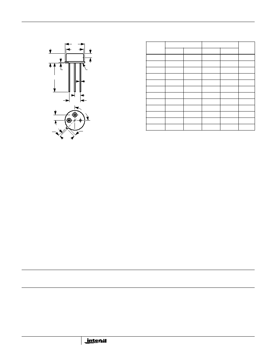
TO-205AF
3 LEAD JEDEC TO-205AF HERMETIC METAL CAN PACKAGE
L
A
Øb
ØD
1
ØD
h
1
2
3
e
e
1
SEATING
PLANE
90
o
e
2
j
k
P
45
o
SYMBOL
INCHES
MILLIMETERS
NOTES
MIN
MAX
MIN
MAX
A
0.160
0.180
4.07
4.57
-
Øb
0.016
0.021
0.41
0.53
2, 3
ØD
0.350
0.370
8.89
9.39
-
ØD
1
0.315
0.335
8.01
8.50
-
e
0.095
0.105
2.42
2.66
4
e
1
0.190
0.210
4.83
5.33
4
e
2
0.095
0.105
2.42
2.66
4
h
0.010
0.020
0.26
0.50
-
j
0.028
0.034
0.72
0.86
-
k
0.029
0.045
0.74
1.14
-
L
0.500
0.560
12.70
14.22
3
P
0.075
-
1.91
-
5
NOTES:
1. These dimensions are within allowable dimensions of Rev. E of
JEDEC TO-205AF outline dated 11-82.
2. Lead dimension (without solder).
3. Solder coating may vary along lead length, add typically 0.002
inches (0.05mm) for solder coating.
4. Position of lead to be measured 0.100 inches (2.54mm) from bottom
of seating plane.
5. This zone controlled for automatic handling. The variation in
actual diameter within this zone shall not exceed 0.010 inches
(0.254mm).
6. Lead no. 3 butt welded to stem base.
7. Controlling dimension: Inch.
8. Revision 3 dated 6-94.
JANSR2N7281