 | –≠–ª–µ–∫—Ç—Ä–æ–Ω–Ω—ã–π –∫–æ–º–ø–æ–Ω–µ–Ω—Ç: LM741N | –°–∫–∞—á–∞—Ç—å:  PDF PDF  ZIP ZIP |
1
CA741, CA741C, CA1458, CA1558,
LM741, LM741C, LM1458
0.9MHz Single and Dual, High Gain
Operational Amplifiers for Military,
Industrial and Commercial Applications
The CA1458, CA1558 (dual types); CA741C, CA741 (single
types); high-gain operational amplifiers for use in military,
industrial, and commercial applications.
These monolithic silicon integrated circuit devices provide
output short circuit protection and latch-free operation.
These types also feature wide common mode and
differential mode signal ranges and have low offset voltage
nulling capability when used with an appropriately valued
potentiometer. A 10k
potentiometer is used for offset
nulling types CA741C, CA741 (see Figure 1). Types
CA1458, CA1558 have no specific terminals for offset
nulling. Each type consists of a differential input amplifier
that effectively drives a gain and level shifting stage having
a complementary emitter follower output.
The manufacturing process make it possible to produce IC
operational amplifiers with low burst "popcorn'' noise
characteristics.
Technical Data on LM Branded types is identical to the
corresponding CA Branded types.
Features
∑ Input Bias Current . . . . . . . . . . . . . . . . . . . . 500nA (Max)
∑ Input Offset Current . . . . . . . . . . . . . . . . . . . 200nA (Max)
Applications
∑ Comparator
∑ Multivibrator
∑ DC Amplifier
∑ Summing Amplifier
∑ Integrator or Differentiator
∑ Narrow Band or Band Pass Filter
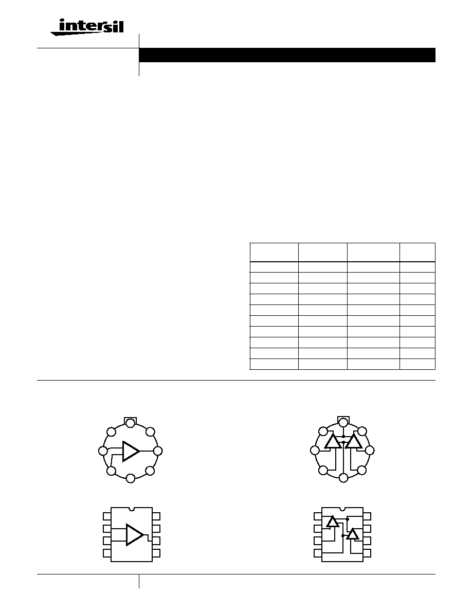
Pinouts
Ordering Information
PART
NUMBER
TEMP. RANGE
(
o
C)
PACKAGE
PKG. NO.
CA0741E
-55 to 125
8 Ld PDIP
E8.3
CA0741CE
0 to 70
8 Ld PDIP
E8.3
CA1458E
0 to 70
8 Ld PDIP
E8.3
CA1558E
-55 to 125
8 Ld PDIP
E8.3
CA0741T
-55 to 125
8 Pin Metal Can
T8.C
CA0741CT
0 to 70
8 Pin Metal Can
T8.C
CA1558T
-55 to 125
8 Pin Metal Can
T8.C
LM741N
-55 to 125
8 Ld PDIP
E8.3
LM741CN
0 to 70
8 Ld PDIP
E8.3
LM1458N
0 to 70
8 Ld PDIP
E8.3
CA741, CA741C (CAN)
TOP VIEW
CA1558 (METAL CAN)
TOP VIEW
CA741, CA741C, LM741, LM741C (PDIP)
TOP VIEW
CA1458, CA1558, LM1458 (PDIP)
TOP VIEW
NC
OUT
INV.
V-
OFFSET
NON-INV.
V+
OFFSET
2
4
6
1
3
7
5
8
-
+
NULL
INPUT
INPUT
NULL
V+
INV. INPUT
INV. INPUT
V-
OUTPUT
NON-INV.
OUTPUT
NON-INV.
2
4
6
1
3
7
5
8
-
(B)
(B)
INPUT (B)
INPUT (A)
(A)
(A)
A
B
+
-
+
OFFSET NULL
INV. INPUT
NON-INV. INPUT
V-
1
2
3
4
8
7
6
5
NC
V+
OUTPUT
OFFSET NULL
-
+
OUTPUT (A)
INV. INPUT (A)
NON-INV. INPUT (A)
V-
1
2
3
4
8
7
6
5
V+
OUTPUT (B)
INV. INPUT (B)
NON-INV. INPUT (B)
A
B
Data Sheet
September 1998
File Number
531.4
CAUTION: These devices are sensitive to electrostatic discharge; follow proper IC Handling Procedures.
1-888-INTERSIL or 321-724-7143
|
Copyright
©
Intersil Corporation 1999
2
Absolute Maximum Ratings
Thermal Information
Supply Voltage
CA741C, CA1458, LM741C, LM1458 (Note 1) . . . . . . . . . . . 36V
CA741, CA1558, LM741 (Note 1) . . . . . . . . . . . . . . . . . . . . . 44V
Differential Input Voltage . . . . . . . . . . . . . . . . . . . . . . . . . . . . . . 30V
Input Voltage . . . . . . . . . . . . . . . . . . . . . . . . . . . . . . . . . .
±
V
SUPPLY
Offset Terminal to V- Terminal Voltage (CA741C, CA741) . . . .
±
0.5V
Output Short Circuit Duration. . . . . . . . . . . . . . . . . . . . . . . Indefinite
Operating Conditions
Temperature Range
CA741, CA1558, LM741 . . . . . . . . . . . . . . . . . . . -55
o
C to 125
o
C
CA741C, CA1458, LM741C, LM1458 (Note 2) . . . . 0
o
C to 70
o
C
Thermal Resistance (Typical, Note 3)
JA
(
o
C/W)
JC
(
o
C/W)
PDIP Package . . . . . . . . . . . . . . . . . . .
130
N/A
Can Package . . . . . . . . . . . . . . . . . . . .
155
67
Maximum Junction Temperature (Can Package) . . . . . . . . . . 175
o
C
Maximum Junction Temperature (Plastic Package) . . . . . . . . 150
o
C
Maximum Storage Temperature Range . . . . . . . . . . -65
o
C to 150
o
C
Maximum Lead Temperature (Soldering 10s) . . . . . . . . . . . . 300
o
C
CAUTION: Stresses above those listed in "Absolute Maximum Ratings" may cause permanent damage to the device. This is a stress only rating and operation of the
device at these or any other conditions above those indicated in the operational sections of this specification is not implied.
NOTES:
1. Values apply for each section of the dual amplifiers.
2. All types in any package style can be operated over the temperature range of -55
o
C to 125
o
C, although the published limits for certain electrical
specification apply only over the temperature range of 0
o
C to 70
o
C.
3.
JA
is measured with the component mounted on an evaluation PC board in free air.
Electrical Specifications
Typical Values Intended Only for Design Guidance, V
SUPPLY
=
±
15V
PARAMETER
SYMBOL
TEST CONDITIONS
TYPICAL VALUE
(ALL TYPES)
UNITS
Input Capacitance
C
I
1.4
pF
Offset Voltage Adjustment Range
±
15
mV
Output Resistance
R
O
75
Output Short Circuit Current
25
mA
Transient Response
Unity Gain, V
I
= 20mV, R
L
= 2k
,
C
L
100pF
Rise Time
tr
0.3
µ
s
Overshoot
O.S.
5.0
%
Slew Rate (Closed Loop)
SR
R
L
2k
0.5
V/
µ
s
Gain Bandwidth Product
GBWP
R
L
= 12k
0.9
MHz
Electrical Specifications
For Equipment Design, V
SUPPLY
=
±
15V
PARAMETER
TEST
CONDITIONS
TEMP
(
o
C)
(NOTE 4)
CA741, CA1558, LM741
(NOTE 4)
CA741C, CA1458, LM741C,
LM1458
UNITS
MIN
TYP
MAX
MIN
TYP
MAX
Input Offset Voltage
R
S
10k
25
-
1
5
-
2
6
mV
Full
-
1
6
-
-
7.5
mV
Input Common Mode Voltage Range
25
-
-
-
±
12
±
13
-
V
Full
±
12
±
13
-
-
-
-
V
Common Mode Rejection Ratio
R
S
10k
25
-
-
-
70
90
-
dB
Full
70
90
-
-
-
-
dB
Power Supply Rejection Ratio
R
S
10k
25
-
-
-
-
30
150
µ
V/V
Full
-
30
150
-
-
-
µ
V/V
Input Resistance
25
0.3
2
-
0.3
2
-
M
CA741, CA741C, CA1458, CA1558, LM741, LM741C, LM1458
3
Input Bias Current
25
-
80
500
-
80
500
nA
Full
-
-
-
-
-
800
nA
-55
-
300
1500
-
-
-
nA
125
-
30
500
-
-
-
nA
Input Offset Current
25
-
20
200
-
20
200
nA
Full
-
-
-
-
-
300
nA
-55
-
85
500
-
-
-
nA
125
-
7
200
-
-
-
nA
Large Signal Voltage Gain
R
L
2k
, V
O
=
±
10V
25
50,000
200,000
-
20,000
200,000
-
V/V
Full
25,000
-
-
15,000
-
-
V/V
Output Voltage Swing
R
L
10k
25
-
-
-
±
12
±
14
-
V
Full
±
12
±
14
-
-
-
-
V
R
L
2k
25
-
-
-
±
10
±
13
-
V
Full
±
10
±
13
-
±
10
±
13
-
V
Supply Current
25
-
1.7
2.8
-
1.7
2.8
mA
-55
-
2
3.3
-
-
-
mA
125
-
1.5
2.5
-
-
-
mA
Device Power Dissipation
25
-
50
85
-
50
85
mW
-55
-
60
100
-
-
-
mW
125
-
45
75
-
-
-
mW
NOTE:
4. Values apply for each section of the dual amplifiers.
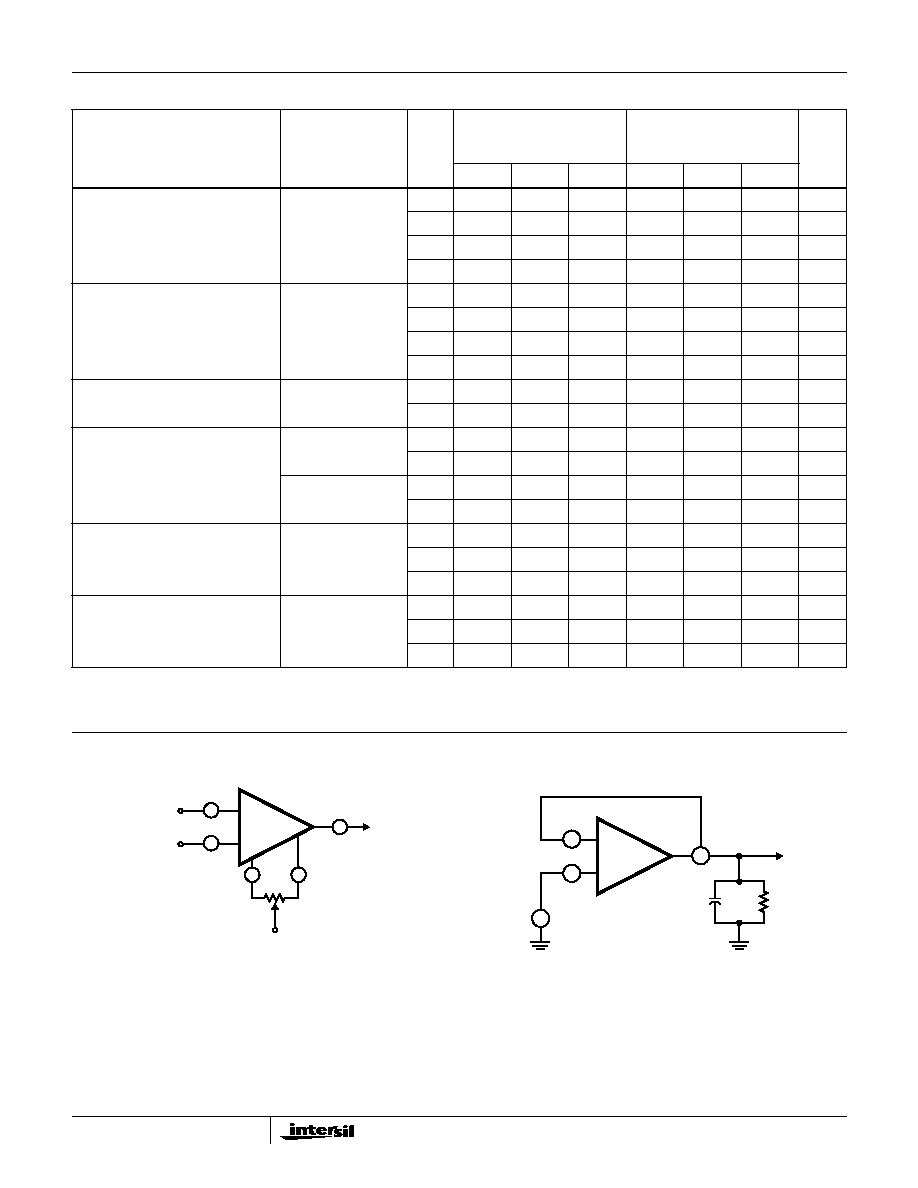
Test Circuits
FIGURE 1. OFFSET VOLTAGE NULL CIRCUIT FOR CA741C,
CA741, LM741C, AND LM741
FIGURE 2. TRANSIENT RESPONSE TEST CIRCUIT FOR ALL
TYPES
Electrical Specifications
For Equipment Design, V
SUPPLY
=
±
15V (Continued)
PARAMETER
TEST
CONDITIONS
TEMP
(
o
C)
(NOTE 4)
CA741, CA1558, LM741
(NOTE 4)
CA741C, CA1458, LM741C,
LM1458
UNITS
MIN
TYP
MAX
MIN
TYP
MAX
-
+
INVERTING
INPUT
NON-INVERTING
INPUT
OUTPUT
V-
OFFSET
NULL
10k
2
3
1
5
6
-
+
V
IN
C
L
R
L
V
OUT
CA741, CA741C, CA1458, CA1558, LM741, LM741C, LM1458
4
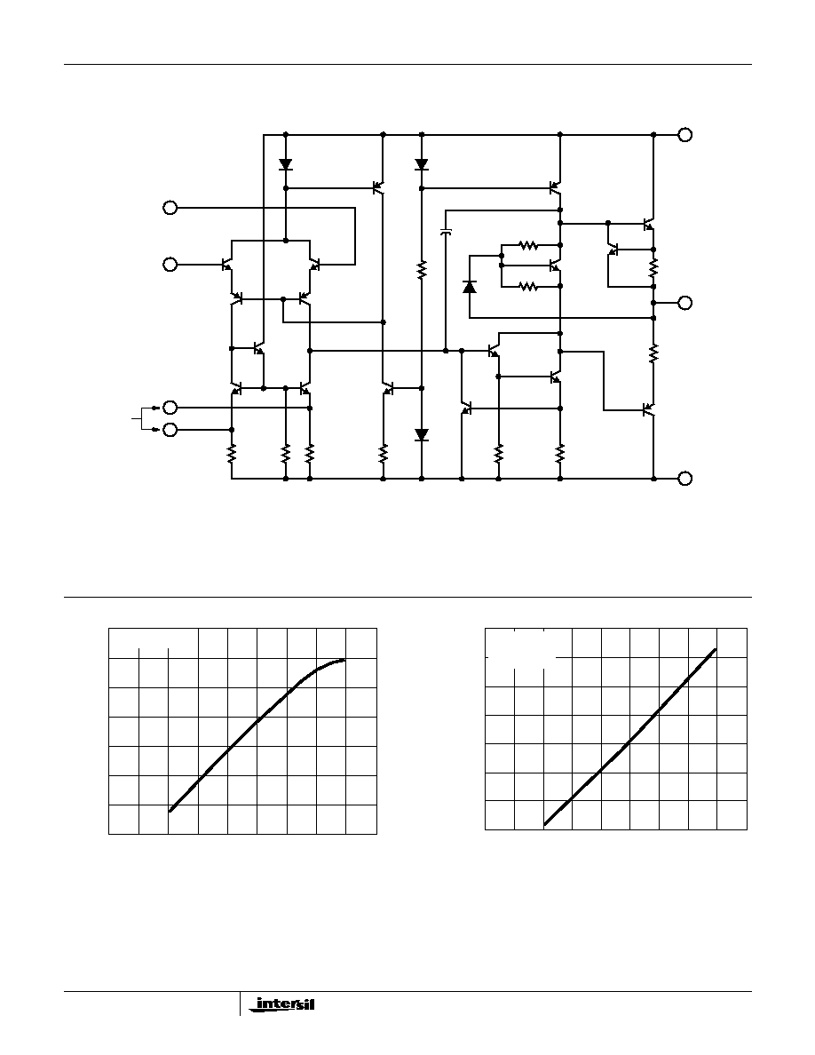
Schematic Diagram
(Notes 5, 6)
CA741C, CA741, LM741C, LM741 AND FOR EACH AMPLIFIER OF THE CA1458, CA1558, AND LM1458
Typical Performance Curves
FIGURE 3. COMMON MODE INPUT VOLTAGE RANGE vs SUPPLY
VOLTAGE FOR ALL TYPES
FIGURE 4. OUTPUT VOLTAGE vs SUPPLY VOLTAGE FOR ALL
TYPES
INVERTING
NON-INVERTING
INPUT
INPUT
OFFSET
NULL
*
R
1
1K
R
3
50K
R
2
1K
Q
6
Q
7
Q
8
Q
3
Q
1
Q
4
Q
2
R
4
3K
Q
9
R
5
39K
R
7
4.5K
R
8
7.5K
D
4
C
1
30pF
Q
11
Q
10
D
1
D
2
Q
5
D
3
Q
14
Q
15
Q
16
R
12
50K
R
11
80K
V+
OUTPUT
V-
Q
12
Q
13
R
9
25
R
10
50
Q
17
NOTES:
5. See Pinouts for Terminal Numbers of Respective Types.
6. All Resistance Values are in Ohms.
*
*
*
*
*
*
15
10
5
0
0
5
10
15
20
COMMON MODE INPUT RANGE (V)
DC SUPPLY (V+, V-)
T
A
= 25
o
C
OUTPUT SWING (V
P-P
)
40
35
30
25
20
15
10
5
0
0
5
10
15
20
DC SUPPLY (V+, V-)
T
A
= 25
o
C
R
L
2k
CA741, CA741C, CA1458, CA1558, LM741, LM741C, LM1458
5
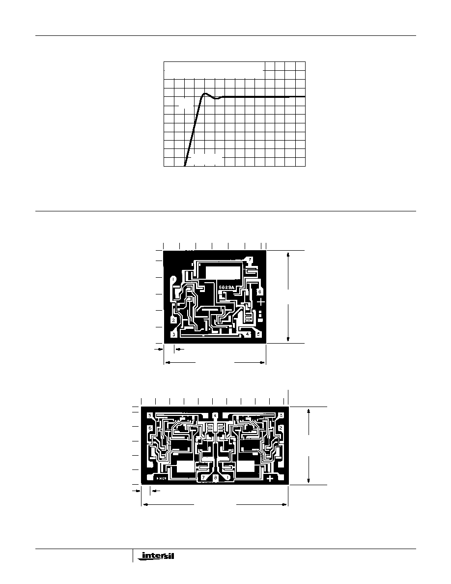
FIGURE 5. TRANSIENT RESPONSE FOR CA741C AND CA741
Metallization Mask Layout
CA741CH
CA1458H
NOTE: Dimensions in parentheses are in millimeters and are derived from the basic inch dimensions as indicated. Grid graduations are in mils (10
-
3
inch).
Typical Performance Curves
(Continued)
OUTPUT (mV)
30
25
20
15
20
5
0
-0.5
0
-0.5
1.0
1.5
2.0
2.5
3.0
TIME (
µ
s)
10%
RISE TIME
90%
DC SUPPLY VOLTS (V+ = 15, V- = -15)
T
A
= 25
o
C, C
L
= 100pF
0
10
20
30
40
50
60 64
54 - 62
(1.372 - 1.575)
61 - 69
(1.549 - 1.753)
4 - 10
(0.102 - 0.254)
57
50
40
30
20
10
0
55
50
40
30
20
10
0
60
0
10
20
30
40
50
70
80
100
104
90
101 - 109
(2.565 - 2.768)
4 - 10
(0.102 - 0.254)
52 - 60
(1.321 - 1.524)
CA741, CA741C, CA1458, CA1558, LM741, LM741C, LM1458

6
All Intersil semiconductor products are manufactured, assembled and tested under ISO9000 quality systems certification.
Intersil semiconductor products are sold by description only. Intersil Corporation reserves the right to make changes in circuit design and/or specifications at any time with-
out notice. Accordingly, the reader is cautioned to verify that data sheets are current before placing orders. Information furnished by Intersil is believed to be accurate and
reliable. However, no responsibility is assumed by Intersil or its subsidiaries for its use; nor for any infringements of patents or other rights of third parties which may result
from its use. No license is granted by implication or otherwise under any patent or patent rights of Intersil or its subsidiaries.
For information regarding Intersil Corporation and its products, see web site www.intersil.com
Sales Office Headquarters
NORTH AMERICA
Intersil Corporation
P. O. Box 883, Mail Stop 53-204
Melbourne, FL 32902
TEL: (321) 724-7000
FAX: (321) 724-7240
EUROPE
Intersil SA
Mercure Center
100, Rue de la Fusee
1130 Brussels, Belgium
TEL: (32) 2.724.2111
FAX: (32) 2.724.22.05
ASIA
Intersil (Taiwan) Ltd.
7F-6, No. 101 Fu Hsing North Road
Taipei, Taiwan
Republic of China
TEL: (886) 2 2716 9310
FAX: (886) 2 2715 3029
CA741, CA741C, CA1458, CA1558, LM741, LM741C, LM1458