1
Æ
TB423
CAUTION: These devices are sensitive to electrostatic discharge; follow proper IC Handling Procedures.
1-888-INTERSIL or 321-724-7143
|
Intersil (and design) is a registered trademark of Intersil Americas Inc.
Copyright © Intersil Americas Inc. 2004. All Rights Reserved. Elantec is a registered trademark of Elantec Semiconductor, Inc.
All other trademarks mentioned are the property of their respective owners.
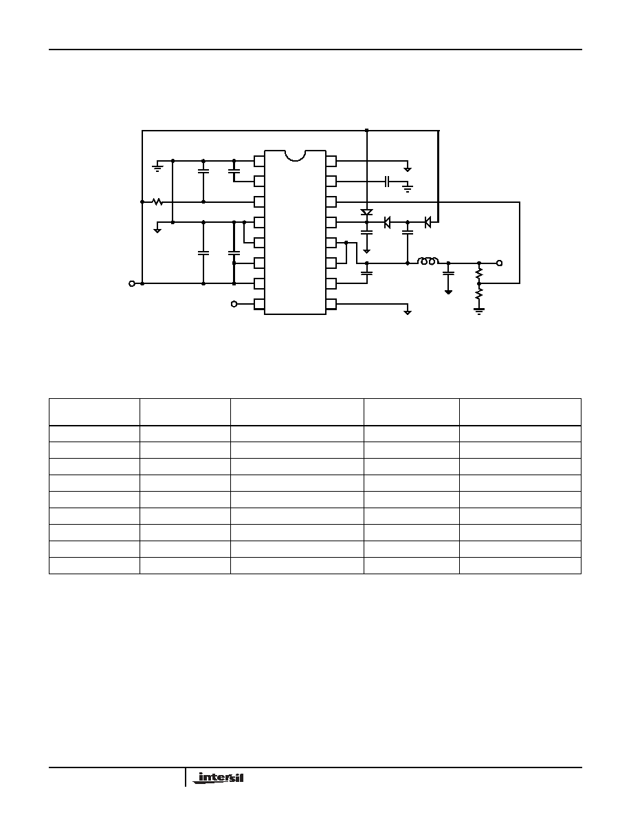
Using the EL7562 Demo Board
The EL7562 is a Buck (Step Down)
DC:DC controller with integrated
synchronous MOSFETs in a 16-pin
QSOP package. With very few external components, a 2A
step-down DC:DC converter can be very easily built,
resulting in saved board space (0.5in
2
), minimal design
effort, and improved design time.
There are 2 demo boards, one for nominal 5V input and
another for 3.3V input. This document outlines the design
consideration and lists the bill of materials and the layout.
Please also refer to the advanced data sheet of EL7562 for
detailed applications of the features.
EL7562 Demo Board Circuit Schematic for V
IN
= 5V Application
EL7562
1
2
3
4
16
15
14
13
5
6
7
12
11
10
8
9
SGND
COSC
VDD
PGND
PGND
VIN
VIN
EN
PGND
VREF
FB
VDRV
LX
LX
VHI
PGND
R
3
R
2
L
1
C
3
C
4
C
1
C
2
C
5
R
1
C
6
C
7
V
O
V
IN
V
O
0.985
1
R
2
R
1
-------
+
◊
=
EL7562 Demo Board Bill of Material
V
IN
= 5V, V
OUT
= 3.3V
REFERENCE
DESIGNATION
VALUE
MANUFACTURER
MANUFACTURER'S
PHONE NUMBER
PART NUMBER
C1
100µF
Sprague
207-324-4140
293D107X0010D2
C2, C3, C5, C6
0.1µF, 0603
Any
C4
270pF, 5%, 0603
Any
C7
100µF
Sprague
207-324-4140
293D107X0010D2
L1
4.7µH
Coilcraft
847-639-6400
D01813472HC
R1
1k
, 0603
Any
R2
2370
, 0603
Any
R3
39
, 0603
Any
Technical Brief
June 20, 2002
NOT
REC
OMM
END
ED F
OR N
EW
DES
IGNS
SEE
EL7
532

3
Design Considerations
Choosing the Component Values
The following requirements are specified for a DC:DC
converter:
∑ Input voltage range: V
IN
= 4.5V-5.5V
∑ Output voltage: V
O
= 3.3V
∑ Max output voltage ripple:
V
O
= 50mV
∑ Output max current: I
O
= 2A
The following steps briefly outline the steps to choose
components.
1. Choose the feedback resister divider.
The output voltage is decided by:
2. Choose the converter switching frequency F
S
.
F
S
, inductor L
1
, output capacitor C
7
, and EL7562's
switching loss are closely related. many iterations (or
thermal measurements) may be required before a final
value can be decided.
Please refer to the EL7562 data sheet for the F
S
vs
C
OSC
curve.
3. Inductor L
1
.
The EL7562 is internally ramp-compensated. For
optimal operation, the inductor current ripple should be
less than 0.6A.
If
I
L
= 0.5A, then:
where:
Choosing L
1
= 4.7µH yields
I
LMAX
= 0.56A. L
1
should
also be able to handle DC current of 2A and peak
current of 2.3A at temperature range.
4. Output capacitor C
7
.
V
O
and
I
L
normally decide C
7
value.
V
O
requires
ESR of C
7
be less than:
Double-check the RMS current requirement of the output
capacitor:
which is 0.16A. For a capacitor or combination of
capacitors with 89m
parallel ESR, it is more than
enough to handle this current.
5. Input capacitors C
1
and C
2
.
If all the AC current is handled by the input capacitors its
RMS current is calculated as:
This gives almost 0.99A when D = D
MAX
. Therefore a
cap with 0.99A current handling capability should be
chosen. However, in case some other capacitor is
sharing current with it, this current requirement can be
reduced.
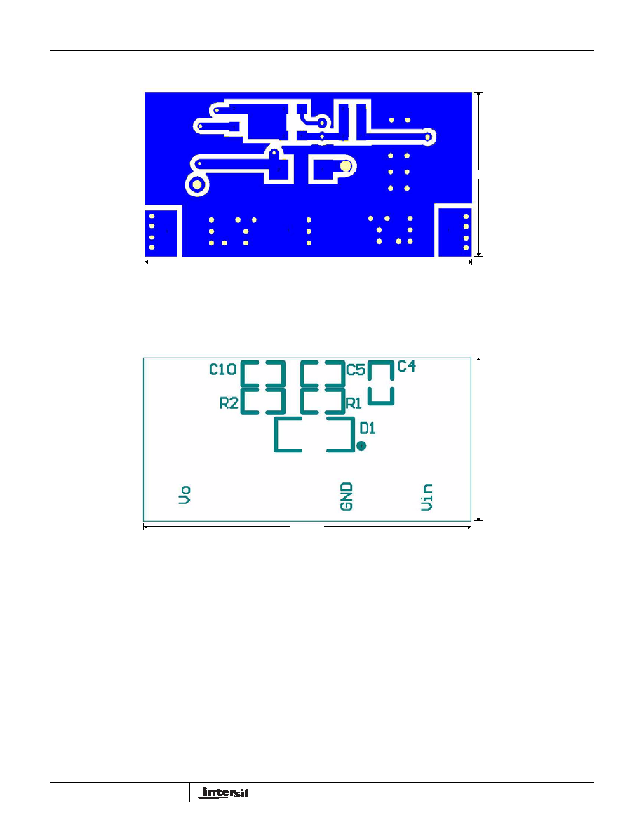
Layout Considerations
The layout is very important for the converter to function
properly. Power Ground ( ) and Signal Ground ( ) should
be separated to ensure that the high pulse current in the
Power Ground never interferes with the sensitive signals
connected to Signal Ground. They should only be connected
at one point (normally at the negative side of either the input
or output capacitor.)
The trace connected to pin 14 (FB) is the most sensitive
trace. It needs to be as short as possible and in a "quiet"
place, preferably between the PGND and SGND traces.
In addition, the bypass capacitor C
3
should be as close to
pins 1 and 3 as possible.
The heat of the chip is mainly dissipated through the PGND
pins. Maximizing the copper area around these pins is
preferable. In addition, a solid ground plane is always helpful
for the EMI performance.
V
OUT
0.985
1
R
2
R
1
-------
+
◊
=
For V
IN
= 5V
V
OUT
0.975
1
R
2
R
1
-------
+
◊
=
For V
IN
= 3.3V
L
1
(
D
)
V
O
◊
≠
I
L
F
S
◊
----------------------------------
=
D
V
O
V
IN
---------
=
ESR
V
O
I
LMAX
---------------------
89m
=
=
I
C7
I
LMAX
12
---------------------
=
I
IN,rms
D
[
1
(
D
) ]
≠
◊
I
O
◊
=
Technical Brief 423
7
Intersil Corporation reserves the right to make changes in circuit design, software and/or specifications at any time without notice. Accordingly, the reader is cautioned to
verify that the Application Note or Technical Brief is current before proceeding.
For information regarding Intersil Corporation and its products, see www.intersil.com
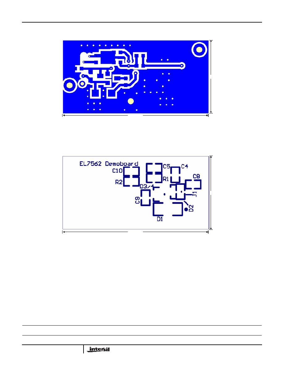
FIGURE 7. BOTTOM LAYER
FIGURE 8. BOTTOM SILKSCREEN
Demo Board Layout for V
IN
= 3.3V
(Continued)
1.2"
0.6"
1.2"
0.6"
Technical Brief 423