1
Æ
FN8106.1
CAUTION: These devices are sensitive to electrostatic discharge; follow proper IC Handling Procedures.
1-888-INTERSIL or 1-888-468-3774
|
Intersil (and design) is a registered trademark of Intersil Americas Inc.
Copyright Intersil Americas Inc. 2005. All Rights Reserved
All other trademarks mentioned are the property of their respective owners.
X28C512, X28C513
5V, Byte Alterable EEPROM
The X28C512, X28C513 are 64K x 8 EEPROM, fabricated
with Intersil's proprietary, high performance, floating gate
CMOS technology. Like all Intersil programmable nonvolatile
memories, the X28C512, X28C513 are 5V only devices. The
X28C512, X28C513 feature the JEDEC approved pin out for
byte wide memories, compatible with industry standard
EPROMS.
The X28C512, X28C513 support a 128-byte page write
operation, effectively providing a 39µs/byte write cycle and
enabling the entire memory to be written in less than 2.5
seconds. The X28C512, X28C513 also feature DATA Polling
and Toggle Bit Polling, system software support schemes
used to indicate the early completion of a write cycle. In
addition, the X28C512, X28C513 support the software data
protection option.
Features
∑ Access Time: 90ns
∑ Simple Byte and Page Write
- Single 5V supply
∑ No external high voltages or V
PP
control circuits
- Self-timed
∑ No erase before write
∑ No complex programming algorithms
∑ No overerase problem
∑ Low Power CMOS
- Active: 50mA
- Standby: 500µA
∑ Software Data Protection
- Protects data against system level inadvertent writes
∑ High Speed Page Write Capability
∑ Highly Reliable Direct Write
TM
Cell
- Endurance: 100,000 write cycles
- Data retention: 100 years
- Early end of write detection
- DATA polling
- Toggle bit polling
∑ Two PLCC and LCC Pinouts
- X28C512
∑ X28C010 EPROM pin compatible
- X28C513
∑ Compatible with lower density EEPROMs
∑ Pb-Free Plus Anneal Available (RoHS Compliant)
Data Sheet
September 29, 2005
5
FN8106.1
September 29, 2005
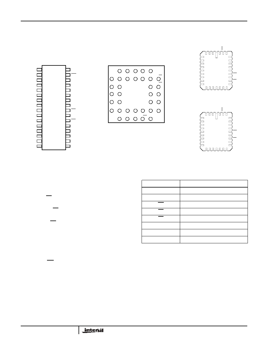
Pinouts
Pin Descriptions
Addresses (A
0
-A
15
)
The Address inputs select an 8-bit memory location during a
read or write operation.
Chip Enable (CE)
The Chip Enable input must be LOW to enable all read/write
operations. When CE is HIGH, power consumption is
reduced.
Output Enable (OE)
The Output Enable input controls the data output buffers and
is used to initiate read operations.
Data In/Data Out (I/O
0
-I/O
7
)
Data is written to or read from the X28C512, X28C513
through the I/O pins.
Write Enable (WE)
The Write Enable input controls the writing of data to the
X28C512, X28C513.
NC
NC
A
15
A
12
A
7
A
6
A
5
A
4
A
3
A
2
A
1
A
0
I/O
0
I/O
1
I/O
2
V
SS
1
2
3
4
5
6
7
8
9
10
11
12
13
14
15
16
32
31
30
29
28
27
26
25
24
23
22
21
20
19
18
17
V
CC
WE
NC
A
14
A
13
A
8
A
9
A
11
OE
A
10
CE
I/O
5
I/O
4
I/O
3
I/O
2
I/O
1
X28C512
Plastic DIP
CERDIP
FLAT Pack
SOIC (R)
Bottom
14
A
0
16
I/O
1
18
V
SS
11
A
3
9
A
5
7
A
7
15
I/O
0
17
I/O
2
19
I/O
3
5
A
15
2
NC
36
V
CC
20
I/O
4
21
I/O
5
34
NC
23
I/O
7
25
A
10
27
A
11
29
A
8
22
I/O
6
32
NC
24
CE
26
OE
28
A
9
30
A
13
13
A
1
12
A
2
10
A
4
8
A
6
4
NC
3
NC
1
NC
35
WE
33
NC
31
A
14
6
A
12
PGA
X28C512
A
7
A
6
A
5
A
4
A
3
A
2
A
1
A
0
I/O
0
A
13
A
8
A
9
A
11
OE
A
10
CE
I/O
7
A
14
I/O
1
A
12
A
15
NC
NC
V
CC
WE
NC
2 32
6
1
5 4 3
8
7
9
10
11
12
13 15 17
16 18
19
20
22
23
24
25
26
27
28
29
31
14
21
30
PLCC/LCC
I/O
2
V
SS
I/O
3
I/O
4
I/O
5
I/O
6
X28C513
A
6
A
5
A
4
A
3
A
2
A
1
A
0
NC
I/O
0
A
9
A
11
NC
OE
A
10
CE
I/O
6
A
8
I/O
1
A
7
A
12
V
CC
WE
2 32
6
1
5 4 3
8
7
9
10
11
12
13 15 17
16 18
19
20
22
23
24
25
26
27
28
29
31
14
21
30
I/O
2
V
SS
NC
I/O
3
I/O
4
I/O
5
A
14
A
15
A
13
I/O
7
View
(Top View)
(Top View)
Pin Names
SYMBOL
DESCRIPTION
A
0
-A
15
Address Inputs
I/O
0
-I/O
7
Data Input/Output
WE
Write Enable
CE
Chip Enable
OE
Output Enable
V
CC
+5V
V
SS
Ground
NC
No Connect
X28C512, X28C513