
1
Æ
FN8109.0
CAUTION: These devices are sensitive to electrostatic discharge; follow proper IC Handling Procedures.
1-888-INTERSIL or 1-888-468-3774
|
Intersil (and design) is a registered trademark of Intersil Americas Inc.
Copyright Intersil Americas Inc. 2005. All Rights Reserved
All other trademarks mentioned are the property of their respective owners.
X28HC64
64K, 8K x 8 Bit
5 Volt, Byte Alterable EEPROM
FEATURES
∑ 70ns access time
∑ Simple byte and page write
--Single 5V supply
--No external high voltages or V
PP
control circuits
--Self-timed
--No erase before write
--No complex programming algorithms
--No overerase problem
∑ Low power CMOS
--40mA active current max.
--200µA standby current max.
∑ Fast write cycle times
--64-byte page write operation
--Byte or page write cycle: 2ms typical
--Complete memory rewrite: 0.25 sec. typical
--Effective byte write cycle time: 32µs typical
∑ Software data protection
∑ End of write detection
--DATA polling
--Toggle bit
∑ High reliability
--Endurance: 1 million cycles
--Data retention: 100 years
∑ JEDEC approved byte-wide pin out
DESCRIPTION
The X28HC64 is an 8K x 8 EEPROM, fabricated with
Intersil's proprietary, high performance, floating gate
CMOS technology. Like all Intersil programmable non-
volatile memories, the X28HC64 is a 5V only device. It
features the JEDEC approved pinto for byte-wide mem-
ories, compatible with industry standard RAMs.
The X28HC64 supports a 64-byte page write operation,
effectively providing a 32µs/byte write cycle, and
enabling the entire memory to be typically written in 0.25
seconds. The X28HC64 also features DATA Polling and
Toggle Bit Polling, two methods providing early end of
write detection. In addition, the X28HC64 includes a
user-optional software data protection mode that further
enhances Intersil's hardware write protect capability.
Intersil EEPROMs are designed and tested for appli-
cations requiring extended endurance. Inherent data
retention is greater than 100 years.
PIN CONFIGURATIONS
NC
A
12
A
7
A
6
A
5
A
4
A
3
A
2
A
1
A
0
I/O
0
I/O
1
I/O
2
V
SS
1
2
3
4
5
6
7
8
9
10
11
12
13
14
28
27
26
25
24
23
22
21
20
19
18
17
16
15
V
CC
WE
NC
A
8
A
9
A
11
OE
A
10
CE
I/O
7
I/O
6
I/O
5
I/O
4
I/O
3
X28HC64
Plastic DIP
Flat Pack
CERDIP
SOIC
A
6
A
5
A
4
A
3
A
2
A
1
A
0
NC
I/O
0
A
8
A
9
A
11
NC
OE
A
10
CE
I/O
7
I/O
6
4 3 2 1 32 31 30
14 15 16 17 18 19 20
5
6
7
8
9
10
11
12
13
29
28
27
26
25
24
23
22
21
LCC
PLCC
A
7
I/O
1
I/O
2
V
SS
I/O
3
I/O
4
I/O
5
(Top View)
1
2
3
4
5
6
7
8
9
10
11
12
13
14
15
16
A 3
A 4
A 5
A 6
A 7
A 12
NC
VCC
NC
WE
A 8
A 9
A11
OE
32
31
30
29
28
27
26
25
24
23
22
21
20
19
18
17
A 2
A 1
A 0
I/O 0
I/O 1
I/O 2
NC
VSS
NC
I/O 3
I/O 4
I/O 5
I/O 6
I/O 7
CE
A10
A
12
NC
V
CC
WE
NC
X28HC64
X28HC64
11
I/O
0
10
A
0
14
V
SS
9
A
1
8
A
2
7
A
3
6
A
4
5
A
5
2
A
12
28
V
CC
12
I/O
1
13
I/O
2
15
I/O
3
4
A
6
3
A
7
1
16
I/O
4
20
CE
22
OE
24
A
9
17
I/O
5
27
WE
19
I/O
7
21
A
10
23
A
11
25
A
8
18
I/O
6
26
NC
(BOTTOM
VIEW)
PGA
NC
X28HC64
TSOP
NC
NC
NC
NC
Bottom View
Data Sheet
June 1, 2005
2
FN8109.0
June 1, 2005
PIN DESCRIPTIONS
Addresses (A
0
-A
12
)
The Address inputs select an 8-bit memory location
during a read or write operation.
Chip Enable (CE)
The Chip Enable input must be LOW to enable all
read/write operations. When CE is HIGH, power con-
sumption is reduced.
Output Enable (OE)
The Output Enable input controls the data output buff-
ers and is used to initiate read operations.
Data In/Data Out (I/O
0
-I/O
7
)
Data is written to or read from the X28HC64 through
the I/O pins.
Write Enable (WE)
The Write Enable input controls the writing of data to
the X28HC64.
PIN NAMES
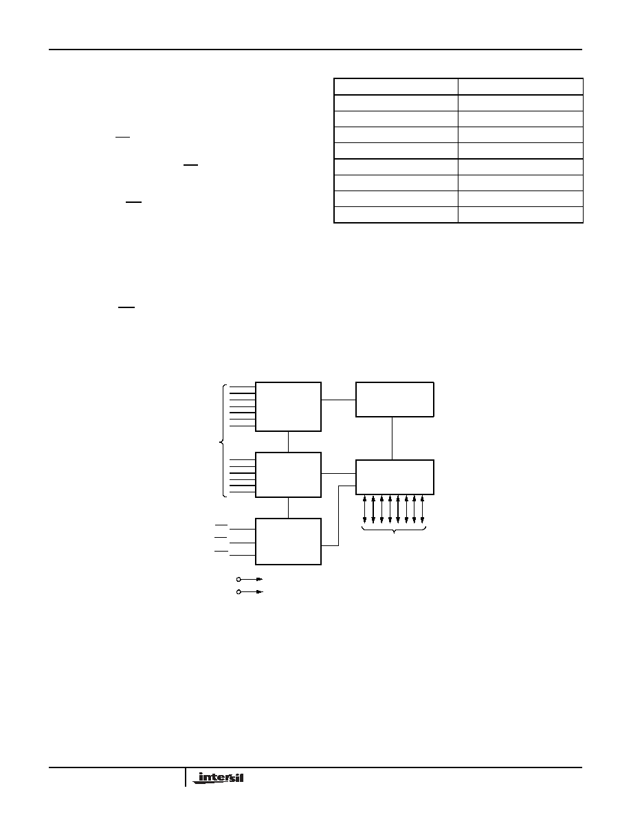
BLOCK DIAGRAM
Symbol
Description
A
0
-A
12
Address Inputs
I/O
0
-I/O
7
Data Input/Output
WE
Write Enable
CE
Chip Enable
OE
Output Enable
V
CC
+5V
V
SS
Ground
NC
No Connect
X Buffers
Latches and
Decoder
I/O Buffers
and Latches
Y Buffers
Latches
Decoder
Control
Logic and
Timing
65,536-Bit
EEPROM
Array
I/O
0
≠I/O
7
Data Inputs/Outputs
CE
OE
V
CC
V
SS
A
0
≠A
12
WE
Address
Inputs
and
X28HC64
3
FN8109.0
June 1, 2005
DEVICE OPERATION
Read
Read operations are initiated by both OE and CE
LOW. The read operation is terminated by either CE or
OE returning HIGH. This two line control architecture
eliminates bus contention in a system environment.
The data bus will be in a high impedance state when
either OE or CE is HIGH.
Write
Write operations are initiated when both CE and WE
are LOW and OE is HIGH. The X28HC64 supports
both a CE and WE controlled write cycle. That is, the
address is latched by the falling edge of either CE or
WE, whichever occurs last. Similarly, the data is
latched internally by the rising edge of either CE or
WE, whichever occurs first. A byte write operation,
once initiated, will automatically continue to comple-
tion, typically within 2ms.
Page Write Operation
The page write feature of the X28HC64 allows the
entire memory to be written in 0.25 seconds. Page write
allows two to sixty-four bytes of data to be consecu-
tively written to the X28HC64 prior to the commence-
ment of the internal programming cycle. The host can
fetch data from another device within the system during
a page write operation (change the source address),
but the page address (A
6
through A
12
) for each subse-
quent valid write cycle to the part during this operation
must be the same as the initial page address.
The page write mode can be initiated during any write
operation. Following the initial byte write cycle, the
host can write an additional one to sixty-three bytes in
the same manner. Each successive byte load cycle,
started by the WE HIGH to LOW transition, must begin
within 100µs of the falling edge of the preceding WE. If
a subsequent WE HIGH to LOW transition is not
detected within 100µs, the internal automatic program-
ming cycle will commence. There is no page write win-
dow limitation. Effectively the page write window is
infinitely wide, so long as the host continues to access
the device within the byte load cycle time of 100µs.
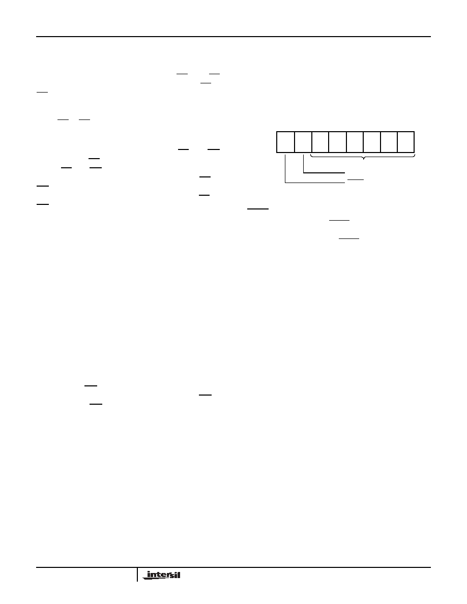
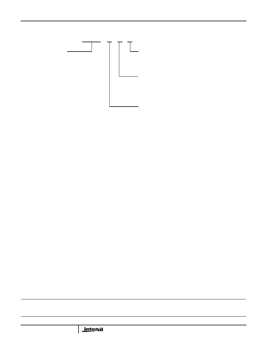
Write Operation Status Bits
The X28HC64 provides the user two write operation
status bits. These can be used to optimize a system
write cycle time. The status bits are mapped onto the
I/O bus as shown in Figure 1.
Figure 1. Status Bit Assignment
DATA Polling (I/O
7
)
The X28HC64 features DATA Polling as a method to
indicate to the host system that the byte write or page
write cycle has completed. DATA Polling allows a sim-
ple bit test operation to determine the status of the
X28HC64, eliminating additional interrupt inputs or
external hardware. During the internal programming
cycle, any attempt to read the last byte written will pro-
duce the complement of that data on I/O
7
(i.e. write
data = 0xxx xxxx, read data = 1xxx xxxx). Once the
programming cycle is complete, I/O
7
will reflect true data.
Toggle Bit (I/O
6
)
The X28HC64 also provides another method for deter-
mining when the internal write cycle is complete. Dur-
ing the internal programming cycle I/O
6
will toggle
from HIGH to LOW and LOW to HIGH on subsequent
attempts to read the device. When the internal cycle is
complete the toggling will cease and the device will be
accessible for additional read or write operations.
5
TB
DP
4
3
2
1
0
I/O
Reserved
Toggle Bit
DATA Polling
X28HC64
4
FN8109.0
June 1, 2005
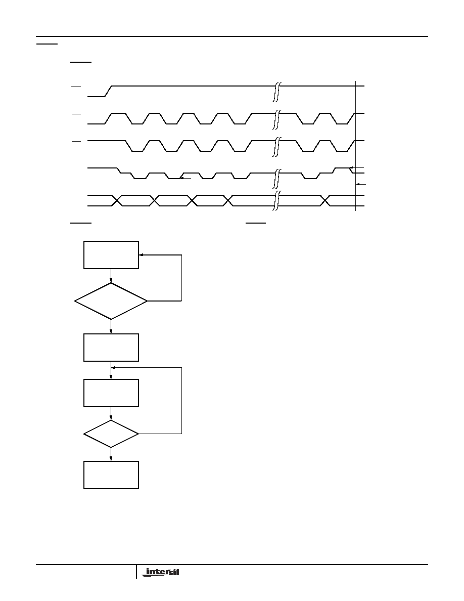
DATA POLLING I/O
7
Figure 2. DATA Polling Bus Sequence
Figure 3. DATA Polling Software Flow
DATA Polling can effectively reduce the time for writ-
ing to the X28HC64. The timing diagram in Figure 2
illustrates the sequence of events on the bus. The
software flow diagram in Figure 3 illustrates one
method of implementing the routine.
CE
OE
WE
I/O
7
X28HC64
Ready
Last
Write
HIGH Z
V
OL
V
IH
A
0
≠A
12
An
An
An
An
An
An
V
OH
An
Write Data
Save Last Data
and Address
Read Last
Address
IO
7
Compare?
No
Yes
Writes
Complete?
No
Yes
Ready
X28HC64

5
FN8109.0
June 1, 2005
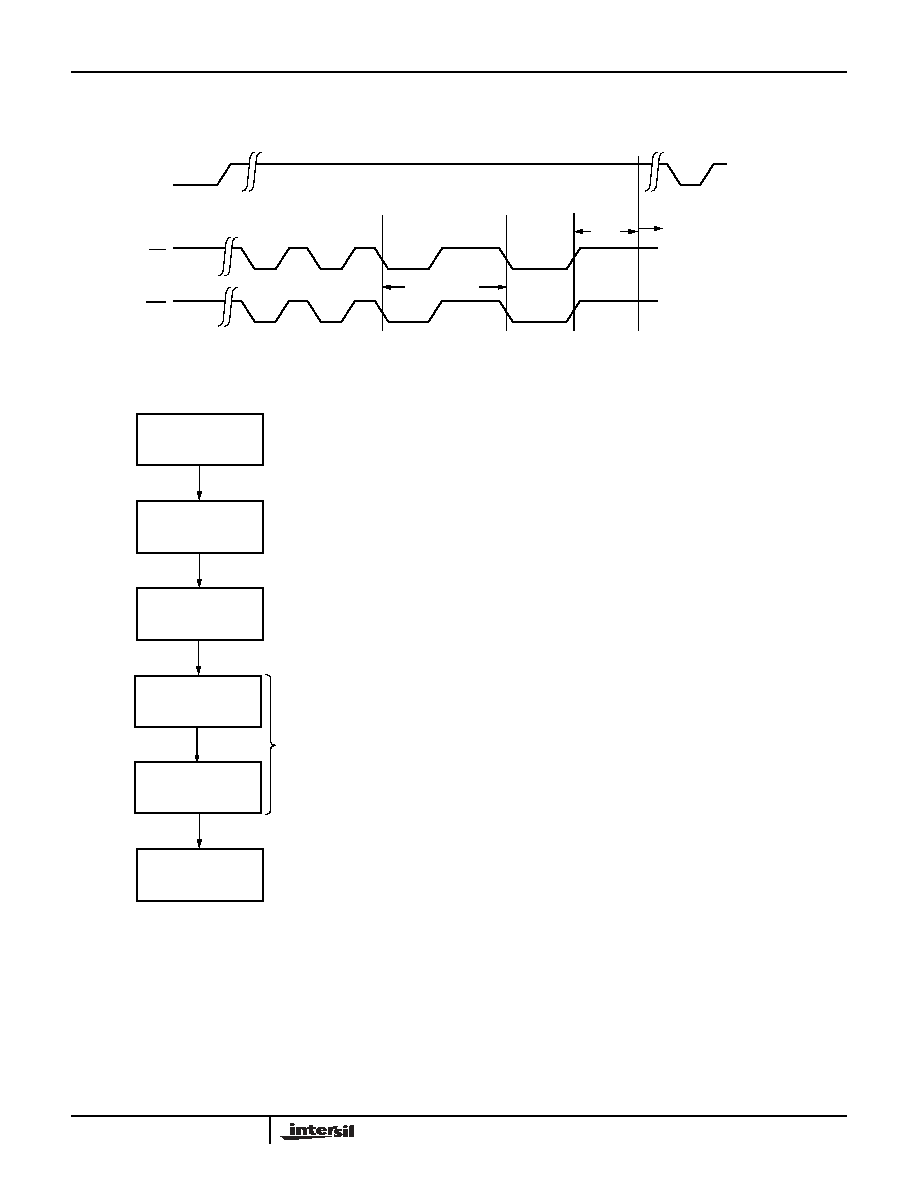
THE TOGGLE BIT I/O
6
Figure 4. Toggle Bit Bus Sequence
Figure 5. Toggle Bit Software Flow
The Toggle Bit can eliminate the chore of saving and
fetching the last address and data in order to implement
DATA Polling. This can be especially helpful in an array
comprised of multiple X28HC64 memories that is fre-
quently updated. Toggle Bit Polling can also provide a
method for status checking in multiprocessor applica-
tions. The timing diagram in Figure 4 illustrates the
sequence of events on the bus. The software flow dia-
gram in Figure 5 illustrates a method for polling the
Toggle Bit.
CE
OE
WE
X28HC64
Last
Write
I/O
6
HIGH Z
*
*
V
OH
V
OL
Ready
* Beginning and ending state of I/O
6
will vary.
Compare
No
Yes
Ok?
Compare
Accum with
Addr N
Load Accum
From Addr N
Last Write
Ready
Yes
X28HC64

6
FN8109.0
June 1, 2005
HARDWARE DATA PROTECTION
The X28HC64 provides two hardware features that
protect nonvolatile data from inadvertent writes.
≠ Default V
CC
Sense--All write functions are inhibited
when V
CC
is 3V typically.
≠ Write Inhibit--Holding either OE LOW, WE HIGH, or
CE HIGH will prevent an inadvertent write cycle dur-
ing power-up and power-down, maintaining data
integrity.
SOFTWARE DATA PROTECTION
The X28HC64 offers a software controlled data pro-
tection feature. The X28HC64 is shipped from Intersil
with the software data protection NOT ENABLED; that
is, the device will be in the standard operating mode.
In this mode data should be protected during power-
up/-down operations through the use of external cir-
cuits. The host would then have open read and write
access of the device once V
CC
was stable.
The X28HC64 can be automatically protected during
power-up and power-down without the need for exter-
nal circuits by employing the software data protection
feature. The internal software data protection circuit is
enabled after the first write operation utilizing the soft-
ware algorithm. This circuit is nonvolatile and will
remain set for the life of the device, unless the reset
command is issued.
Once the software protection is enabled, the X28HC64
is also protected from inadvertent and accidental
writes in the powered-up state. That is, the software
algorithm must be issued prior to writing additional
data to the device.
SOFTWARE ALGORITHM
Selecting the software data protection mode requires
the host system to precede data write operations by a
series of three write operations to three specific
addresses. Refer to Figure 6 and 7 for the sequence.
The three-byte sequence opens the page write window,
enabling the host to write from one to sixty-four bytes
of data. Once the page load cycle has been com-
pleted, the device will automatically be returned to the
data protected state.
X28HC64
7
FN8109.0
June 1, 2005
SOFTWARE DATA PROTECTION
Figure 6. Timing Sequence--Byte or Page Write
Figure 7. Write Sequence for Software
Data Protection
Regardless of whether the device has previously been
protected or not, once the software data protection
algorithm is used, the X28HC64 will automatically dis-
able further writes unless another command is issued
to deactivate it. If no further commands are issued the
X28HC64 will be write protected during power-down
and after any subsequent power-up.
Note: Once initiated, the sequence of write operations
should not be interrupted.
CE
WE
(V
CC
)
Write
Protected
V
CC
0V
Data
ADDR
AAA
1555
55
0AAA
A0
1555
t
BLC MAX
Writes
OK
Byte
or
Page
t
WC
Write Last
Write Data XX
to Any
Write Data A0
to Address
1555
Write Data 55
to Address
0AAA
Write Data AA
to Address
1555
After t
WC
Re-Enters Data
Protected State
Byte to
Last Address
Address
Optional
Byte/Page
Load Operation
Byte/Page
Load Enabled
X28HC64
8
FN8109.0
June 1, 2005
RESETTING SOFTWARE DATA PROTECTION
Figure 8. Reset Software Data Protection Timing Sequence
Figure 9. Software Sequence to Deactivate Software
Data Protection
In the event the user wants to deactivate the software
data protection feature for testing or reprogramming in
an EEPROM programmer, the following six step algo-
rithm will reset the internal protection circuit. After t
WC
,
the X28HC64 will be in standard operating mode.
Note: Once initiated, the sequence of write operations
should not be interrupted.
CE
WE
Standard
Operating
Mode
V
CC
Data
ADDR
AAA
1555
55
0AAA
80
1555
t
WC
AA
1555
55
0AAA
20
1555
Write Data 55
to Address
0AAA
Write Data 55
to Address
0AAA
Write Data 80
to Address
1555
Write Data AA
Address
1555
Write Data 20
to Address
1555
Write Data AA
to Address
1555
X28HC64

9
FN8109.0
June 1, 2005
SYSTEM CONSIDERATIONS
Because the X28HC64 is frequently used in large
memory arrays, it is provided with a two-line control
architecture for both read and write operations. Proper
usage can provide the lowest possible power dissipa-
tion, and eliminate the possibility of contention where
multiple I/O pins share the same bus.
To gain the most benefit, it is recommended that CE
be decoded from the address bus, and be used as the
primary device selection input. Both OE and WE would
then be common among all devices in the array. For a
read operation, this assures that all deselected
devices are in their standby mode, and that only the
selected device(s) is/are outputting data on the bus.
Because the X28HC64 has two power modes,
standby and active, proper decoupling of the memory
array is of prime concern. Enabling CE will cause tran-
sient current spikes. The magnitude of these spikes is
dependent on the output capacitive loading of the
I/Os. Therefore, the larger the array sharing a common
bus, the larger the transient spikes. The voltage peaks
associated with the current transients can be sup-
pressed by the proper selection and placement of
decoupling capacitors. As a minimum, it is recom-
mended that a 0.1µF high frequency ceramic capacitor
be used between V
CC
and V
SS
at each device.
Depending on the size of the array, the value of the
capacitor may have to be larger.
In addition, it is recommended that a 4.7µF electrolytic
bulk capacitor be placed between V
CC
and V
SS
for
each eight devices employed in the array. This bulk
capacitor is employed to overcome the voltage droop
caused by the inductive effects of the PC board traces.
Normalized I
CC
(RD) by Temperature
Over Frequency
Normalized I
CC
(RD) @ 25% Over
the V
CC
Range and Frequency
1.4
1.2
0.8
0.4
0.6
0.2
1.0
0
10
20
- 55∞C
+ 25∞C
Frequency (MHz)
+ 125∞C
5.5 V
CC
I
CC
RD
Norm
alize
d
(m
A)
1.4
1.2
0.8
0.4
0.6
0.2
1.0
0
10
20
Frequency (MHz)
4.5 V
CC
5.0 V
CC
5.5 V
CC
I
CC
RD
Nor
m
alized
(mA)
X28HC64
10
FN8109.0
June 1, 2005
ABSOLUTE MAXIMUM RATINGS
Temperature under bias
X28HC64 ......................................... -10∞C to +85∞C
X28HC64I, X28HC64M .................. -65∞C to +135∞C
Storage temperature ......................... -65∞C to +150∞C
Voltage on any pin with
respect to V
SS
......................................... -1V to +7V
D.C. output current ............................................... 5mA
Lead temperature
(soldering, 10 seconds).................................. 300∞C
COMMENT
Stresses above those listed under "Absolute Maximum
Ratings" may cause permanent damage to the device.
This is a stress rating only; functional operation of the
device (at these or any other conditions above those indi-
cated in the operational sections of this specification) is
not implied. Exposure to absolute maximum rating condi-
tions for extended periods may affect device reliability.
RECOMMENDED OPERATING CONDITIONS
D.C. OPERATING CHARACTERISTICS (Over recommended operating conditions unless otherwise specified.)
Notes: (1) Typical values are for T
A
= 25∞C and nominal supply voltage
(2) V
IL
min. and V
IH
max. are for reference only and are not tested.
Temperature
Min.
Max.
Commercial
0∞C
+70∞C
Industrial
-40∞C
+85∞C
Military
-55∞C
+125∞C
Supply Voltage
Limits
X28HC64
5V ±10%
Symbol
Parameter
Limits
Unit
Test Conditions
Min.
Typ.
(1)
Max.
I
CC
V
CC
current (active)
(TTL inputs)
15
40
mA
CE = OE = V
IL
, WE = V
IH
, All I/O's = open,
address inputs = TTL levels @ f = 10 MHz
I
SB1
V
CC
current (standby)
(TTL inputs)
1
2
mA
CE = V
IH
, OE = V
IL
All I/O's = open,
other inputs = V
IH
I
SB2
V
CC
current (standby)
(CMOS inputs)
100
200
µA
CE = V
CC
- 0.3V, OE = GND, All I/O's = open,
other inputs = V
CC
- 0.3V
I
LI
Input leakage current
±10
µA
V
IN
= V
SS
to V
CC
I
LO
Output leakage current
±10
µA
V
OUT
= V
SS
to V
CC
, CE = V
IH
V
lL
(2)
Input LOW voltage
-1
0.8
V
V
IH
(2)
Input HIGH voltage
2
V
CC
+ 1
V
V
OL
Output LOW voltage
0.4
V
I
OL
= 5mA
V
OH
Output HIGH voltage
2.4
V
I
OH
= -5mA
X28HC64

11
FN8109.0
June 1, 2005
ENDURANCE AND DATA RETENTION
POWER-UP TIMING
CAPACITANCE T
A
= +25∞C, f = 1MHz, V
CC
= 5V
A.C. CONDITIONS OF TEST
MODE SELECTION
Note:
(3) This parameter is periodically sampled and not 100% tested.
EQUIVALENT A.C. LOAD CIRCUITS
SYMBOL TABLE
Parameter
Min.
Max.
Unit
Minimum endurance
100,000
Cycles
Data retention
100
Years
Symbol
Parameter
Typ.
(1)
Unit
t
PUR
(3)
Power-up to read operation
100
µs
t
PUW
(3)
Power-up to write operation
5
ms
Symbol
Parameter
Max.
Unit
Test Conditions
C
I/O
(3)
Input/output capacitance
10
pF
V
I/O
= 0V
C
IN
(3)
Input capacitance
6
pF
V
IN
= 0V
Input pulse levels
0V to 3V
Input rise and fall times
5ns
Input and output timing levels
1.5V
CE OE WE
Mode
I/O
Power
L
L
H
Read
D
OUT
Active
L
H
L
Write
D
IN
Active
H
X
X
Standby and
write inhibit
High Z
Standby
X
L
X
Write inhibit
--
--
X
X
H
Write inhibit
--
--
5V
1.92k
30pF
Output
1.37k
WAVEFORM
INPUTS
OUTPUTS
Must be
steady
Will be
steady
May change
from LOW
to HIGH
Will change
from LOW
to HIGH
May change
from HIGH
to LOW
Will change
from HIGH
to LOW
Don't Care:
Changes
Allowed
Changing:
State Not
Known
N/A
Center Line
is High
Impedance
X28HC64
12
FN8109.0
June 1, 2005
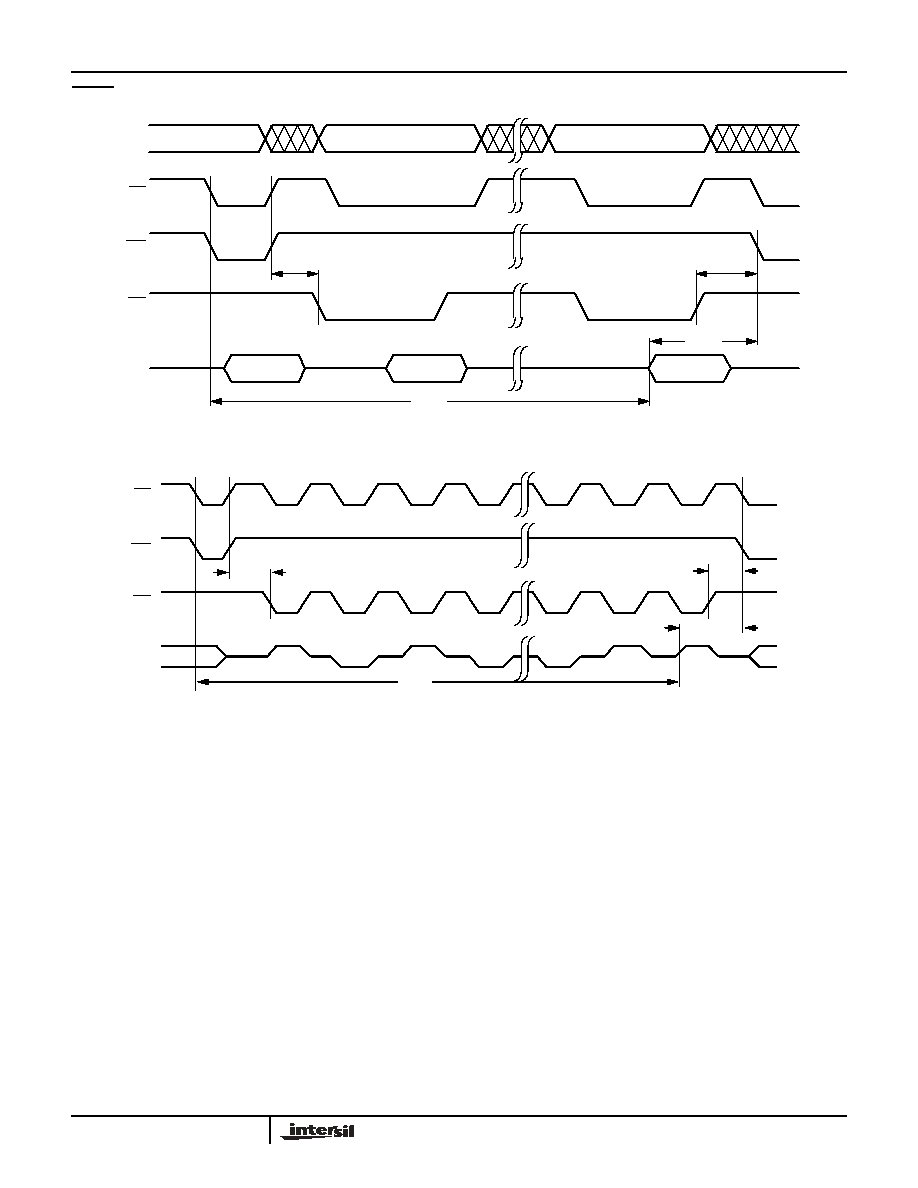
A.C. CHARACTERISTICS (Over the recommended operating conditions unless otherwise specified.)
Read Cycle Limits
Read Cycle
Note:
(4) t
LZ
min., t
HZ
, t
OLZ
min., and t
OHZ
are periodically sampled and not 100% tested. t
HZ
max. and t
OHZ
max. are measured from the point
when CE or OE return HIGH (whichever occurs first) to the time when the outputs are no longer driven.
Symbol
Parameter
X28HC64-70
X28HC64-90
X28HC64-12
Unit
-55∞C to +125∞C
-55∞C to +125∞C
-55∞C to +125∞C
Min.
Max.
Min.
Max.
Min.
Max.
t
RC
Read cycle time
70
90
120
ns
t
CE
Chip enable access time
70
90
120
ns
t
AA
Address access time
70
90
120
ns
t
OE
Output enable access time
35
40
50
ns
t
LZ
(4)
CE LOW to active output
0
0
0
ns
t
OLZ
(4)
OE LOW to active output
0
0
0
ns
t
HZ
(4)
CE HIGH to high Z output
30
30
30
ns
t
OHZ
(4)
OE HIGH to high Z output
30
30
30
ns
t
OH
Output hold from address change
0
0
0
ns
t
CE
t
RC
Address
CE
OE
WE
Data Valid
t
OE
t
LZ
t
OLZ
t
OH
t
AA
t
HZ
t
OHZ
Data I/O
V
IH
HIGH Z
Data Valid
X28HC64
13
FN8109.0
June 1, 2005
WRITE CYCLE LIMITS
WE Controlled Write Cycle
Notes: (5) t
WC
is the minimum cycle time to be allowed from the system perspective unless polling techniques are used. It is the maximum time
the device requires to automatically complete the internal write operation.
(6) t
WPH
and t
DW
are periodically sampled and not 100% tested.
Symbol
Parameter
Min.
Typ.
(1)
Max.
Unit
t
WC
(5)
Write cycle time
2
5
ms
t
AS
Address setup time
0
ns
t
AH
Address hold time
50
ns
t
CS
Write setup time
0
ns
t
CH
Write hold time
0
ns
t
CW
CE pulse width
50
ns
t
OES
OE High setup time
0
ns
t
OEH
OE High hold time
0
ns
t
WP
WE pulse width
50
ns
t
WPH
(6)
WE HIGH recovery
50
ns
t
DV
(6)
Data valid
1
µs
t
DS
Data setup
50
ns
t
DH
Data hold
0
ns
t
DW
(6)
Delay to next write
10
µs
t
BLC
Byte load cycle
0.15
100
µs
Address
t
AS
t
WC
t
AH
t
OES
t
DS
t
DH
t
OEH
CE
WE
OE
Data In
Data Out
HIGH Z
t
CS
t
CH
t
WP
t
DV
Data Valid
X28HC64

14
FN8109.0
June 1, 2005
CE CONTROLLED WRITE CYCLE
Page Write Cycle
Notes: (7) Between successive byte writes within a page write operation, OE can be strobed LOW: e.g. this can be done with CE and WE HIGH
to fetch data from another memory device within the system for the next write; or with WE HIGH and CE LOW effectively performing a
polling operation.
(8) The timings shown above are unique to page write operations. Individual byte load operations within the page write must conform to
either the CE or WE controlled write cycle timing.
Address
t
AS
t
OEH
t
WC
t
AH
t
OES
t
CS
t
DS
t
DH
t
CH
CE
WE
OE
Data In
Data Out
HIGH Z
Data Valid
t
CW
t
DV
WE
OE
(7)
Last Byte
Byte 0
Byte 1
Byte 2
Byte n
Byte n+1
Byte n+2
t
WP
t
WPH
t
BLC
t
WC
CE
Address*
(8)
I/O
*For each successive write within the page write operation, A
6
≠A
12
should be the same or
writes to an unknown address could occur.
X28HC64
15
FN8109.0
June 1, 2005
DATA Polling Timing Diagram
(9)
Toggle Bit Timing Diagram
(9)
Note:
(9) Polling operations are by definition read cycles and are therefore subject to read cycle timings.
Address
A
n
D
IN
= X
D
OUT
= X
t
WC
t
OEH
t
OES
A
n
A
n
CE
WE
OE
I/O
7
t
DW
D
OUT
= X
CE
OE
WE
I/O*
6
t
OES
t
DW
t
WC
t
OEH
HIGH Z
*
*
* I/O
6
beginning and ending state will vary, depending upon actual t
WC
.
X28HC64
16
All Intersil U.S. products are manufactured, assembled and tested utilizing ISO9000 quality systems.
Intersil Corporation's quality certifications can be viewed at www.intersil.com/design/quality
Intersil products are sold by description only. Intersil Corporation reserves the right to make changes in circuit design, software and/or specifications at any time without
notice. Accordingly, the reader is cautioned to verify that data sheets are current before placing orders. Information furnished by Intersil is believed to be accurate and
reliable. However, no responsibility is assumed by Intersil or its subsidiaries for its use; nor for any infringements of patents or other rights of third parties which may result
from its use. No license is granted by implication or otherwise under any patent or patent rights of Intersil or its subsidiaries.
For information regarding Intersil Corporation and its products, see www.intersil.com
FN8109.0
June 1, 2005
Ordering Information
Device
Access Time
-70 = 70ns
-90 = 90ns
-12 = 120ns
Temperature Range
Blank = Commercial = 0∞C to +70∞C
I = Industrial = -40∞C to +85∞C
M = Military = -55∞C to +125∞C
MB = MIL-STD-883
Package
P = 28-Lead Plastic DIP
D = 28-Lead Cerdip
J = 32-Lead PLCC
S = 28-Lead Plastic SOIC
E = 32-Pad LCC
K = 28-Lead Pin Grid Array
F = 28-Lead Flat Pack
T = 32-Lead TSOP
X28HC64
X
X -X
X28HC64