
1
Æ
FN8112.0
CAUTION: These devices are sensitive to electrostatic discharge; follow proper IC Handling Procedures.
1-888-INTERSIL or 1-888-352-6832
|
Intersil (and design) is a registered trademark of Intersil Americas Inc.
Copyright Intersil Americas Inc. 2005. All Rights Reserved
All other trademarks mentioned are the property of their respective owners.
X40020, 40021
Dual Voltage Monitor with Integrated CPU
Supervisor and System Battery Switch
FEATURES
∑ Dual voltage detection and reset assertion
--Three standard reset threshold settings
(4.6V/2.9V, 4.6V/2.6V, 2.9V/1.6V)
--V
TRIP2
Programmable down to 0.9V
--Adjust low voltage reset threshold voltages
using special programming sequence
--Reset signal valid to V
CC
= 1V
--Monitor two voltages or detect power fail
∑ Battery Switch Backup
∑ V
OUT
: 5mA to 50mA from V
CC
; 250µA from V
BATT
∑ Fault detection register
∑ Selectable power-on reset timeout
(0.05s, 0.2s, 0.4s, 0.8s)
∑ Selectable watchdog timer interval
(25ms, 200ms, 1.4s, off)
∑ Debounced manual reset input
∑ Low power CMOS
--25µA typical standby current, watchdog on
--6µA typical standby current, watchdog off
--1µA battery current in backup mode
∑ 400kHz 2-wire interface
∑ 2.7V to 5.5V power supply operation
∑ Available packages
--14-lead SOIC, TSSOP
∑ Monitor Voltages: 5V to 1.6V
∑ Memory Security
∑ Battery Switch Backup
∑ V
OUT
5mA to 50mA
APPLICATIONS
∑ Communications Equipment
--Routers, Hubs, Switches
--Disk arrays
∑ Industrial Systems
--Process Control
--Intelligent Instrumentation
∑ Computer Systems
--Desktop Computers
--Network Servers
X40020/21
DESCRIPTION
The X40020 combines power-on reset control, watch-
dog timer, supply voltage supervision, and secondary
supervision, and manual reset, in one package. This
combination lowers system cost, reduces board space
requirements, and increases reliability.
Applying voltage to V
CC
activates the power-on reset
circuit which holds RESET/RESET active for a period of
time. This allows the power supply and system oscilla-
tor to stabilize before the processor can execute code.
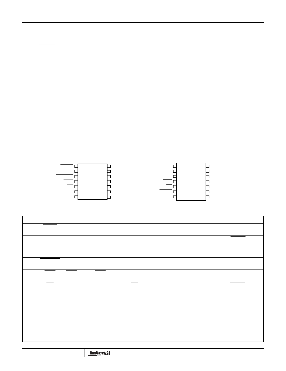
BLOCK DIAGRAM
Standard V
TRIP1
Level Standard V
TRIP2
, Level Suffix
4.6V (+/-1%)
2.9V(+/-1.7%)
-A
4.6V (+/-1%)
2.6V (+/-2%)
-B
2.9V(+/-1.7%)
1.6V (+/-3%)
-C
See "Ordering Information" for more details
For Custom Settings, call Intersil.
V2FAIL
WDO
MR
LOWLINE
RESET
RESET
X40020
X40021
+
-
V2 Monitor
Logic
V
TRIP2
Fault Detection
Register
Status
Register
Data
Register
Command
Decode Test
& Control
Logic
Power-on,
Manual Reset
Low Voltage
Reset
Generation
V
CC
Monitor
Logic
V2MON
SDA
WP
SCL
V
CC
(V1MON)
Watchdog
and
Reset Logic
System
Switch
Battery
V
BATT
V
OUT
BATT-ON
+
-
V
TRIP1
V
OUT
V
OUT
V
OUT
Data Sheet
March 28, 2005
2
FN8112.0
March 28, 2005
Low V
CC
detection circuitry protects the user's system
from low voltage conditions, resetting the system
when V
CC
falls below the minimum V
TRIP1
point.
RESET/RESET is active until V
CC
returns to proper
operating level and stabilizes. A second voltage moni-
tor circuit tracks the unregulated supply to provide a
power fail warning or monitors different power supply
voltage. Three common low voltage combinations are
available. However, Intersil's unique circuits allows the
threshold for either voltage monitor to be repro-
grammed to meet specific system level requirements
or to fine-tune the threshold for applications requiring
higher precision.
A manual reset input provides debounce circuitry for
minimum reset component count.
A battery switch circuit compares V
CC
with V
BATT
input
and connects V
OUT
to whichever is higher. This pro-
vides voltage to external SRAM or other circuits in the
event of main power failure. The X40020/21 can drive
50mA from V
CC
to 250µA from V
BATT
. The device only
switches to V
BATT
when V
CC
drops below the low V
CC
voltage threshold and V
BATT
.
The Watchdog Timer provides an independent protec-
tion mechanism for microcontrollers. When the micro-
controller fails to restart a timer within a selectable
time out interval, the device activates the WDO signal.
The user selects the interval from three preset values.
Once selected, the interval does not change, even
after cycling the power.
The device features an 2-wire interface and software
protocol allowing operation on a two-wire bus.
The device utilizes Intersil's proprietary Direct Write
TM
cell, providing a minimum endurance of 100,000
cycles and a minimum data retention of 100 years.
PIN CONFIGURATION
V
BATT
V
SS
V
CC
SDA
SCL
3
2
4
1
12
13
11
14
LOWLINE
WDO
RESET
7
6
5
8
9
10
V2MON
MR
WP
3
2
4
1
12
13
11
14
7
6
5
8
9
10
V
OUT
BATT-ON
V2FAIL
V
BATT
V
CC
SDA
SCL
WP
V
OUT
BATT-ON
V
SS
LOWLINE
WDO
RESET
V2MON
MR
V2FAIL
X40020
X40021
14-Pin SOIC, TSSOP
14-Pin SOIC, TSSOP
PIN DESCRIPTION
Pin
Name
Function
1
V2FAIL
V2 Voltage Fail Output. This open drain output goes LOW when V2MON is less than V
TRIP2
and
goes HIGH when V2MON exceeds V
TRIP2
. There is no power-up reset delay circuitry on this pin.
2
V2MON
V2 Voltage Monitor Input. When the V2MON input is less than the V
TRIP2
voltage, V2FAIL goes
LOW. This input can monitor an unregulated power supply with an external resistor divider or can
monitor a second power supply with no external components. Connect V2MON to V
SS
or
V
CC
when
not used.
3
LOWLINE
Early Low V
CC
Detect. This open drain output signal goes LOW when
V
CC
< V
TRIP1
.
When
V
CC
> V
TRIP1
, this pin is pulled high with the use of an external pull up resistor.
4
WDO
WDO Output. WDO is an active LOW, open drain output which goes active whenever the watchdog
timer goes active.
5
MR
Manual Reset Input. Pulling the MR pin LOW initiates a system reset. The RESET/RESET pin will
remain HIGH/LOW until the pin is released and for the t
PURST
thereafter. It has an internal pull up
resistor.
6
RESET/
RESET
RESET Output. (X40021) This open drain pin is an active LOW output which goes LOW whenever
V
CC
falls below V
TRIP1
voltage or if manual reset is asserted. This output stays active for the pro-
grammed time period (t
PURST
) on power-up. It will also stay active until manual reset is released and
for t
PURST
thereafter.
RESET Output. (X40020) This pin is an active HIGH open drain output which goes HIGH whenever
V
CC
falls below V
TRIP1
voltage or if manual reset is asserted. This output stays active for the pro-
grammed time period (t
PURST
) on power-up. It will also stay active until manual reset is released and
for t
PURST
thereafter.
X40020, 40021
3
FN8112.0
March 28, 2005
7
V
SS
Ground
8
SDA
Serial Data. SDA is a bidirectional pin used to transfer data into and out of the device. It has an open
drain output and may be wire ORed with other open drain or open collector outputs. This pin requires
a pull up resistor and the input buffer is always active (not gated).
Watchdog Input. A HIGH to LOW transition on the SDA (while SCL is toggled from HIGH to LOW
and followed by a stop condition) restarts the Watchdog timer. The absence of this transition within
the watchdog time out period results in WDO going active.
9
SCL
Serial Clock. The Serial Clock controls the serial bus timing for data input and output.
10
WP
Write Protect. WP HIGH prevents writes to any location in the device (including all the registers). It
has an internal pull down resistor. (>10M
typical)
11
V
BATT
Battery Supply Voltage. This input provides a backup supply in the event of a failure of the
primary V
CC
voltage. The V
BATT
voltage typically provides the supply voltage necessary to
maintain the contents of SRAM and also powers the internal logic to "stay awake." If the battery is not
used, connect V
BATT
to ground.
12
V
OUT
Output Voltage. (V)
V
OUT
= V
CC
if V
CC
> V
TRIP1
.
IF V
CC
< V
TRIP1
then V
OUT
= V
CC
if V
CC
> V
BATT
+ 0.03V
else V
OUT
= V
BATT
(ie if V
CC
< V
BATT
≠ 0.03V)
Note: There is hysteresis around V
BATT
± 0.03V point to avoid oscillation at or near the
switchover voltage. A capacitance of 0.1µF must be connected to V
OUT
to ensure stability.
13
BATT-ON
Battery On. This CMOS output goes HIGH when the V
OUT
switches to V
BATT
and goes LOW when
V
OUT
switches to V
CC
. It is used to drive an external PNP pass transistor when V
CC
= V
OUT
and current
requirements are greater than 50mA.
The purpose of this output is to drive an external transistor to get higher operating currents when the
V
CC
supply is fully functional. In the event of a V
CC
failure, the battery voltage is applied to the V
OUT
pin and the external transistor is turned off. In this "backup condition," the battery only needs to supply
enough voltage and current to keep SRAM devices from losing their data≠there is no communication
at this time.
14
V
CC
Supply Voltage
PIN DESCRIPTION
(Continued)
Pin
Name
Function
X40020, 40021
4
FN8112.0
March 28, 2005
PRINCIPLES OF OPERATION
Power-on Reset
Applying power to the X40020/21 activates a Power-
on Reset Circuit that pulls the RESET/RESET pins
active. This signal provides several benefits.
≠ It prevents the system microprocessor from starting
to operate with insufficient voltage.
≠ It prevents the processor from operating prior to sta-
bilization of the oscillator.
≠ It allows time for an FPGA to download its configura-
tion prior to initialization of the circuit.
≠ It prevents communication to the EEPROM, greatly
reducing the likelihood of data corruption on power-up.
When V
CC
exceeds the device V
TRIP1
threshold value
for t
PURST
(selectable) the circuit releases the RESET
(X40021) and RESET (X40020) pin allowing the system
to begin operation.
Figure 1. Connecting a Manual Reset Push-Button
Manual Reset
By connecting a push-button directly from MR to
ground, the designer adds manual system reset capa-
bility. The MR pin is LOW while the push-button is
closed and RESET/RESET pin remains LOW for
t
PURST
or till the push-button is released and for t
PURST
thereafter. A weak pull up resistor is connected to the
MR pin.
Low Voltage V1 Monitoring
During operation, the X40020/21 monitors the V
CC
level and asserts RESET if supply voltage falls below
a preset minimum V
TRIP1
. The RESET signal prevents
the microprocessor from operating in a power fail or
brownout condition. The V1FAIL signal remains active
until the voltage drops below 1V. It also remains active
until V
CC
returns and exceeds V
TRIP1
for
t
PURST
.
Low Voltage V2 Monitoring
The X40020/21 also monitors a second voltage level and
asserts V2FAIL if the voltage falls below a preset mini-
mum V
TRIP2
. The V2FAIL signal is either ORed with
RESET to prevent the microprocessor from operating in
a power fail or brownout condition or used to interrupt the
microprocessor with notification of an impending power
failure. The V2FAIL signal remains active until the V
CC
drops below 1V (V
CC
falling). It also remains active until
V2MON returns and exceeds V
TRIP2
.
V2MON voltage monitor is powered by V
OUT.
If V
CC
and V
BATT
go away, V2MON cannot be monitored.
Figure 2. Two Uses of Multiple Voltage Monitoring
WATCHDOG TIMER
The Watchdog Timer circuit monitors the microprocessor
activity by monitoring the SDA and SCL pins. A standard
read or write sequence to any slave address byte
restarts the watchdog timer and prevents the WDO sig-
nal to go active. A minimum sequence to reset the
watchdog timer requires four microprocessor instructions
namely, a Start, Clock Low, Clock High and Stop. The
state of two nonvolatile control bits in the Status Register
determine the watchdog timer period. The microproces-
sor can change these watchdog bits by writing to the
X40020/21 control register (also refer to page 21).
MR
System
Reset
Manual
Reset
X40020
RESET
Unreg.
Supply
V
CC
5V
Reg
V2MON
X40020
Resistors selected so 3V appears on V2MON when unregulated
supply reaches 6V.
Unreg.
Supply
V
CC
X40021
RESET
V2FAIL
System
V
OUT
Reset
RESET
V2FAIL
V
OUT
System
Reset
Notice: No external components required to monitor two voltages.
R
R
V2MON
5V
Reg
3V
Reg
X40020, 40021
5
FN8112.0
March 28, 2005
Figure 3. V
TRIPX
Set/Reset Conditions
Figure 4. Watchdog Restart
V1 AND V2 THRESHOLD PROGRAM PROCEDURE
(OPTIONAL)
The X40020/21 is shipped with standard V1 and V2
threshold (V
TRIP1,
V
TRIP2
) voltages. These values will not
change over normal operating and storage conditions.
However, in applications where the standard thresholds
are not exactly right, or if higher precision is needed in
the threshold value, the X40020 trip points may be
adjusted. The procedure is described below, and uses
the application of a high voltage control signal.
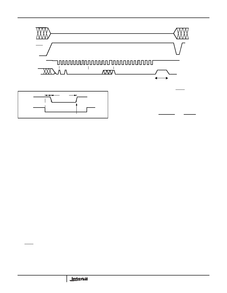
Setting a V
TRIPx
Voltage (x = 1, 2)
There are two procedures used to set the threshold volt-
ages (V
TRIPx
), depending if the threshold voltage to be
stored is higher or lower than the present value. For
example, if the present V
TRIPx
is 2.9 V and the new
V
TRIPx
is 3.2 V, the new voltage can be stored directly
into the V
TRIPx
cell. If however, the new setting is to be
lower than the present setting, then it is necessary to
"reset" the V
TRIPx
voltage before setting the new value.
Setting a Higher V
TRIPx
Voltage (x = 1, 2)
To set a V
TRIPx
threshold to a new voltage which is
higher than the present threshold, the user must apply
the desired V
TRIPx
threshold voltage to the
corresponding input pin (Vcc(V1MON) or V2MON).
Then, a program-ming voltage (Vp) must be applied to
the WDO pin before a START condition is set up on
SDA. Next, issue on the SDA pin the Slave Address A0h,
followed by the Byte Address 01h for V
TRIP1
, and 09h for
V
TRIP2
, and a 00h Data Byte in order to program V
TRIPx
.
The STOP bit following a valid write operation initiates
the programming sequence. Pin WDO must then be
brought LOW to complete the operation.
To check if the V
TRIPX
has been set, set VXMON to a
value slightly greater than V
TRIPX
(that was previously
set). Slowly ramp down VXMON and observe when the
corresponding outputs (LOWLINE and V2FAIL) switch.
The voltage at which this occurs is the V
TRIPX
(actual).
C
ASE
A
Now if the desired V
TRIPX
is greater than the V
TRIPX
(actual), then add the difference between V
TRIPX
(desired) - V
TRIPX
(actual) to the original V
TRIPX
desired.
This is your new V
TRIPX
that should be applied to
VXMON and the whole sequence should be repeated
again (see Figure 5).
C
ASE
B
Now if the V
TRIPX
(actual), is higher than the V
TRIPX
(desired), perform the reset sequence as described in
the next section. The new V
TRIPX
voltage to be applied
to VXMON will now be: V
TRIPX
(desired) - (V
TRIPX
(actual) - V
TRIPX
(desired)).
Note: 1. This operation does not corrupt the memory
array.
2. Set V
CC
= 5V, when V
TRIP2
is being pro-
grammed
Setting a Lower V
TRIPx
Voltage (x = 1, 2)
In order to set V
TRIPx
to a lower voltage than the
present value, then V
TRIPx
must first be "reset" accord-
ing to the procedure described below. Once V
TRIPx
has been "reset", then V
TRIPx
can be set to the desired
voltage using the procedure described in "Setting a
Higher V
TRIPx
Voltage".
V
CC
/V2MON
V
TRIPX
V
P
t
WC
A0h
0
7
7
0
7
0
SCL
WDO
SDA
(X = 1, 2)
00h
SCL
SDA
.6µs
1.3µs
WDT Reset
Start
Stop
X40020, 40021

6
FN8112.0
March 28, 2005
Resetting the V
TRIPx
Voltage
To reset a V
TRIPx
voltage, apply the programming volt-
age (Vp) to the WDO pin before a START condition is
set up on SDA. Next, issue on the SDA pin the Slave
Address A0h followed by the Byte Address 03h for
V
TRIP1
and 0Bh for V
TRIP2
, followed by 00h for the Data
Byte in order to reset V
TRIPx
. The STOP bit following a
valid write operation initiates the programming
sequence. Pin WDO must then be brought LOW to
complete the operation.
After being reset, the value of V
TRIPx
becomes a nominal
value of 1.7V or lesser.
Note: This operation does not corrupt the registers.
System Battery Switch
As long as V
CC
exceeds the low voltage detect thresh-
old V
TRIP
, V
OUT
is connected to V
CC
through a 5
(typi-
cal) switch. When the V
CC
has fallen below V1
TRIP
,
then V
CC
is applied to V
OUT
if V
CC
is or equal to or
greater than V
BATT
- 0.03V. When V
CC
drops to less
than V
BATT
- 0.03V, then V
OUT
is connected to V
BATT
through an 80
(typical) switch. V
OUT
typically supplies
the system static RAM voltage, so the switchover circuit
operates to protect the contents of the static RAM dur-
ing a power failure. Typically, when V
CC
has failed, the
SRAMs go into a lower power state and draw much less
current than in their active mode. When V
CC
returns,
V
OUT
switches back to V
CC
when V
CC
exceeds V
BATT
+
0.03V. There is a 60mV hysteresis around this battery
switch threshold to prevent oscillations between sup-
plies.
While V
CC
is connected to V
OUT
the BATT-ON pin is
pulled LOW. The signal can drive an external PNP tran-
sistor to provide additional current to the external circuits
during normal operation.
Operation
The device is in normal operation with V
CC
as long as
V
CC
> V
TRIP1
. It switches to the battery backup mode
when V
CC
goes away.
Control Register
The Control Register provides the user a mechanism for
changing the Block Lock and Watchdog Timer settings.
The Block Lock and Watchdog Timer bits are nonvolatile
and do not change when power is removed.
The Control Register is accessed with a special pream-
ble in the slave byte (1011) and is located at address
1FFh. It can only be modified by performing a byte write
operation directly to the address of the register and only
one data byte is allowed for each register write operation.
Prior to writing to the Control Register, the WEL and
RWEL bits must be set using a two step process, with
the whole sequence requiring 3 steps. See "Writing to
the Control Registers" on page 8.
The user must issue a stop, after sending this byte to the
register, to initiate the nonvolatile cycle that stores WD1,
WD0, PUP1, and PUP0. The X40020 will not acknowl-
edge any data bytes written after the first byte is entered.
The state of the Control Register can be read at any time
by performing a random read at address 01Fh, using the
special preamble. Only one byte is read by each register
read operation. The master should supply a stop condi-
tion to be consistent with the bus protocol, but a stop is
not required to end this operation.
RWEL: Register Write Enable Latch (Volatile)
The RWEL bit must be set to "1" prior to a write to the
Control Register.
Figure 5. Sample V
TRIP
Reset Circuit
Condition
Mode of Operation
V
CC
> V
TRIP1
Normal Operation
V
CC
> V
TRIP1
&
V
BATT
= 0
Normal Operation without battery
backup capability
0
V
CC
V
TRIP1
and V
CC
< V
BATT
Battery Backup mode; RESET
signal is asserted. No communica-
tion to the device is allowed.
7
6
5
4
3
2
1
0
PUP1 WD1 WD0
0
0
RWEL WEL PUP0
1
6
2
7
14
13
9
8
X40020
V
TRIP1
Adj.
V
P
RESET
4.7K
SDA
SCL
µC
Adjust
Run
V2FAIL
V
TRIP2
Adj.
X40020, 40021
7
FN8112.0
March 28, 2005
Figure 6. V
TRIPX
Set/Reset Sequence (X = 1, 2)
WEL: Write Enable Latch (Volatile)
The WEL bit controls the access to the memory and to
the Register during a write operation. This bit is a vola-
tile latch that powers up in the LOW (disabled) state.
While the WEL bit is LOW, writes to any address,
including any control registers will be ignored (no
acknowledge will be issued after the Data Byte). The
WEL bit is set by writing a "1" to the WEL bit and
zeroes to the other bits of the control register.
Once set, WEL remains set until either it is reset to 0
(by writing a "0" to the WEL bit and zeroes to the other
bits of the control register) or until the part powers up
again. Writes to the WEL bit do not cause a high volt-
age write cycle, so the device is ready for the next
operation immediately after the stop condition.
V
TRIPX
Programming
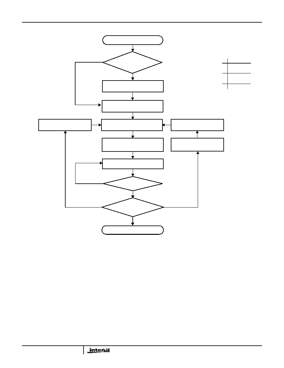
Apply V
CC
and Voltage
Decrease V
X
Actual V
TRIPX -
Desired V
TRIPX
DONE
Set Higher V
X
Sequence
Error < MDE
≠
| Error | < | MDE |
YES
NO
Error > MDE
+
> Desired V
TRIPX
to V
X
Desired
Present Value
V
TRIPX
<
Execute
No
YES
Execute
V
TRIPX
Reset Sequence
Set V
X
= desired V
TRIPX
New V
X
applied =
Old V
X
applied + | Error |
New V
X
applied =
Old V
X
applied - | Error |
Execute Reset V
TRIPX
Sequence
Output Switches?
Note: X = 1, 2
Let: MDE = Maximum Desired Error
Vx = V
CC
, VxMON
MDE
+
Desired Value
MDE
≠
Acceptable
Error Range
Error = Actual - Desired
X40020, 40021

8
FN8112.0
March 28, 2005
BP: Block Protect Bit (Nonvolatile)
The Block Protect Bits BP determines which blocks of
the array are write protected. A write to a protected
block of memory is ignored. The block protect bit will
prevent write operations to half the array segment.
PUP1, PUP0: Power-up Bits (Nonvolatile)
The Power-up bits, PUP1 and PUP0, determine the
t
PURST
time delay. The nominal power-up times are
shown in the following table.
WD1, WD0: Watchdog Timer Bits
The bits WD1 and WD0 control the period of the
Watchdog Timer. The options are shown below.
Writing to the Control Registers
Changing any of the nonvolatile bits of the control and
trickle registers requires the following steps:
≠ Write a 02H to the Control Register to set the Write
Enable Latch (WEL). This is a volatile operation, so
there is no delay after the write. (Operation pre-
ceded by a start and ended with a stop).
≠ Write a 06H to the Control Register to set the
Register Write Enable Latch (RWEL) and the WEL
bit. This is also a volatile cycle. The zeros in the data
byte are required. (Operation proceeded by a start
and ended with a stop).
≠ Write a one byte value to the Control Register that
has all the control bits set to the desired state. The
Control register can be represented as qxy0 001r in
binary, where xy are the WD bits, and qr are the
power-up bits. This operation proceeded by a start
and ended with a stop bit. Since this is a nonvolatile
write cycle it will take up to 10ms to complete. The
RWEL bit is reset by this cycle and the sequence
must be repeated to change the nonvolatile bits
again. If bit 2 is set to `1' in this third step (qxy0 011r)
then the RWEL bit is set, but the WD1, WD0, PUP1,
and PUP0, bits remain unchanged. Writing a second
byte to the control register is not allowed. Doing so
aborts the write operation and returns a NACK.
≠ A read operation occurring between any of the previ-
ous operations will not interrupt the register write
operation.
≠ The RWEL bit cannot be reset without writing to the
nonvolatile control bits in the control register, power
cycling the device or attempting a write to a write
protected block.
To illustrate, a sequence of writes to the device con-
sisting of [02H, 06H, 02H] will reset all of the nonvola-
tile bits in the Control Register to 0. A sequence of
[02H, 06H, 06H] will leave the nonvolatile bits
unchanged and the RWEL bit remains set.
Note: 1. t
PURST
is set to 200ms as factory default.
2. Watchdog timer bits are shipped disabled.
Fault Detection Register (FDR)
The Fault Detection Register provides the user the
status of what causes the system reset active. The
Manual Reset Fail, Watchdog Timer Fail and Three
Low Voltage Fail bits are volatile.
The FDR is accessed with a special preamble in the
slave byte (1011) and is located at address 0FFh. It
can only be modified by performing a byte write opera-
tion directly to the address of the register and only one
data byte is allowed for each register write operation.
There is no need to set the WEL or RWEL in the con-
trol register to access this fault detection register.
BP
Protected Addresses
(Size)
Memory
Array Lock
0
None
None
1
100h - 1FFh (256 bytes)
Upper Half of
Memory Array
PUP1 PUP0
Power-on Reset Delay (
t
PURST
)
0
0
50ms
0
1
200ms (default)
1
0
400ms
1
1
800ms
WD1
WD0
Watchdog Time Out Period
0
0
1.4 seconds
0
1
200 milliseconds
1
0
25 milliseconds
1
1
disabled (factory default)
7
6
5
4
3
2
1
0
LV1F LV2F
0
WDF MRF
0
0
0
X40020, 40021
9
FN8112.0
March 28, 2005
Figure 7. Valid Data Changes on the SDA Bus
At power-up, the Fault Detection Register is defaulted
to all "0". The system needs to initialize this register to
all "1" before the actual monitoring take place. In the
event of any one of the monitored sources failed. The
corresponding bits in the register will change from a
"1" to a "0" to indicate the failure. At this moment, the
system should perform a read to the register and
noted the cause of the reset. After reading the register
the system should reset the register back to all "1"
again. The state of the Fault Detection Register can be
read at any time by performing a random read at
address 0FFh, using the special preamble.
The FDR can be read by performing a random read at
0FFh address of the register at any time. Only one
byte of data is read by the register read operation.
MRF, Manual Reset Fail Bit (Volatile)
The MRF bit will set to "0" when Manual Reset input
goes active.
WDF, Watchdog Timer Fail Bit (Volatile)
The WDF bit will set to "0" when WDO goes active.
LV1F, Low V
CC
Reset Fail Bit (Volatile)
The LV1F bit will be set to "0" when V
CC
(V1MON)
falls below V
TRIP1
.
LV2F, Low V2MON Reset Fail Bit (Volatile)
The LV2F bit will be set to "0" when V2MON falls
below V
TRIP2
.
Interface Conventions
The device supports a bidirectional bus oriented proto-
col. The protocol defines any device that sends data
onto the bus as a transmitter, and the receiving device
as the receiver. The device controlling the transfer is
called the master and the device being controlled is
called the slave. The master always initiates data
transfers, and provides the clock for both transmit and
receive operations. Therefore, the devices in this fam-
ily operate as slaves in all applications.
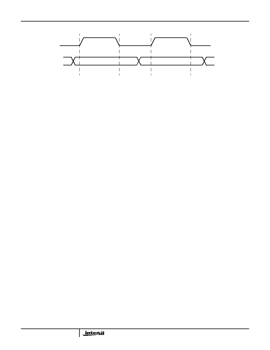
Serial Clock and Data
Data states on the SDA line can change only during
SCL LOW. SDA state changes during SCL HIGH are
reserved for indicating start and stop conditions. See
Figure 7.
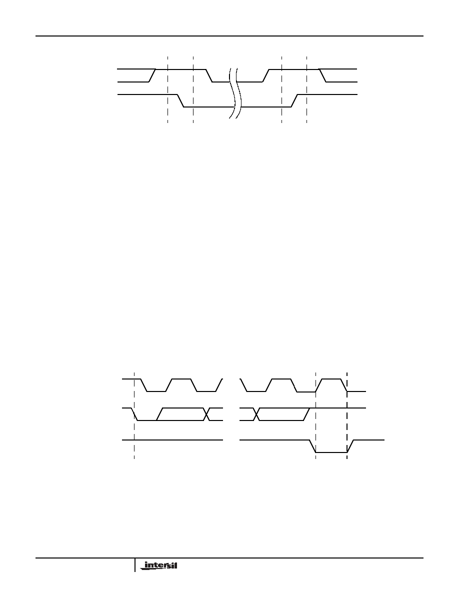
Serial Start Condition
All commands are preceded by the start condition,
which is a HIGH to LOW transition of SDA when SCL
is HIGH. The device continuously monitors the SDA
and SCL lines for the start condition and will not
respond to any command until this condition has been
met. See Figure 8.
Serial Stop Condition
All communications must be terminated by a stop con-
dition, which is a LOW to HIGH transition of SDA when
SCL is HIGH. The stop condition is also used to place
the device into the Standby power mode after a read
sequence. A stop condition can only be issued after the
transmitting device has released the bus. See Figure 8.
SCL
SDA
Data Stable
Data Change
Data Stable
X40020, 40021
10
FN8112.0
March 28, 2005
Figure 8. Valid Start and Stop Conditions
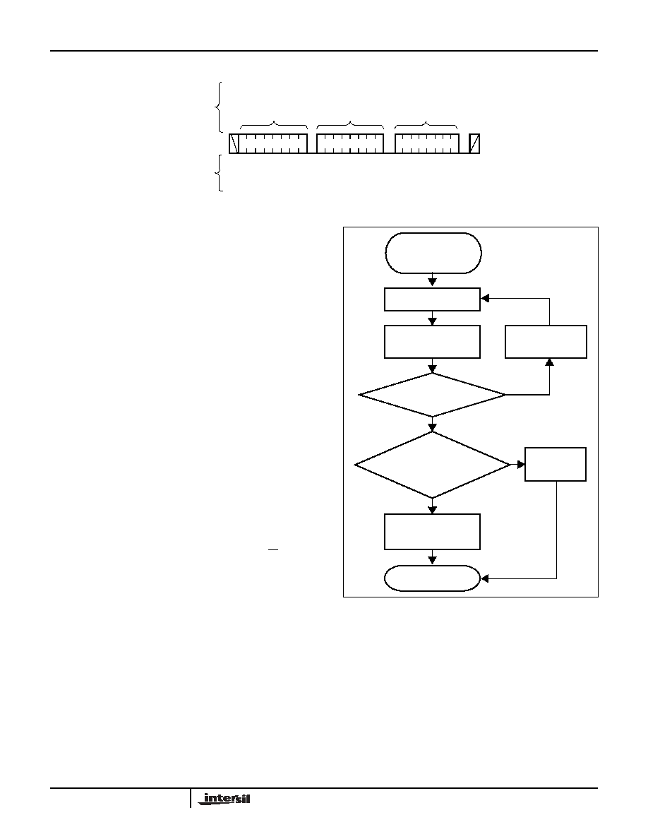
Serial Acknowledge
Acknowledge is a software convention used to indi-
cate successful data transfer. The transmitting device,
either master or slave, will release the bus after trans-
mitting eight bits. During the ninth clock cycle, the
receiver will pull the SDA line LOW to acknowledge
that it received the eight bits of data. See Figure 9.
The device will respond with an acknowledge after
recognition of a start condition and if the correct
Device Identifier and Select bits are contained in the
Slave Address Byte. If a write operation is selected,
the device will respond with an acknowledge after the
receipt of each subsequent eight bit word. The device
will acknowledge all incoming data and address bytes,
except for the Slave Address Byte when the Device
Identifier and/or Select bits are incorrect.
In the read mode, the device will transmit eight bits of
data, release the SDA line, then monitor the line for an
acknowledge. If an acknowledge is detected and no
stop condition is generated by the master, the device
will continue to transmit data. The device will terminate
further data transmissions if an acknowledge is not
detected. The master must then issue a stop condition
to return the device to Standby mode and place the
device into a known state.
Serial Write Operations
Byte Write
For a write operation, the device requires the Slave
Address Byte and a Word Address Byte. This gives
the master access to any one of the words in the
array. After receipt of the Word Address Byte, the
device responds with an acknowledge, and awaits the
next eight bits of data. After receiving the 8 bits of the
Data Byte, the device again responds with an
acknowledge. The master then terminates the transfer
by generating a stop condition, at which time the
device begins the internal write cycle to the nonvolatile
memory. During this internal write cycle, the device
inputs are disabled, so the device will not respond to any
requests from the master. The SDA output is at high
impedance.
Figure 9. Acknowledge Response From Receiver
SCL
SDA
Start
Stop
Data Output
from
Data Output
from Receiver
8
1
9
Start
Acknowledge
SCL from
Master
X40020, 40021
11
FN8112.0
March 28, 2005
Figure 10. Byte Write Sequence
Stops and Write Modes
Stop conditions that terminate write operations must
be sent by the master after sending at least 1 full data
byte plus the subsequent ACK signal. If a stop is
issued in the middle of a data byte, or before 1 full
data byte plus its associated ACK is sent, then the
device will reset itself without performing the write. The
contents of the array will not be effected.
Acknowledge Polling
The disabling of the inputs during high voltage cycles
can be used to take advantage of the typical 5ms write
cycle time. Once the stop condition is issued to indi-
cate the end of the master's byte load operation, the
device initiates the internal high voltage cycle.
Acknowledge polling can be initiated immediately. To
do this, the master issues a start condition followed by
the Slave Address Byte for a write or read operation. If
the device is still busy with the high voltage cycle then
no ACK will be returned. If the device has completed
the write operation, an ACK will be returned and the
host can then proceed with the read or write operation.
See Figure 11.
Serial Read Operations
Read operations are initiated in the same manner as
write operations with the exception that the R/W bit of
the Slave Address Byte is set to one.
Figure 11. Acknowledge Polling Sequence
S
t
a
r
t
S
t
o
p
Slave
Address
Byte
Address
Data
A
C
K
A
C
K
A
C
K
SDA Bus
Signals from
the Slave
Signals from
the Master
0
ACK
Returned?
Issue Slave Address
Byte (Read or Write)
Byte Load Completed
by Issuing STOP.
Enter ACK Polling
Issue STOP
Issue START
NO
YES
High Voltage Cycle
Complete. Continue
Command Sequence?
Issue STOP
NO
Continue Normal
Read or Write
Command Sequence
PROCEED
YES
X40020, 40021
12
FN8112.0
March 28, 2005
Read Operation
Prior to issuing the Slave Address Byte with the R/W bit
set to one, the master must first perform a "dummy" write
operation. The master issues the start condition and the
Slave Address Byte, receives an acknowledge, then
issues the Word Address Bytes. After acknowledging
receipts of the Word Address Bytes, the master immedi-
ately issues another start condition and the Slave
Address Byte with the R/W bit set to one. This is followed
by an acknowledge from the device and then by the eight
bit word. The master terminates the read operation by
not responding with an acknowledge and then issuing a
stop condition. See Figure 12 for the address, acknowl-
edge, and data transfer sequence.
SERIAL DEVICE ADDRESSING
Memory Address Map
CR, Control Register, CR7: CR0
Address: 1FF
hex
FDR, Fault DetectionRegister, FDR7: FDR0
Address: 0FF
hex
Slave Address Byte
Following a start condition, the master must output a
Slave Address Byte. This byte consists of several parts:
≠ a device type identifier that is always "1011" when
accessing the control register and fault detection
register.
≠ two bits of "0".
≠ one bit that becomes the MSB of the memory
address X
4
.
≠ last bit of the slave command byte is a R/W bit. The
R/W bit of the Slave Address Byte defines the oper-
ation to be performed. When the R/W bit is a one,
then a read operation is selected. A zero selects a
write operation. See Figure 13.
Figure 12. Read Sequence
0
Slave
Address
Byte
Address
A
C
K
A
C
K
S
t
a
r
t
S
t
o
p
Slave
Address
Data
A
C
K
1
S
t
a
r
t
SDA Bus
Signals from
the Slave
Signals from
the Master
1 0 1
0 0
1
1 1 1 1 1 1 1 1
X40020, 40021
13
FN8112.0
March 28, 2005
Figure 13. Slave Address, Word Address, and Data Bytes
Word Address
The word address is either supplied by the master or
obtained from an internal counter.
Operational Notes
The device powers-up in the following state:
≠ The device is in the low power standby state.
≠ The WEL bit is set to `0'. In this state it is not possi-
ble to write to the device.
≠ SDA pin is the input mode.
≠ RESET/RESET Signal is active for
t
PURST
.
Data Protection
The following circuitry has been included to prevent
inadvertent writes:
≠ The WEL bit must be set to allow write operations.
≠ The proper clock count and bit sequence is required
prior to the stop bit in order to start a nonvolatile
write cycle.
≠ A three step sequence is required before writing into
the Control Register to change Watchdog Timer or
Block Lock settings.
≠ The WP pin, when held HIGH, prevents all writes to
the array and all the Register.
General Purpose Memory
Control Register
Fault Detection Register
1
1
0
0
1
1
0
1
A8 R/W
Word Address
Slave Byte
1
0
1
0
1
1
0
0
0
0
0
0
R/W
R/W
General Purpose Memory
Control Register
Fault Detection Register
A7
1
A6 A5 A4
A1 A0
1
A3 A2
1
1
1
1
1
1
1
1
1
1
1
1
1
1
X40020, 40021
14
FN8112.0
March 28, 2005
ABSOLUTE MAXIMUM RATINGS
Temperature under bias .................... -65∞C to +135∞C
Storage temperature ......................... -65∞C to +150∞C
Voltage on any pin with
respect to V
SS
...................................... -1.0V to +7V
D.C. output current ............................................... 5mA
Lead temperature (soldering, 10 seconds)........ 300∞C
COMMENT
Stresses above those listed under "Absolute Maximum
Ratings" may cause permanent damage to the device.
This is a stress rating only; functional operation of the
device (at these or any other conditions above those
listed in the operational sections of this specification) is
not implied. Exposure to absolute maximum rating con-
ditions for extended periods may affect device reliability.
RECOMMENDED OPERATING CONDITIONS
*See Ordering Info
Temperature
Min.
Max.
Commercial
0∞C
70∞C
Industrial
-40∞C
+85∞C
Version Chip Supply Voltage
Monitored
Voltages*
-A or -B
2.7V to 5.5V
2.6 to 5.5V
-C
2.7V to 5.5V
1.6V to 3.6V
D.C. OPERATING CHARACTERISTICS
(Over the recommended operating conditions unless otherwise specified)
Symbol
Parameter
Min.
Typ.
(5)
Max.
Unit
Test Conditions
I
CC1
(1)
Active Supply Current (
V
CC
) Read
(Excludes I
OUT
)
1.5
mA V
IL
=
V
CC
x 0.1
V
IH
=
V
CC
x 0.9,
f
SCL
= 400kHz
I
CC2
(1)
Active Supply Current (
V
CC
) Write Non
Volatile Memory (Excludes I
OUT
)
3.0
mA
I
SB1
(1)(7)
Standby Current (
V
CC
) AC (WDT off)
6
10
µA
V
IL
=
V
CC
x 0.1
VIH =
V
CC
x 0.9
f
SCL
, f
SDA
= 400kHz
I
SB2
(2)(7)
Standby Current (
V
CC
) DC (WDT on)
25
30
µA
V
SDA
= V
SCL
=
V
CC
Others = GND or
V
CC
I
BATT1
(3)(7
)
V
BATT
Current (Excludes I
OUT
)
0.2
1
µA
V
OUT
=
V
CC
I
BATT2
(7)
V
BATT
Current (Excludes I
OUT
)
(Battery Backup Mode)
0.2
6
µA
V
BATT
=
2.8V
V
OUT
=
Open
V
OUT1
(7)
Output Voltage (V
CC
> V
BATT
+ 0.03V
or V
CC
> V
TRIP1
)
V
CC
-0.05V
V
CC
-0.5V
V
I
OUT
= 5mA V
CC
= (4.5-5.5V)
I
OUT
= 50mA V
CC
= (4.5-5.5V)
V
OUT2
(7)
Output Voltage (V
CC
< V
BATT
- 0.03V
and V
CC
< V
TRIP1
) {Battery Backup}
V
BATT
-0.2
V
I
OUT
= 250µA
V
OLB
Output (BATT-ON) LOW Voltage
0.4
V
I
OL
= 3.0mA (4.5-5.5V)
V
OHB
Output (BATT-ON) HIGH Voltage
V
OUT
-0.8
V
I
OH
= -0.4mA (4.5-5.5V)
V
BSH
(7)
Battery Switch Hysteresis
(V
CC
< V
TRIP1
)
30
-30
mV Power-up
Power-down
I
LI
Input Leakage Current (SCL, MR,WP)
10
µA
V
IL
= GND to
V
CC
I
LO
Output Leakage Current (SDA, V2FAIL,
WDO, RESET)
10
µA
V
SDA
= GND to
V
CC
Device is in Standby
(2)
V
IL
(3)
Input LOW Voltage (SDA, SCL, MR,WP)
-0.5
V
CC
x 0.3
V
V
IH
(3)
Input HIGH Voltage (SDA, SCL, MR,WP)
V
CC
x 0.7
V
CC
+ 0.5
V
X40020, 40021
15
FN8112.0
March 28, 2005
Notes: (1) The device enters the Active state after any start, and remains active until: 9 clock cycles later if the Device Select Bits in the Slave
Address Byte are incorrect; 200ns after a stop ending a read operation; or t
WC
after a stop ending a write operation.
(2) The device goes into Standby: 200ns after any stop, except those that initiate a high voltage write cycle; t
WC
after a stop that initiates a
high voltage cycle; or 9 clock cycles after any start that is not followed by the correct Device Select Bits in the Slave Address Byte.
(3) Negative numbers indicate charging current, positive numbers indicate discharge current.
(4) V
IL
Min. and V
IH
Max. are for reference only and are not tested.
(5) At 25∞C, V
CC
= 3V.
(6) See ordering information for standard programming levels. For custom programming levels, contact factory.
(7) Based on characterization data.
EQUIVALENT INPUT CIRCUIT FOR VxMON (x = 1, 2)
V
HYS
(7)
Schmitt Trigger Input Hysteresis
∑ Fixed input level
∑
V
CC
related level
0.2
.05 x
V
CC
V
V
V
OL
Output LOW Voltage (SDA, RESET/RE-
SET, LOWLINE, V2FAIL, WDO)
0.4
V
I
OL
= 3.0mA (2.7-5.5V)
I
OL
= 1.8mA (2.4-3.6V)
V
CC
Supply
V
TRIP1
(6)
V
CC
Reset Trip Point Voltage Range
2.0
4.75
V
4.55
4.6
4.65
A, B Version
2.85
2.9
2.95
C Version
t
RPDL
(7)
V
TRIP
1
to LOWLINE
5
µS
Second Supply Monitor
V
TRIP2
(6)
V2MON Reset Trip Point Voltage Range
0.9
3.5
V
2.85
2.9
2.95
A Version
2.55
2.6
2.65
B Version
1.55
1.6
1.65
C Version
t
RPD2
(7)
V
TRIP
2
to V2FAIL
5
µS
D.C. OPERATING CHARACTERISTICS
(Continued)
(Over the recommended operating conditions unless otherwise specified)
Symbol
Parameter
Min.
Typ.
(5)
Max.
Unit
Test Conditions
+
≠
V
REF
t
RPDX
= 5µs worst case
Output
VxMON
R
C
V = 100mV
V
V
REF
X40020, 40021
16
FN8112.0
March 28, 2005
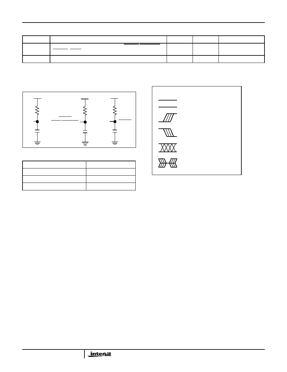
CAPACITANCE
Note:
(1) This parameter is not 100% tested.
EQUIVALENT A.C. OUTPUT LOAD CIRCUIT FOR
V
CC
= 5V
A.C. TEST CONDITIONS)
SYMBOL TABLE
Symbol
Parameter
Max.
Unit
Test Conditions
C
OUT
(1)
Output Capacitance (SDA, RESET, RESET/LOWLINE,
V2FAIL, WDO)
8
pF
V
OUT
= 0V
C
IN
(1)
Input Capacitance (SCL, WP)
6
pF
V
IN
= 0V
Input pulse levels
V
CC
x 0.1 to
V
CC
x 0.9
Input rise and fall times
10ns
Input and output timing levels
V
CC
x 0.5
Output load
Standard output load
5V
SDA
30pF
V2MON
4.6k
RESET
30pF
2.06k
V2FAIL
V
OUT
4.6k
30pF
WDO/LOWLINE
Must be
steady
Will be
steady
May change
from LOW
Will change
from LOW
to HIGH
May change
from HIGH
to LOW
Will change
from HIGH
to LOW
Don't Care:
Changes
Allowed
Changing:
State Not
Known
N/A
Center Line
is High
Impedance
WAVEFORM
INPUTS
OUTPUTS
X40020, 40021

17
FN8112.0
March 28, 2005
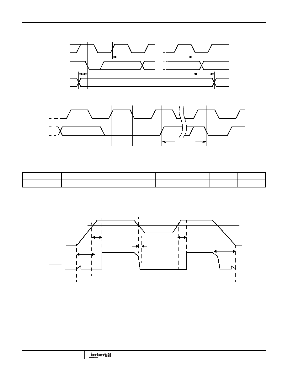
A.C. CHARACTERISTICS
Note:
(1) Cb = total capacitance of one bus line in pF.
TIMING DIAGRAMS
Bus Timing
Symbol
Parameter
400kHz
Unit
Min.
Max.
f
SCL
SCL Clock Frequency
400
kHz
t
IN
Pulse width Suppression Time at inputs
50
ns
t
AA
SCL LOW to SDA Data Out Valid
0.1
0.9
µs
t
BUF
Time the bus free before start of new transmission
1.3
µs
t
LOW
Clock LOW Time
1.3
µs
t
HIGH
Clock HIGH Time
0.6
µs
t
SU:STA
Start Condition Setup Time
0.6
µs
t
HD:STA
Start Condition Hold Time
0.6
µs
t
SU:DAT
Data In Setup Time
100
ns
t
HD:DAT
Data In Hold Time
0
µs
t
SU:STO
Stop Condition Setup Time
0.6
µs
t
DH
Data Output Hold Time
50
ns
t
R
SDA and SCL Rise Time
20 +.1Cb
(1)
300
ns
t
F
SDA and SCL Fall Time
20 +.1Cb
(1)
300
ns
t
SU:WP
WP Setup Time
0.6
µs
t
HD:WP
WP Hold Time
0
µs
Cb
Capacitive load for each bus line
400
pF
t
SU:STO
t
HIGH
t
SU:STA
t
HD:STA
t
HD:DAT
t
SU:DAT
SCL
SDA IN
SDA OUT
t
F
t
LOW
t
BUF
t
R
t
DH
t
AA
X40020, 40021
18
FN8112.0
March 28, 2005
WP Pin Timing
Write Cycle Timing
Nonvolatile Write Cycle Timing
Note:
(1) t
WC
is the time from a valid stop condition at the end of a write sequence to the end of the self-timed internal nonvolatile write cycle. It is
the minimum cycle time to be allowed for any nonvolatile write by the user, unless Acknowledge Polling is used.
Power Fail Timings
Symbol
Parameter
Min.
Typ.
(1)
Max.
Unit
t
WC
(1)
Write Cycle Time
5
10
ms
t
HD:WP
SCL
SDA IN
WP
t
SU:WP
Clk 1
Clk 9
Slave Address Byte
START
SCL
SDA
t
WC
8
th
Bit of Last Byte
ACK
Stop
Condition
Start
Condition
V2MON
V2FAIL
t
R
t
F
t
RPDX
V
RVALID
LOWLINE or
V
CC
or
V
TRIPX
t
RPDX
t
RPDX
t
RPDL
t
RPDL
t
RPDL
X = 1, 2
X40020, 40021
19
FN8112.0
March 28, 2005
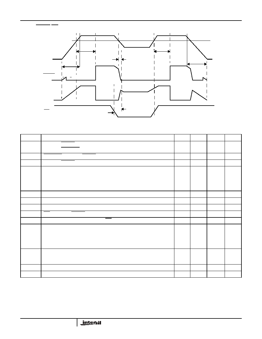
RESET/RESET/MR Timings
LOW VOLTAGE AND WATCHDOG TIMINGS PARAMETERS (@25∞C, VCC = 5V)
Note:
(1) Based on characterization data.
Symbol
Parameters
Min.
Typ.
Max.
Unit
t
RPD1
(1)
t
RPDL
V
TRIP1
to RESET/RESET (Power-down only)
V
TRIP1
to LOWLINE
5
µs
t
LR
(1)
LOWLINE to RESET/RESET delay (Power-down only) [= t
RPD1
-t
RPDL
]
500
ns
t
RPD2
(1)
V
TRIP2
to V2FAIL
5
µs
t
PURST
Power-on Reset delay:
PUP1 = 0, PUP0 = 0
PUP1 = 0, PUP0 = 1 (Factory default)
PUP1 = 1, PUP0 = 0
PUP1 = 1, PUP0 = 1
50
(1)
200
400
(1)
800
(1)
ms
ms
ms
ms
t
F
V
CC,
V2MON
Fall Time
20
mV
/
µs
t
R
V
CC,
V2MON
Rise Time
20
mV
/
µs
V
RVALID
Reset Valid V
CC
1
V
t
MD
(1)
MR to RESET/ RESET delay (activation only)
500
ns
t
in1
Pulse width Suppression Time for MR 50
ns
t
WDO
Watchdog Timer Period:
WD1 = 0, WD0 = 0
WD1 = 0, WD0 = 1
WD1 = 1, WD0 = 0
WD1 = 1, WD0 = 1 (factory default)
1.4
(1)
200
(1)
25
OFF
s
ms
ms
t
RST1
Watchdog Reset Time Out Delay
WD1 = 0, WD0 = 0
WD1 = 0, WD0 = 1
100
200
300
ms
t
RST2
Watchdog Reset Time Out Delay WD1=1, WD0=0
12.5
25
37.5
ms
t
RSP
Watchdog timer restart pulse width
1
µs
V
CC
V
TRIP1
RESET
RESET
t
PURST
t
PURST
t
R
t
F
t
RPD1
V
RVALID
MR
t
MD
X40020, 40021
20
FN8112.0
March 28, 2005
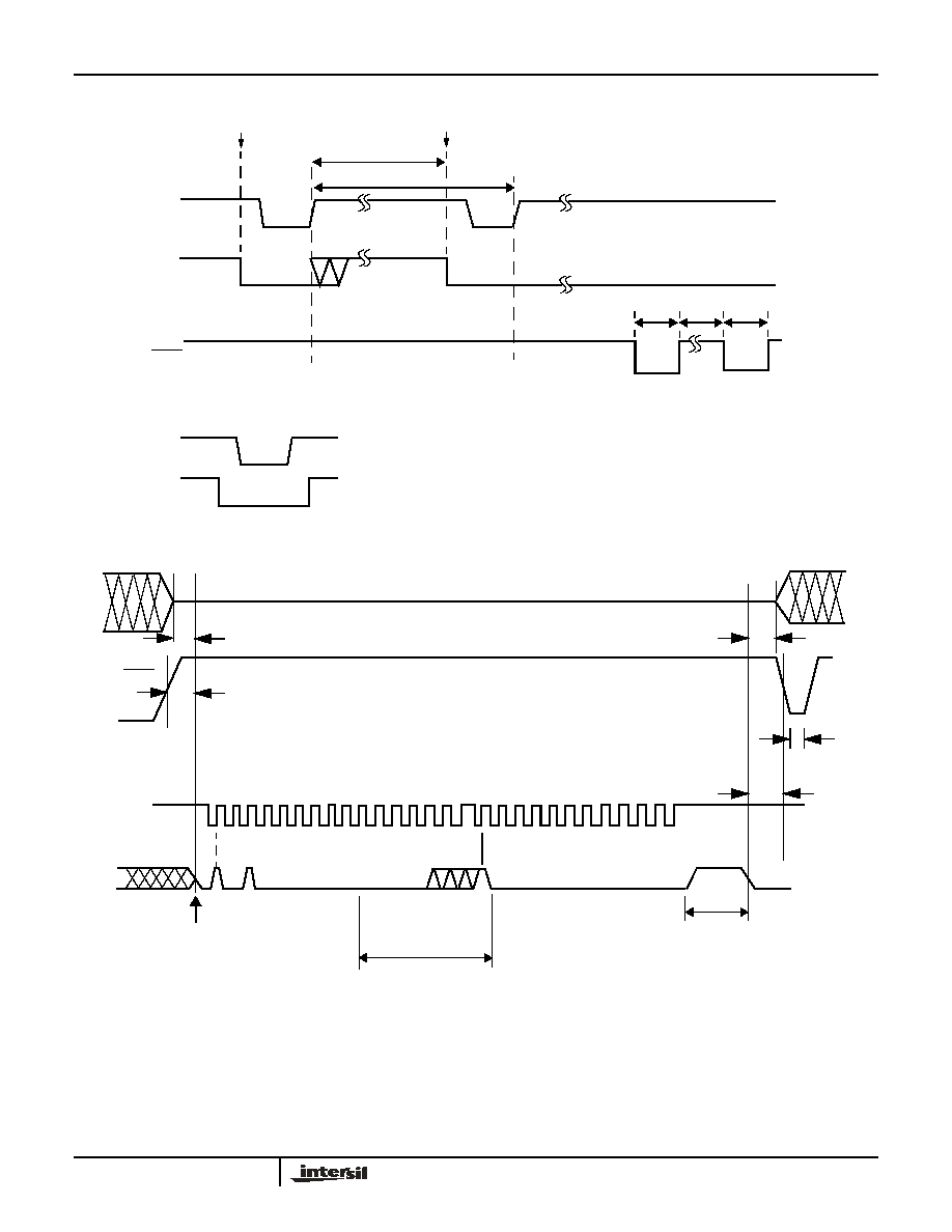
Watchdog Time Out For 2-Wire Interface
V
TRIPX
Set/Reset Conditions
< t
WDO
t
RST
WDO
SDA
Start
t
WDO
t
RST
SCL
Start
t
RSP
WDT
Restart
Start
SDA
SCL
Minimum Sequence to Reset WDT
Clockin (0 or 1)
SCL
SDA
V
CC
/V2MON
(V
TRIPX
)
WDO
t
TSU
t
THD
t
VPH
t
VPS
V
P
t
WC
t
VPO
A0h
0
7
7
0
7
sets V
TRIP1
sets V
TRIP2
*01h
*09h
*03h
*0Bh resets V
TRIP2
resets V
TRIP1
0
Start
* all others reserved
00h
*
X40020, 40021

21
FN8112.0
March 28, 2005
V
TRIP1
, V
TRIP2
Programming Specifications: V
CC
= 2.0-5.5V; Temperature = 25∞C
Parameter
Description
Min.
Max.
Unit
t
VPS
WDO Program Voltage Setup time
10
µs
t
VPH
WDO Program Voltage Hold time
10
µs
t
TSU
V
TRIPX
Level Setup time
10
µs
t
THD
V
TRIPX
Level Hold (stable) time
10
µs
t
WC
V
TRIPX
Program Cycle
10
ms
t
VPO
Program Voltage Off time before next cycle
1
ms
V
P
Programming Voltage
15
18
V
V
TRAN1
V
TRIP1
Set Voltage Range
2.0
4.75
V
V
TRAN2
V
TRIP2
Set Voltage Range
0.9
3.5
V
V
tv
V
TRIPX
Set Voltage variation after programming (0-75∞C).
-25
+25
mV
t
VPS
WDO Program Voltage Setup time
10
µs
V
TRIPX
programming parameters are periodically sampled and are not 100% tested.
X40020, 40021
22
FN8112.0
March 28, 2005
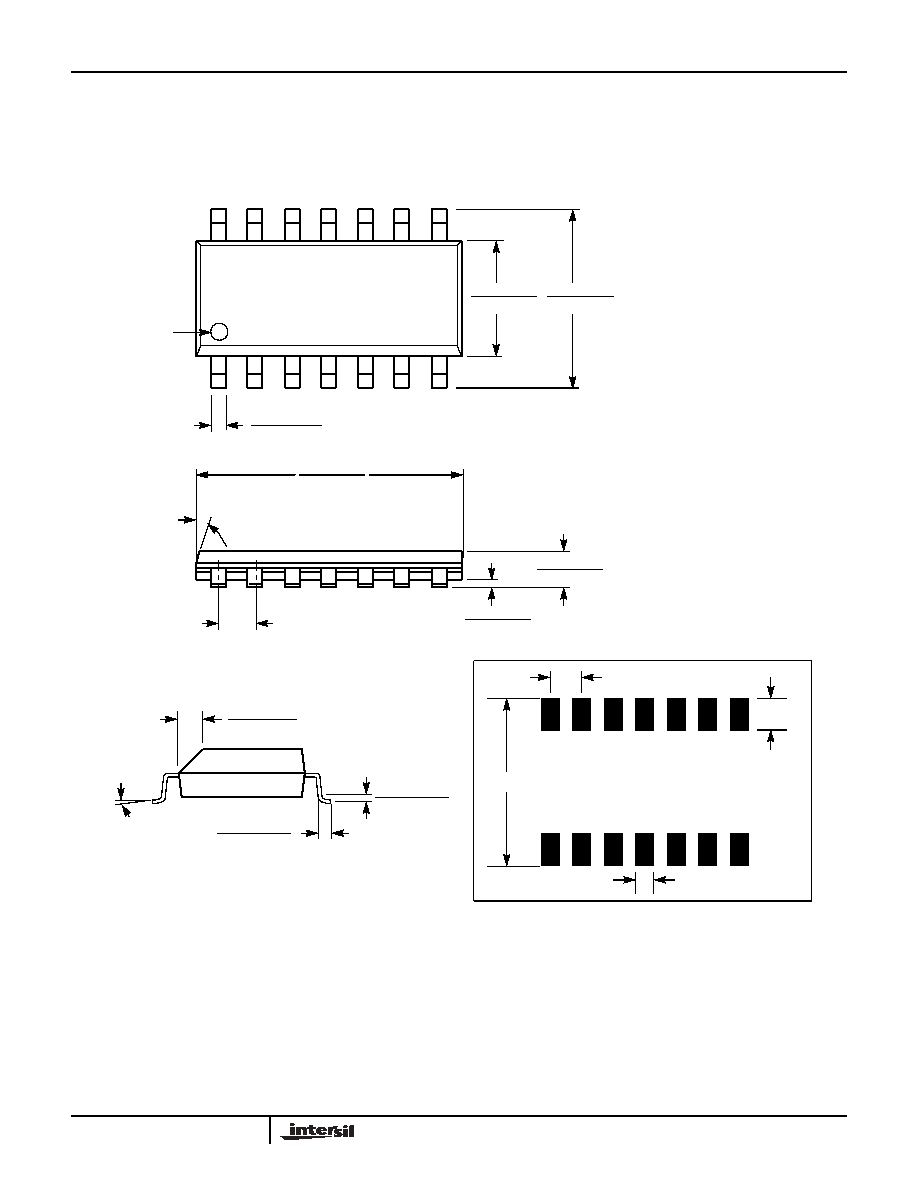
PACKAGING INFORMATION
0.150 (3.80)
0.158 (4.00)
0.228 (5.80)
0.244 (6.20)
0.014 (0.35)
0.020 (0.51)
Pin 1
Pin 1 Index
0.050 (1.27)
0.336 (8.55)
0.345 (8.75)
0.004 (0.10)
0.010 (0.25)
0.053 (1.35)
0.069 (1.75)
(4X) 7∞
14-Lead Plastic Small Outline Gullwing Package Type S
NOTE: ALL DIMENSIONS IN INCHES (IN PARENTHESES IN MILLIMETERS)
0.250"
0.050"Typical
0.050"Typical
0.030"Typical
14 Places
FOOTPRINT
0.010 (0.25)
0.020 (0.50)
0.016 (0.410)
0.037 (0.937)
0.0075 (0.19)
0.010 (0.25)
0∞ - 8∞
X 45∞
X40020, 40021
23
FN8112.0
March 28, 2005
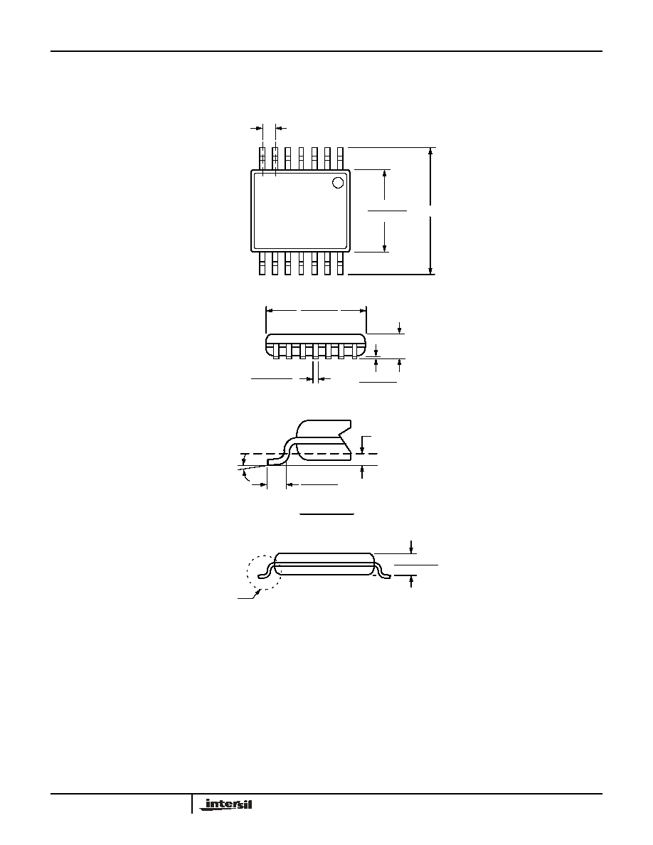
PACKAGING INFORMATION
NOTE: ALL DIMENSIONS IN INCHES (IN PARENTHESES IN MILLIMETERS)
14-Lead Plastic, TSSOP, Package Type V
See Detail "A"
.031 (.80)
.041 (1.05)
.169 (4.3)
.177 (4.5) .252 (6.4) BSC
.025 (.65) BSC
.193 (4.9)
.200 (5.1)
.002 (.05)
.006 (.15)
.047 (1.20)
.0075 (.19)
.0118 (.30)
0∞ - 8∞
.010 (.25)
.019 (.50)
.029 (.75)
Gage Plane
Seating Plane
Detail A (20X)
X40020, 40021
24
All Intersil U.S. products are manufactured, assembled and tested utilizing ISO9000 quality systems.
Intersil Corporation's quality certifications can be viewed at www.intersil.com/design/quality
Intersil products are sold by description only. Intersil Corporation reserves the right to make changes in circuit design, software and/or specifications at any time without
notice. Accordingly, the reader is cautioned to verify that data sheets are current before placing orders. Information furnished by Intersil is believed to be accurate and
reliable. However, no responsibility is assumed by Intersil or its subsidiaries for its use; nor for any infringements of patents or other rights of third parties which may result
from its use. No license is granted by implication or otherwise under any patent or patent rights of Intersil or its subsidiaries.
For information regarding Intersil Corporation and its products, see www.intersil.com
FN8112.0
March 28, 2005
ORDERING INFORMATION
PART MARK INFORMATION
Monitored
V
CC
Supplies
V
TRIP1
Range
V
TRIP2
Range
Package
Operating
Temperature
Range
Part Number
with RESET
Part Number
with RESET
2.9-5.5
4.6V±50mV
2.9V±50mV
14L SOIC
0
o
C - 70
o
C
X40020S14-A
X40021S14-A
-40
o
C - 85
o
C
X40020S14I-A
X40021S14I-A
14L TSSOP
0
o
C - 70
o
C
X40020V14-A
X40021V14-A
-40
o
C - 85
o
C
X40020V14I-A
X40021V14I-A
2.6-5.5
4.6V±50mV
2.6V±50mV
14L SOIC
0
o
C - 70
o
C
X40020S14-B
X40021S14-B
-40
o
C - 85
o
C
X40020S14I-B
X40021S14I-B
14L TSSOP
0
o
C - 70
o
C
X40020V14-B
X40021V14-B
-40
o
C - 85
o
C
X40020V14I-B
X40021V14I-B
1.6-3.6
2.9V±50mV
1.6V±50mV
14L SOIC
0
o
C - 70
o
C
X40020S14-C
X40021S14-C
-40
o
C - 85
o
C
X40020S14I-C
X40021S14I-C
14L TSSOP
0
o
C - 70
o
C
X40020V14-C
X40021V14-C
-40
o
C - 85
o
C
X40020V14I-C
X40021V14I-C
14-Lead SOIC
X4002XX
YYWWXX
I ≠ Industrial
0/1
Package - S/V
Blank ≠ Commercial
WW ≠ Workweek
YY ≠ Year
A, B, or C
X40020, 40021