
1
Æ
FN8115.0
CAUTION: These devices are sensitive to electrostatic discharge; follow proper IC Handling Procedures.
1-888-INTERSIL or 1-888-352-6832
|
Intersil (and design) is a registered trademark of Intersil Americas Inc.
Copyright Intersil Americas Inc. 2005. All Rights Reserved
All other trademarks mentioned are the property of their respective owners.
X40231, X40233, X40235, X40237, X40239
Integrated System Management IC
Triple Voltage Monitors, POR, 2 kbit
EEPROM Memory, and Single/Dual DCP
FEATURES
∑ Triple Voltage Monitors
--User Programmable Threshold Voltage
--Power-on Reset (POR) Circuitry
--Software Selectable Reset timeout
--Manual Reset Input
∑ 2-Wire industry standard Serial Interface
∑ 2 kbit EEPROM with Write Protect & Block Lock
TM
∑ Digitally Controlled Potentiometers (DCP)
--Total Resistance
256 Tap = 100k
,
100 Tap or 64 Tap = 10k
--Nonvolatile wiper position
--Write Protect Function
∑ Single Supply Operation
--2.7V to 5.5V
∑ 16 Pin SOIC (300) package
--SOIC
DESCRIPTION
The X4023x family of Integrated System Manage-
ment ICs combine CPU Supervisor functions (V
CC
Power-onpower-on Reset (POR) circuitry, two addi-
tional programmable voltage monitor inputs with soft-
ware and hardware indicators), integrated EEPROM
with Block Lock
TM
protection and one or two Intersil
Digitally Controlled Potentiometers (XDCP). All func-
tions of the X4023x are accessed by an industry
standard 2-Wire serial interface.
APPLICATIONS
The DCP of the X4023x may be utilized to software
control analog voltages for:
≠ LCD contrast, LCD purity, or Backlight control.
≠ Power Supply settings such as PWM frequency,
Voltage Trimming or Margining (temperature offset
control).
≠ Reference voltage setting (e.g. DDR-SDRAM SSTL-2)
The 2 kbit integrated EEPROM may be used to store
ID, manufacturer data, maintenance data and module
definition data.
The programmable POR circuit insures V
CC
is stable
before RESET is removed and protects against
brown-outs and power failures. The programmable
voltage monitors have on-chip independent reference
alarm levels. With separate outputs, the voltage moni-
tors can be used for power-on sequencing.
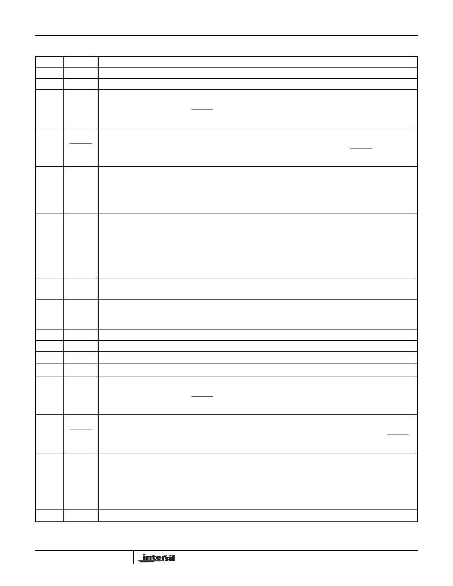
BLOCK DIAGRAM
X4023X Family Selector Guide
X= 256 tap 100 tap 64 Tap
1
1
3
1
5
1
7
1
1
9
1
1
DATA
REGISTER
COMMAND
DECODE &
CONTROL
LOGIC
SDA
SCL
POWER-ON /
LOW VOLTAGE
CR
REGISTER
PROTECT LOGIC
EEPROM
THRESHOLD
RESET LOGIC
4
GENERATION
RESET
V2MON
V
CC
VTRIP
1
V3MON
+
-
2 kbit
RESET
Manual Reset (MR)
8
R
H
R
W
V2FAIL
WP
V3FAIL
ARRAY
2
©2000 Intersil Inc., Patents Pending (VTRIP
1,2,3
are user programmable)
WIPER
REGISTER
R
H
R
W
COUNTER
8 - BIT
NONVOLATILE
MEMORY
256 Tap DCP
Optional
64 or 100 Tap DCP
V
SS
VTRIP
2
VTRIP
3
WIPER
REGISTER
COUNTER
8 - BIT
NONVOLATILE
MEMORY
+
-
≠
+
Data Sheet
April 11, 2005

2
FN8115.0
April 11, 2005
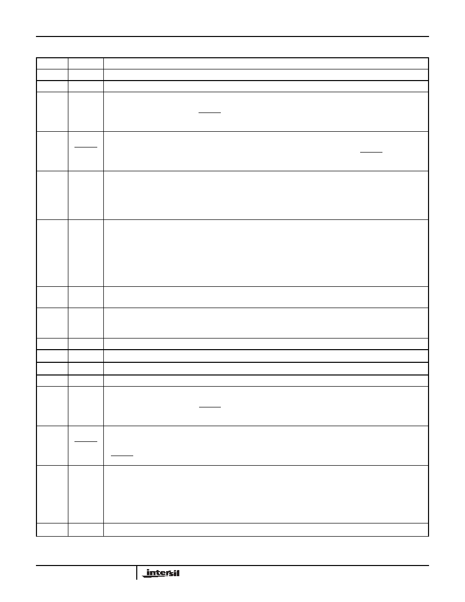
PIN CONFIGURATION
V2MON
V3MON
NC
3
4
V
CC
SDA
R
H0
R
W0
VSS
7
8
V3FAIL
NC
1
14
15
13
16
10
11
9
12
WP
6
NC
2
MR
5
SCL
RESET
V2FAIL
16 Pin SOIC
X40231
V2MON
V3MON
R
W1
3
4
V
CC
SDA
R
H1
NC
VSS
7
8
V3FAIL
NC
1
14
15
13
16
10
11
9
12
WP
6
NC
2
MR
5
SCL
RESET
V2FAIL
16 Pin SOIC
X40233
V2MON
V3MON
NC
3
4
V
CC
SDA
NC
NC
VSS
7
8
V3FAIL
R
H2
1
14
15
13
16
10
11
9
12
WP
6
R
W2
2
MR
5
SCL
RESET
V2FAIL
16 Pin SOIC
X40235
V2MON
V3MON
NC
3
4
V
CC
SDA
R
H0
R
W0
VSS
7
8
V3FAIL
R
H2
1
14
15
13
16
10
11
9
12
WP
6
R
W2
2
MR
5
SCL
RESET
V2FAIL
16 Pin SOIC
X40237
V2MON
V3MON
R
W1
3
4
V
CC
SDA
R
H1
NC
VSS
7
8
V3FAIL
R
H2
1
14
15
13
16
10
11
9
12
WP
6
R
W2
2
MR
5
SCL
RESET
V2FAIL
16 Pin SOIC
X40239
SINGLE XDCP
DUAL XDCP
X40231, X40233, X40235, X40237, X40239
3
FN8115.0
April 11, 2005
X40231 PIN ASSIGNMENT
SOIC
Name
Function
1
NC
No Connect
2
NC
No Connect
3
V3MON
V3MON Voltage Monitor Input.
V3MON i s the input to a non-inverting voltage comparator circuit. When the V3MON input is higher than
the V
TRIP3
threshold voltage, V3FAIL makes a transition to a HIGH level. Connect V3MON to V
SS
when
not used.
4
V3FAIL
V3MON RESET Output.
This open drain output makes a transition to a HIGH level when V3MON is greater than V
TRIP3
and goes
LOW when V3MON is less than VTRIP3. There is no delay circuitry on this pin. The V3FAIL pin requires
the use of an external "pull-up" resistor.
5
MR
Manual Reset.
MR is a TTL level compatible input. Pulling the MR pin active (HIGH) initiates a reset cycle to the RESET
pin (V
CC
RESET Output pin). RESET will remain HIGH for time t
PURST
after MR has returned to it's
normally LOW state. The reset time can be selected using bits PUP1 and PUP0 in the CR Register. The
MR pin requires the use of an external "pull-down" resistor.
6
WP
Write Protect Control Pin.
WP pin is a TTL level compatible input. When held HIGH, Write Protection is enabled. In the enabled
state, this pin prevents all nonvolatile "write" operations. Also, when the Write Protection is enabled, and
the device Block Lock feature is active (i.e. the Block Lock bits are NOT [0,0]), then no "write" (volatile or
nonvolatile) operations can be performed in the device (including the wiper position of any of the
integrated Digitally Controlled Potentiometers (DCPs). The WP pin uses an internal "pull-down" resistor,
thus if left floating the write protection feature is disabled.
7
SCL
Serial Clock.
This is a TTL level compatible input pin used to control the serial bus timing for data input and output.
8
SDA
Serial Data.
SDA is a bidirectional TTL level compatible pin used to transfer data into and out of the device. The SDA
pin input buffer is always active (not gated). This pin requires an external pull up resistor.
9
VSS
Ground.
10
NC
No Connect
11
R
H0
Connection to end of resistor array for (the 64 Tap) DCP.
12
R
W0
Connection to terminal equivalent to the "Wiper" of a mechanical potentiometer for DCP.
13
V2MON
V2MON Voltage Monitor Input.
V2MON is the input to a non-inverting voltage comparator circuit. When the V2MON input is greater than
the V
TRIP2
threshold voltage, V2FAIL makes a transition to a HIGH level. Connect V2MON to V
SS
when
not used.
14
V2FAIL
V2MON RESET Output.
This open drain output makes a transition to a HIGH level when V2MON is greater than V
TRIP2
, and goes
LOW when V2MON is less than V
TRIP2
. There is no power-up reset delay circuitry on this pin. The V2FAIL
pin requires the use of an external "pull-up" resistor.
15
RESET
V
CC
RESET Output.
This is an active HIGH, open drain output which becomes active whenever V
CC
falls below V
TRIP1
. RESET
becomes active on power-up and remains active for a time t
PURST
after the power supply stabilizes
(t
PURST
can be changed by varying the PUP0 and PUP1 bits of the internal control register). The RESET
pin requires the use of an external "pull-up" resistor. The RESET pin can be forced active (HIGH) using
the manual reset (MR) input pin.
16
V
CC
Supply Voltage.
X40231, X40233, X40235, X40237, X40239
4
FN8115.0
April 11, 2005
X40233 PIN ASSIGNMENT
SOIC
Name
Function
1
NC
No Connect
2
NC
No Connect
3
V3MON
V3MON Voltage Monitor Input.
V3MON is the input to a non-inverting voltage comparator circuit. When the V3MON input is higher than
the V
TRIP3
threshold voltage, V3FAIL makes a transition to a HIGH level. Connect V3MON to V
SS
when
not used.
4
V3FAIL
V3MON RESET Output.
This open drain output makes a transition to a HIGH level when V3MON is greater than V
TRIP3
and goes
LOW when V3MON is less than VTRIP3. There is no delay circuitry on this pin. The V3FAIL pin requires
the use of an external "pull-up" resistor.
5
MR
Manual Reset.
MR is a TTL level compatible input. Pulling the MR pin active (HIGH) initiates a reset cycle to the RESET
pin (V
CC
RESET Output pin). RESET will remain HIGH for time t
PURST
after MR has returned to it's
normally LOW state. The reset time can be selected using bits PUP1 and PUP0 in the CR Register. The
MR pin requires the use of an external "pull-down" resistor.
6
WP
Write Protect Control Pin.
WP pin is a TTL level compatible input. When held HIGH, Write Protection is enabled. In the enabled
state, this pin prevents all nonvolatile "write" operations. Also, when the Write Protection is enabled, and
the device Block Lock feature is active (i.e. the Block Lock bits are NOT [0,0]), then no "write" (volatile
or nonvolatile) operations can be performed in the device (including the wiper position of any of the
integrated Digitally Controlled Potentiometers (DCPs). The WP pin uses an internal "pull-down" resistor,
thus if left floating the write protection feature is disabled.
7
SCL
Serial Clock.
This is a TTL level compatible input pin used to control the serial bus timing for data input and output.
8
SDA
Serial Data.
SDA is a bidirectional TTL level compatible pin used to transfer data into and out of the device. The SDA
pin input buffer is always active (not gated). This pin requires an external pull up resistor.
9
VSS
Ground.
10
R
W1
Connection to terminal equivalent to the "Wiper" of a mechanical potentiometer for DCP.
11
R
H1
Connection to end of resistor array for (the 100 Tap) DCP.
12
NC
No Connect
13
V2MON
V2MON Voltage Monitor Input.
V2MON is the input to a non-inverting voltage comparator circuit. When the V2MON input is greater than
the V
TRIP2
threshold voltage, V2FAIL makes a transition to a HIGH level. Connect V2MON to V
SS
when
not used.
14
V2FAIL
V2MON RESET Output.
This open drain output makes a transition to a HIGH level when V2MON is greater than V
TRIP2
, and goes
LOW when V2MON is less than V
TRIP2
. There is no power-up reset delay circuitry on this pin. The
V2FAIL pin requires the use of an external "pull-up" resistor.
15
RESET
V
CC
RESET Output.
This is an active HIGH, open drain output which becomes active whenever V
CC
falls below V
TRIP1
.
RESET becomes active on power-up and remains active for a time t
PURST
after the power supply
stabilizes (t
PURST
can be changed by varying the PUP0 and PUP1 bits of the internal control register).
The RESET pin requires the use of an external "pull-up" resistor. The RESET pin can be forced active
(HIGH) using the manual reset (MR) input pin.
16
V
CC
Supply Voltage.
X40231, X40233, X40235, X40237, X40239
5
FN8115.0
April 11, 2005
X40235 PIN ASSIGNMENT
SOIC
Name
Function
1
R
H2
Connection to end of resistor array for (the 256 Tap) DCP.
2
R
W2
Connection to terminal equivalent to the "Wiper" of a mechanical potentiometer for DCP.
3
V3MON
V3MON Voltage Monitor Input.
V3MON is the input to a non-inverting voltage comparator circuit. When the V3MON input is higher than
the V
TRIP3
threshold voltage, V3FAIL makes a transition to a HIGH level. Connect V3MON to V
SS
when
not used.
4
V3FAIL
V3MON RESET Output.
This open drain output makes a transition to a HIGH level when V3MON is greater than V
TRIP3
and goes
LOW when V3MON is less than VTRIP3. There is no delay circuitry on this pin. The V3FAIL pin requires
the use of an external "pull-up" resistor.
5
MR
Manual Reset.
MR is a TTL level compatible input. Pulling the MR pin active (HIGH) initiates a reset cycle to the RESET
pin (V
CC
RESET Output pin). RESET will remain HIGH for time t
PURST
after MR has returned to it's
normally LOW state. The reset time can be selected using bits PUP1 and PUP0 in the CR Register. The
MR pin requires the use of an external "pull-down" resistor.
6
WP
Write Protect Control Pin.
WP pin is a TTL level compatible input. When held HIGH, Write Protection is enabled. In the enabled
state, this pin prevents all nonvolatile "write" operations. Also, when the Write Protection is enabled, and
the device Block Lock feature is active (i.e. the Block Lock bits are NOT [0,0]), then no "write" (volatile
or nonvolatile) operations can be performed in the device (including the wiper position of any of the
integrated Digitally Controlled Potentiometers (DCPs). The WP pin uses an internal "pull-down" resistor,
thus if left floating the write protection feature is disabled.
7
SCL
Serial Clock.
This is a TTL level compatible input pin used to control the serial bus timing for data input and output.
8
SDA
Serial Data.
SDA is a bidirectional TTL level compatible pin used to transfer data into and out of the device. The SDA
pin input buffer is always active (not gated). This pin requires an external pull up resistor.
9
VSS
Ground.
10
NC
No Connect
11
NC
No Connect
12
NC
No Connect
13
V2MON
V2MON Voltage Monitor Input.
V2MON is the input to a non-inverting voltage comparator circuit. When the V2MON input is greater than
the V
TRIP2
threshold voltage, V2FAIL makes a transition to a HIGH level. Connect V2MON to V
SS
when
not used.
14
V2FAIL
V2MON RESET Output.
This open drain output makes a transition to a HIGH level when V2MON is greater than V
TRIP2
, and goes
LOW when V2MON is less than V
TRIP2
. There is no power-uppower-up reset delay circuitry on this pin.
The V2FAIL pin requires the use of an external "pull-up" resistor.
15
RESET
V
CC
RESET Output.
This is an active HIGH, open drain output which becomes active whenever V
CC
falls below V
TRIP1
.
RESET becomes active on power-up and remains active for a time t
PURST
after the power supply
stabilizes (t
PURST
can be changed by varying the PUP0 and PUP1 bits of the internal control register).
The RESET pin requires the use of an external "pull-up" resistor. The RESET pin can be forced active
(HIGH) using the manual reset (MR) input pin.
16
V
CC
Supply Voltage.
X40231, X40233, X40235, X40237, X40239