1
Æ
FN8126.1
CAUTION: These devices are sensitive to electrostatic discharge; follow proper IC Handling Procedures.
1-888-INTERSIL or 1-888-468-3774
|
Intersil (and design) is a registered trademark of Intersil Americas Inc.
Copyright Intersil Americas Inc. 2005. All Rights Reserved
All other trademarks mentioned are the property of their respective owners.
X5043, X5045
4K, 512 x 8 Bit
CPU Supervisor with 4K SPI EEPROM
These devices combine four popular functions, Power-on
Reset Control, Watchdog Timer, Supply Voltage Supervision,
and Block Lock Protect Serial EEPROM Memory in one
package. This combination lowers system cost, reduces
board space requirements, and increases reliability.
Applying power to the device activates the power-on reset
circuit which holds RESET/RESET active for a period of
time. This allows the power supply and oscillator to stabilize
before the processor executes code.
The Watchdog Timer provides an independent protection
mechanism for microcontrollers. When the microcontroller
fails to restart a timer within a selectable time out interval,
the device activates the RESET/RESET signal. The user
selects the interval from three preset values. Once selected,
the interval does not change, even after cycling the power.
The device's low V
CC
detection circuitry protects the user's
system from low voltage conditions, resetting the system
when V
CC
falls below the minimum V
CC
trip point.
RESET/RESET is asserted until V
CC
returns to proper
operating level and stabilizes. Four industry standard V
TRIP
thresholds are available, however, Intersil's unique circuits
allow the threshold to be reprogrammed to meet custom
requirements or to fine-tune the threshold for applications
requiring higher precision.
The memory portion of the device is a CMOS Serial
EEPROM array with Intersil's block lock protection. The
array is internally organized as 512 x 8. The device features
a Serial Peripheral Interface (SPI) and software protocol
allowing operation on a simple four-wire bus.
The device utilizes Intersil's proprietary Direct Write
TM
cell,
providing a minimum endurance of 100,000 cycles and a
minimum data retention of 100 years.
Features
∑ Low V
CC
Detection and Reset Assertion
- Four standard reset threshold voltages
4.63V, 4.38V, 2.93V, 2.63V
- Re-program low V
CC
reset threshold voltage using
special programming sequence.
- Reset signal valid to V
CC
= 1V
∑ Selectable Time Out Watchdog Timer
∑ Long Battery Life with Low Power Consumption
- <50µA max standby current, watchdog on
- <10µA max standby current, watchdog off
∑ 4Kbits of EEPROM≠1M Write Cycle Endurance
∑ Save Critical Data with Block Lock
TM
Memory
- Protect 1/4, 1/2, all or none of EEPROM array
∑ Built-in Inadvertent Write Protection
- Write enable latch
- Write protect pin
∑ SPI Interface - 3.3MHz Clock Rate
∑ Minimize Programming Time
- 16-byte page write mode
- 5ms write cycle time (typical)
∑ Available Packages
- 8 Ld MSOP, 8 Ld SOIC, 8 Ld PDIP
- 14 Ld TSSOP
∑ Pb-Free Plus Anneal Available (RoHS Compliant)
Applications
∑ Communications Equipment
- Routers, Hubs, Switches
- Set Top Boxes
∑ Industrial Systems
- Process Control
- Intelligent Instrumentation
∑ Computer Systems
- Desktop Computers
- Network Servers
∑ Battery Powered Equipment
Data Sheet
September 16, 2005
5
FN8126.1
September 16, 2005
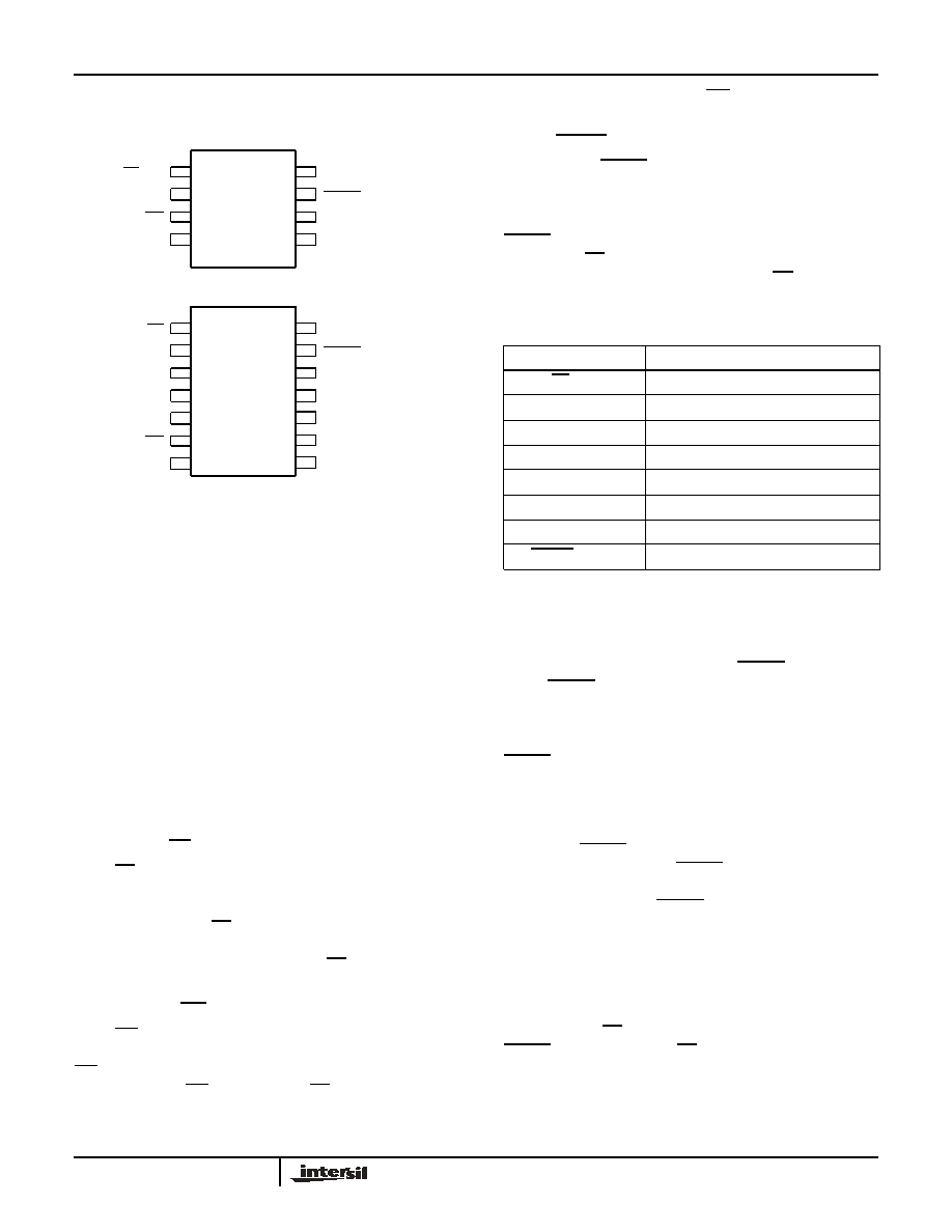
Pin Configuration
Pin Descriptions
Serial Output (SO)
SO is a push/pull serial data output pin. During a read cycle,
data is shifted out on this pin. Data is clocked out by the
falling edge of the serial clock.
Serial Input (SI)
SI is the serial data input pin. All opcodes, byte addresses,
and data to be written to the memory are input on this pin.
Data is latched by the rising edge of the serial clock.
Serial Clock (SCK)
The Serial Clock controls the serial bus timing for data input
and output. Opcodes, addresses, or data present on the SI
pin is latched on the rising edge of the clock input, while data
on the SO pin changes after the falling edge of the clock
input.
Chip Select (CS/WDI)
When CS is high, the X5043, X5045 are deselected and the
SO output pin is at high impedance and, unless an internal
write operation is underway, the X5043, X5045 will be in the
standby power mode. CS low enables the X5043, X5045,
placing it in the active power mode. It should be noted that
after power-up, a high to low transition on CS is required prior
to the start of any operation.
Write Protect (WP)
When WP is low, nonvolatile writes to the X5043, X5045 are
disabled, but the part otherwise functions normally. When
WP is held high, all functions, including non volatile writes
operate normally. WP going low while CS is still low will
interrupt a write to the X5043, X5045. If the internal write
cycle has already been initiated, WP going low will have no
affect on a write.
Reset (RESET, RESET)
X5043, X5045, RESET/RESET is an active low/HIGH, open
drain output which goes active whenever V
CC
falls below the
minimum V
CC
sense level. It will remain active until V
CC
rises above the minimum V
CC
sense level for 200ms.
RESET/RESET also goes active if the Watchdog timer is
enabled and CS remains either high or low longer than the
Watchdog time out period. A falling edge of CS will reset the
watchdog timer.
Principles of Operation
Power-on Reset
Application of power to the X5043, X5045 activate a Power-
on Reset Circuit. This circuit pulls the RESET/RESET pin
active. RESET/RESET prevents the system microprocessor
from starting to operate with insufficient voltage or prior to
stabilization of the oscillator. When V
CC
exceeds the device
V
TRIP
value for 200ms (nominal) the circuit releases
RESET/RESET, allowing the processor to begin executing
code.
Low Voltage Monitoring
During operation, the X5043, X5045 monitor the V
CC
level
and asserts RESET/RESET if supply voltage falls below a
preset minimum V
TRIP
. The RESET/RESET signal prevents
the microprocessor from operating in a power fail or
brownout condition. The RESET/RESET signal remains
active until the voltage drops below 1V. It also remains active
until V
CC
returns and exceeds V
TRIP
for 200ms.
Watchdog Timer
The Watchdog Timer circuit monitors the microprocessor
activity by monitoring the WDI input. The microprocessor
must toggle the CS/WDI pin periodically to prevent an active
RESET/RESET signal. The CS/WDI pin must be toggled
from HIGH to LOW prior to the expiration of the watchdog
time out period. The state of two nonvolatile control bits in
the Status Register determines the watchdog timer period.
The microprocessor can change these watchdog bits. With
8 Ld SOIC/PDIP/MSOP
CS/WDI
WP
SO
1
2
3
4
RESET/RESET
8
7
6
5
V
CC
X5043, X5045
V
SS
SCK
SI
14 Ld TSSOP
CS
NC
SO
1
2
3
4
RESET/RESET
14
13
12
11
V
CC
X5043, X5045
NC
NC
NC
WP
NC
5
6
7
V
SS
NC
10
9
8
SCK
SI
Pin Names
SYMBOL
DESCRIPTION
CS/WDI
Chip Select Input
SO
Serial Output
SI
Serial Input
SCK
Serial Clock Input
WP
Write Protect Input
V
SS
Ground
V
CC
Supply Voltage
RESET/RESET
Reset Output
X5043, X5045