1
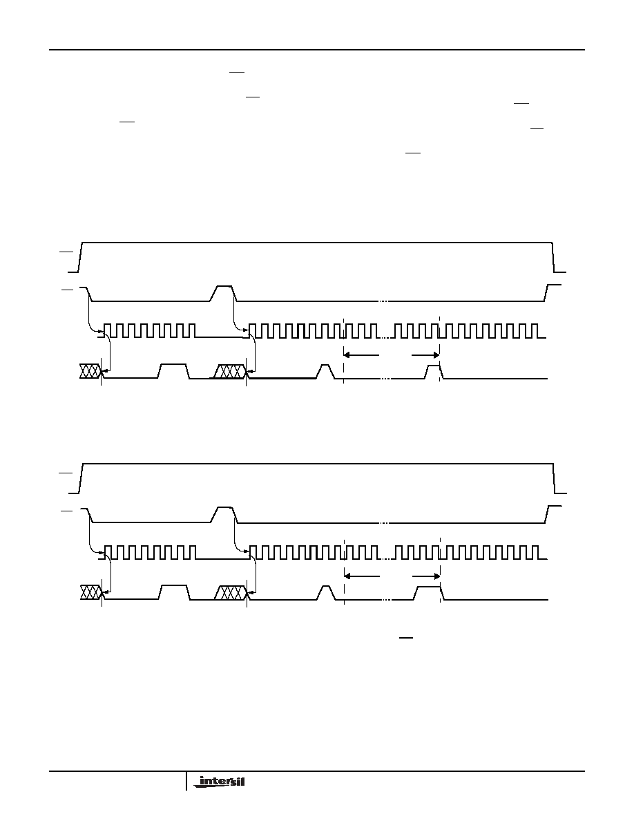
Æ
FN8127.2
CAUTION: These devices are sensitive to electrostatic discharge; follow proper IC Handling Procedures.
1-888-INTERSIL or 1-888-468-3774
|
Intersil (and design) is a registered trademark of Intersil Americas Inc.
Copyright Intersil Americas Inc. 2005. All Rights Reserved
All other trademarks mentioned are the property of their respective owners.
X5083
CPU Supervisor with 8Kbit SPI EEPROM
This device combines four popular functions, Power-on Reset
Control, Watchdog Timer, Supply Voltage Supervision, and
Block Lock Serial EEPROM Memory in one package. This
combination lowers system cost, reduces board space
requirements, and increases reliability.
Applying power to the device activates the power-on reset
circuit which holds RESET active for a period of time. This
allows the power supply and oscillator to stabilize before the
processor can execute code.
The Watchdog Timer provides an independent protection
mechanism for microcontrollers. When the microcontroller fails to
restart a timer within a selectable time out interval, the device
activates the RESET signal. The user selects the interval
from three preset values. Once selected, the interval does
not change, even after cycling the power.
The device's low V
CC
detection circuitry protects the user's
system from low voltage conditions, resetting the system
when V
CC
falls below the minimum V
CC
trip point. RESET is
asserted until V
CC
returns to the proper operating level and
stabilizes. Five industry standard V
TRIP
thresholds are
available, however, Intersil's unique circuits allow the threshold
to be reprogrammed to meet custom requirements or to fine-
tune the threshold for applications requiring higher precision.
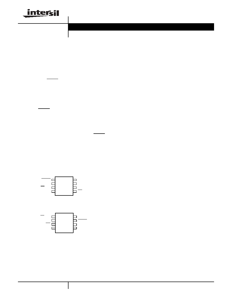
Pinouts
8 Ld TSSOP
8 Ld SOIC, 8 Ld PDIP
Features
∑ Low V
CC
detection and reset assertion
- Four standard reset threshold voltages
4.63V, 4.38V, 2.93V, 2.63V
- Re-program low V
CC
reset threshold voltage using
special programming sequence
- Reset signal valid to V
CC
= 1V
∑ Selectable time out watchdog timer
∑ Long battery life with low power consumption
- <50µA max standby current, watchdog on
- <1µA max standby current, watchdog off
- <400µA max active current during read
∑ 8Kbits of EEPROM
∑ Save critical data with Block Lock
TM
memory
- Block lock first or last page, any 1/4 or lower 1/2 of
EEPROM array
∑ Built-in inadvertent write protection
- Write enable latch
- Write protect pin
∑ SPI Interface - 3.3MHz clock rate
∑ Minimize programming time
- 16 byte page write mode
- 5ms write cycle time (typical)
∑ SPI modes (0,0 & 1,1)
∑ Available packages
- 8 Ld TSSOP, 8 Ld SOIC, 8 Ld PDIP
∑ Pb-free plus anneal available (RoHS compliant)
Applications
∑ Communications Equipment
- Routers, Hubs, Switches
- Set Top Boxes
∑ Industrial Systems
- Process Control
- Intelligent Instrumentation
∑ Computer Systems
- Desktop Computers
- Network Servers
∑ Battery Powered Equipment
SCK
SI
V
SS
WP
V
CC
CS/WDI
SO
1
2
3
4
8
7
6
5
X5083
RESET
X5083
CS/WDI
WP
SO
1
2
3
4
RESET
8
7
6
5
V
CC
V
SS
SCK
SI
Data Sheet
September 16, 2005
2
FN8127.2
September 16, 2005
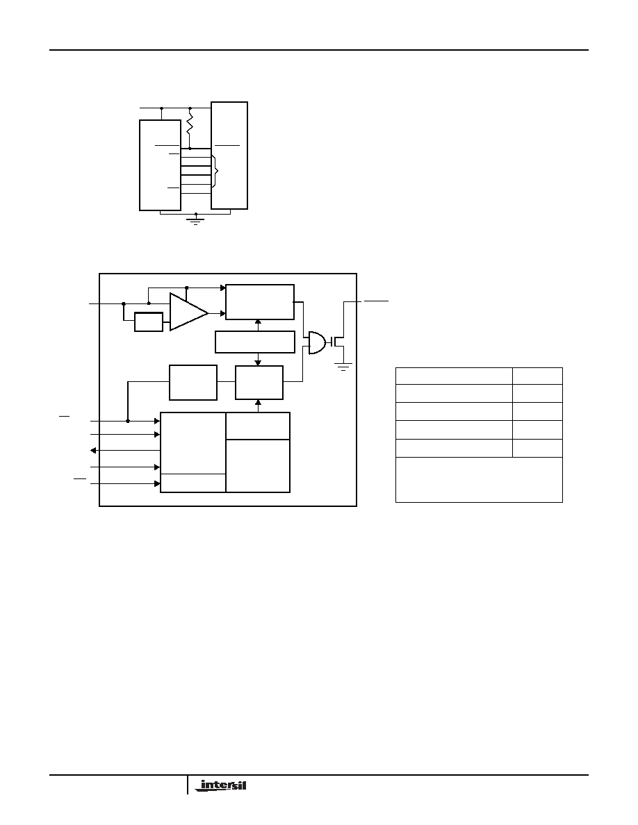
Typical Application
Block Diagram
uC
RESET
CS
SCK
SI
SO
WP
VCC
VSS
RESET
SPI
VCC
VSS
X5083
2.7-5.0V
10K
WATCHDOG
TIMER
COMMAND
DECODE &
CONTROL
LOGIC
SI
SO
SCK
CS/WDI
V
CC
POR AND LOW
GENERATION
V
TRIP
+
-
RESET (X5083)
VOLTAGE RESET
PROTECT LOGIC
8KBITS
EEPROM
WATCHDOG
DETECTOR
WP
ARRAY
STATUS
REGISTER
TRANSITION
RESET
RESET & WATCHDOG
TIMEBASE
X5083
STANDARD V
TRIP
LEVEL
SUFFIX
4.63V (+/-2.5%)
-4.5A
4.38V (+/-2.5%)
-4.5
2.93V (+/-2.5%)
-2.7A
2.63V (+/-2.5%)
-2.7
See "Ordering Information" on page 3 for
more details
For Custom Settings, call Intersil.
X5083
3
FN8127.2
September 16, 2005
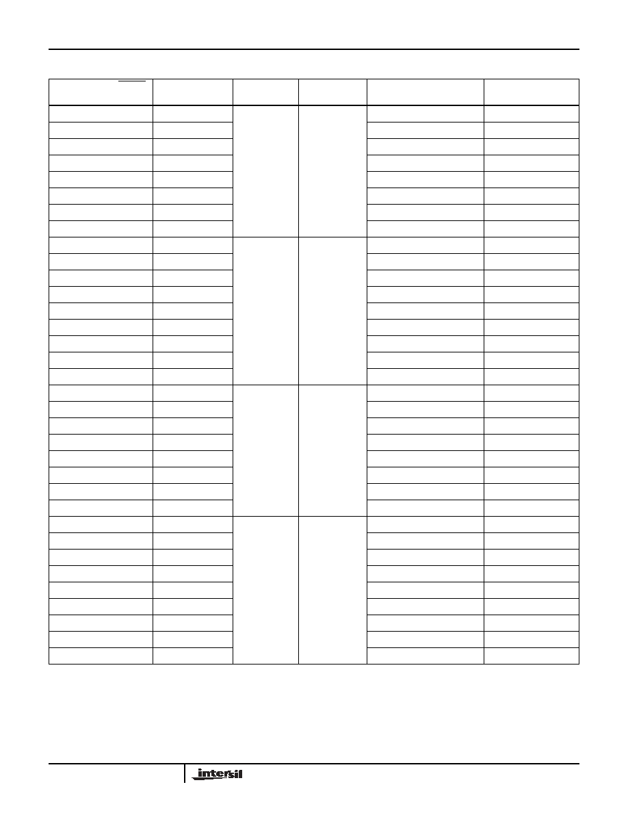
Ordering Information
PART NUMBER RESET
(ACTIVE LOW)
PART MARKING
V
CC
RANGE (V)
V
TRIP
RANGE
TEMPERATURE RANGE (∞C)
PACKAGE
X5083P-4.5A
X5083P AL
4.5-5.5
4.5-4.75
0 to 70
8 Ld PDIP
X5083PI-4.5A
X5083P AM
-40 to 85
8 Ld PDIP
X5083S8-4.5A
X5083 AL
0 to 70
8 Ld SOIC
X5083S8Z-4.5A (Note)
X5083 Z AL
0 to 70
8 Ld SOIC (Pb-free)
X5083S8I-4.5A*
X5083 AM
-40 to 85
8 Ld SOIC
X5083S8IZ-4.5A* (Note)
X5083 Z AM
-40 to 85
8 Ld SOIC (Pb-free)
X5083V8-4.5A
583AL
0 to 70
8 Ld TSSOP
X5083V8I-4.5A
583AM
-40 to 85
8 Ld TSSOP
X5083P
X5083P
4.5-5.5
4.25-4.5
0 to 70
8 Ld PDIP
X5083PI
X5083P I
-40 to 85
8 Ld PDIP
X5083SI
X5083 I
-40 to 85
8 Ld SOIC
X5083S8
X5083
0 to 70
8 Ld SOIC
X5083S8Z (Note)
X5083 Z
0 to 70
8 Ld SOIC (Pb-free)
X5083S8I*
X5083 I
-40 to 85
8 Ld SOIC
X5083S8IZ* (Note)
X5083 Z I
-40 to 85
8 Ld SOIC (Pb-free)
X5083V8
X583
0 to 70
8 Ld TSSOP
X5083V8I
583I
-40 to 85
8 Ld TSSOP
X5083P-2.7A
X5083P AN
2.7-5.5
2.85-3.0
0 to 70
8 Ld PDIP
X5083PI-2.7A
X5083P AP
-40 to 85
8 Ld PDIP
X5083S8-2.7A
X5083 AN
0 to 70
8 Ld SOIC
X5083S8Z-2.7A (Note)
X5083 Z AN
0 to 70
8 Ld SOIC (Pb-free)
X5083S8I-2.7A
X5083 AP
-40 to 85
8 Ld SOIC
X5083S8IZ-2.7A (Note)
X5083 Z AP
-40 to 85
8 Ld SOIC (Pb-free)
X5083V8-2.7A
583AN
0 to 70
8 Ld TSSOP
X5083V8I-2.7A
583AP
-40 to 85
8 Ld TSSOP
X5083P-2.7
X5083P F
2.7-5.5
2.55-2.7
0 to 70
8 Ld PDIP
X5083PI-2.7
X5083P G
-40 to 85
8 Ld PDIP
X5083S8-2.7*
X5083 F
0 to 70
8 Ld SOIC
X5083S8Z-2.7* (Note)
X5083 Z F
0 to 70
8 Ld SOIC (Pb-free)
X5083S8I-2.7*
X5083 G
-40 to 85
8 Ld SOIC
X5083S8IZ-2.7* (Note)
X5083 Z G
-40 to 85
8 Ld SOIC (Pb-free)
X5083V8-2.7
583F
0 to 70
8 Ld TSSOP
X5083V8I-2.7
583G
-40 to 85
8 Ld TSSOP
X5083V8IZ-2.7 (Note)
-40 to 85
8 Ld TSSOP (Pb-free)
NOTE: Intersil Pb-free plus anneal products employ special Pb-free material sets; molding compounds/die attach materials and 100% matte tin plate
termination finish, which are RoHS compliant and compatible with both SnPb and Pb-free soldering operations. Intersil Pb-free products are MSL
classified at Pb-free peak reflow temperatures that meet or exceed the Pb-free requirements of IPC/JEDEC J STD-020.
*Add "-T1" suffix for tape and reel.
X5083
4
FN8127.2
September 16, 2005
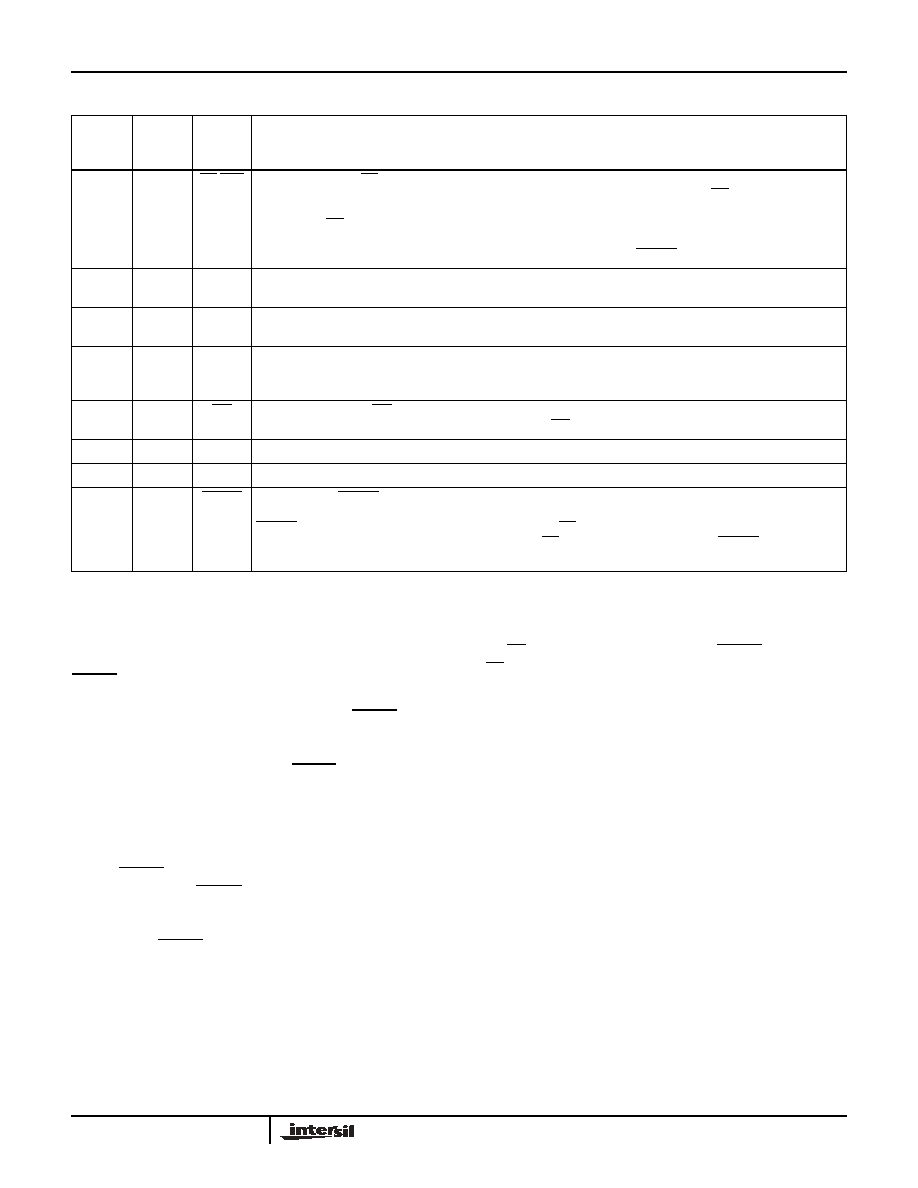
Pin Description
Principles of Operation
Power-on Reset
Application of power to the X5083 activates a power-on
reset circuit. This circuit goes LOW at 1V and pulls the
RESET pin active. This signal prevents the system
microprocessor from starting to operate with insufficient
voltage or prior to stabilization of the oscillator. RESET
active also blocks communication to the device through the
SPI interface. When V
CC
exceeds the device V
TRIP
value for
200ms (nominal) the circuit releases RESET, allowing the
processor to begin executing code. While V
CC
< V
TRIP
communications to the device are inhibited.
Low Voltage Monitoring
During operation, the X5083 monitors the V
CC
level and
asserts RESET if supply voltage falls below a preset
minimum V
TRIP
. The RESET signal prevents the
microprocessor from operating in a power fail or brownout
condition and terminates any SPI communication in
progress. The RESET signal remains active until the voltage
drops below 1V. It also remains active until V
CC
returns and
exceeds V
TRIP
for 200ms.
When V
CC
falls below V
TRIP
, any communications in
progress are terminated and communications are inhibited
until V
CC
exceeds V
TRIP
for t
PURST
.
Watchdog Timer
The watchdog timer circuit monitors the microprocessor activity
by monitoring the WDI input. The microprocessor must toggle
the CS/WDI pin periodically to prevent a RESET signal. The
CS/WDI pin must be toggled from HIGH to LOW prior to the
expiration of the watchdog time out period. The state of two
nonvolatile control bits in the status register determine the
watchdog timer period. The microprocessor can change these
watchdog bits with no action taken by the microprocessor
these bits remain unchanged, even after total power failure.
V
CC
Threshold Reset Procedure
The X5083 is shipped with a standard V
CC
threshold (V
TRIP
)
voltage. This value will not change over normal operating
and storage conditions. However, in applications where the
standard V
TRIP
is not exactly right, or if higher precision is
needed in the V
TRIP
value, the X5083 threshold may be
adjusted. The procedure is described below, and uses the
application of a high voltage control signal.
Setting the V
TRIP
Voltage
This procedure is used to set the V
TRIP
to a higher voltage
value. For example, if the current V
TRIP
is 4.4V and the new
V
TRIP
is 4.6V, this procedure will directly make the change. If
the new setting is to be lower than the current setting, then it
is necessary to reset the trip point before setting the new
value.
PIN
(SOIC/
PDIP)
PIN
TSSOP
NAME
FUNCTION
1
3
CS/WDI Chip Select Input. CS HIGH, deselects the device and the SO output pin is at a high impedance state. Unless
a nonvolatile write cycle is underway, the device will be in the standby power mode. CS LOW enables the
device, placing it in the active power mode. Prior to the start of any operation after power-up, a HIGH to LOW
transition on CS is required.
Watchdog Input. A HIGH to LOW transition on the WDI pin restarts the Watchdog timer. The absence of a
HIGH to LOW transition within the watchdog time out period results in RESET going active.
2
4
SO
Serial Output. SO is a push/pull serial data output pin. A read cycle shifts data out on this pin. The falling edge of the
serial clock (SCK) clocks the data out.
5
7
SI
Serial Input. SI is a serial data input pin. Input all opcodes, byte addresses, and memory data on this pin. The rising
edge of the serial clock (SCK) latches the input data. Send all opcodes (Table 1), addresses and data MSB first.
6
8
SCK
Serial Clock. The Serial Clock controls the serial bus timing for data input and output. The rising edge of SCK latches
in the opcode, address, or data bits present on the SI pin. The falling edge of SCK changes the data output on the SO
pin.
3
5
WP
Write Protect. When WP is LOW, nonvolatile write operations to the memory are prohibited. This "Locks" the
memory to protect it against inadvertent changes when WP is HIGH, the device operates normally.
4
6
V
SS
Ground
8
2
V
CC
Supply Voltage
7
1
RESET
Reset Output. RESET is an active LOW, open drain output which goes active whenever V
CC
falls below the
minimum V
CC
sense level. It will remain active until V
CC
rises above the minimum V
CC
sense level for 250ms.
RESET goes active if the watchdog timer is enabled and CS remains either HIGH or LOW longer than the
selectable watchdog time out period. A falling edge of CS will reset the watchdog timer. RESET goes active on
power-up at about 1V and remains active for 250ms after the power supply stabilizes.
X5083
5
FN8127.2
September 16, 2005
To set the new V
TRIP
voltage, apply the desired V
TRIP
threshold voltage to the V
CC
pin and tie the WP pin to the
programming voltage V
P
. Then send a WREN command,
followed by a write of Data 00h to address 01h. CS going
HIGH on the write operation initiates the V
TRIP
programming
sequence. Bring WP LOW to complete the operation.
Note: This operation also writes 00h to array address 01h.
Resetting the V
TRIP
Voltage
This procedure is used to set the V
TRIP
to a "native" voltage
level. For example, if the current V
TRIP
is 4.4V and the new
V
TRIP
must be 4.0V, then the V
TRIP
must be reset. When
V
TRIP
is reset, the new V
TRIP
is something less than 1.7V.
This procedure must be used to set the voltage to a lower
value.
To reset the new V
TRIP
voltage, apply the desired V
TRIP
threshold voltage to the Vcc pin and tie the WP pin to the
programming voltage V
P
. Then send a WREN command,
followed by a write of data 00h to address 03h. CS going
HIGH on the write operation initiates the V
TRIP
programming
sequence. Bring WP
LOW to complete the operation.
Note: This operation also writes 00h to array address 03h.
0 1 2 3 4 5 6 7
SCK
SI
CS
06h
0 1 2 3 4 5 6 7 8 9 10
20 21 22 23
16 Bits
0001h
02h
WP
V
P
= 15-18V
00h
WREN
Write
Address
Data
FIGURE 1. SET V
TRIP
LEVEL SEQUENCE (V
CC
= DESIRED V
TRIP
VALUE)
0 1 2 3 4 5 6 7
SCK
SI
CS
06h
0 1 2 3 4 5 6 7 8 9 10
20 21 22 23
16 Bits
0003h
02h
WP
V
P
= 15-18V
00h
WREN
Write
Address
Data
FIGURE 2. RESET V
TRIP
LEVEL SEQUENCE (V
CC
> 3V. WP = 15-18V)
X5083

6
FN8127.2
September 16, 2005
1
2
3
4
8
7
6
5
X5083
V
TRIP
Adj.
V
P
RESET
4.7K
SI
SO
CS
SCK
µC
Adjust
Run
FIGURE 3. SAMPLE V
TRIP
RESET CIRCUIT
V
TRIP
Programming
Apply 5V to V
CC
Decrement V
CC
RESET pin
goes active?
Measured V
TRIP
-
Desired V
TRIP
DONE
Execute
Sequence
Reset V
TRIP
Set V
CC
= V
CC
Applied =
Desired V
TRIP
Execute
Sequence
Set V
TRIP
New V
CC
Applied =
Old V
CC
Applied + Error
(V
CC
= V
CC
- 50mV)
Execute
Sequence
Reset V
TRIP
New V
CC
Applied =
Old V
CC
Applied - Error
Error
≠Emax
≠Emax < Error < Emax
YES
NO
Error
Emax
Emax = Maximum Desired Error
FIGURE 4. V
TRIP
PROGRAMMING SEQUENCE
X5083

7
FN8127.2
September 16, 2005
SPI Serial Memory
The memory portion of the device is a CMOS serial EEPROM
array with Intersil's block lock protection. The array is
internally organized as x 8. The device features a Serial
Peripheral Interface (SPI) and software protocol allowing
operation on a simple four-wire bus.
The device utilizes Intersil's proprietary Direct Write
TM
cell,
providing a minimum endurance of 100,000 cycles and a
minimum data retention of 100 years.
The device is designed to interface directly with the
synchronous Serial Peripheral Interface (SPI) of many
popular microcontroller families.
The device monitors the bus and asserts RESET output if the
watchdog timer is enabled and there is no bus activity within
the user selectable time out period or the supply voltage falls
below a preset minimum V
TRIP
.
The device contains an 8-bit instruction register. It is
accessed via the SI input, with data being clocked in on the
rising edge of SCK. CS must be LOW during the entire
operation.
All instructions (Table 1), addresses and data are transferred
MSB first. Data input on the SI line is latched on the first
rising edge of SCK after CS goes LOW. Data is output on the
SO line by the falling edge of SCK. SCK is static, allowing
the user to stop the clock and then start it again to resume
operations where left off.
Write Enable Latch
The device contains a Write Enable Latch. This latch must
be SET before a Write Operation is initiated. The WREN
instruction will set the latch and the WRDI instruction will
reset the latch (Figure 7). This latch is automatically reset
upon a power-up condition and after the completion of a
valid Write Cycle.
Status Register
The RDSR instruction provides access to the status register.
The status register may be read at any time, even during a
write cycle. The status register is formatted as follows.
Block Lock Memory
Intersil's block lock memory provides a flexible mechanism to
store and lock system ID and parametric information. There
are seven distinct block lock memory areas within the array
which vary in size from one page to as much as half of the
entire array. These areas and associated address ranges are
block locked by writing the appropriate two byte block lock
instruction to the device as described in Table 1 and Figure 9.
Once a block lock instruction has been completed, that block
lock setup is held in the nonvolatile status register until the
next block lock instruction is issued. The sections of the
memory array that are block locked can be read but not
written until block lock is removed or changed.
Status Register/Block Lock/WDT Byte
7
6
5
4
3
2
1
0
0
0
0
WD1
WD0
BL2
BL1
BL0
TABLE 1. INSTRUCTION SET AND BLOCK LOCK PROTECTION BYTE DEFINITION
INSTRUCTION FORMAT
INSTRUCTION NAME AND OPERATION
0000 0110
WREN: set the write enable latch (write enable operation)
0000 0100
WRDI: reset the write enable latch (write disable operation)
0000 0001
Write status instruction--followed by:
Block lock/WDT byte: (See Figure 1)
000WD
1
WD
2
000 --->no block lock: 00h-00h--->none of the array
000WD
1
WD
2
001 --->block lock Q1: 0000h-00FFh--->lower quadrant (Q1)
000WD
1
WD
2
010 --->block lock Q2: 0100h-01FFh--->Q2
000WD
1
WD
2
011 --->block lock Q3: 0200h-02FFh--->Q3
000WD
1
WD
2
100 --->block lock Q4: 0300h-03FFh--->upper quadrant (Q4)
000WD
1
WD
2
101 --->block lock H1: 0000h-01FFh--->lower half of the array (H1)
000WD
1
WD
2
110 --->block lock P0: 0000h-000Fh--->lower page (P0)
000WD
1
WD
2
111 --->block lock Pn: 03F0h-03FFh--->upper page (PN)
0000 0101
READ STATUS: reads status register & provides write in progress status on SO pin
0000 0010
WRITE: write operation followed by address and data
0000 0011
READ: read operation followed by address
X5083

8
FN8127.2
September 16, 2005
Watchdog Timer
The watchdog timer bits, WD0 and WD1, select the
watchdog time out period. These nonvolatile bits are
programmed with the WRSR instruction. A change to the
Watchdog Timer, either setting a new time out period or
turning it off or on, takes effect, following either the next
command (read or write) or cycling the power to the device.
The recommended procedure for changing the Watch-dog
Timer settings is to do a WREN, followed by a write status
register command. Then execute a soft-ware loop to read
the status register until the MSB of the status byte is zero. A
valid alternative is to do a WREN, followed by a write status
register command. Then wait 10ms and do a read status
command.
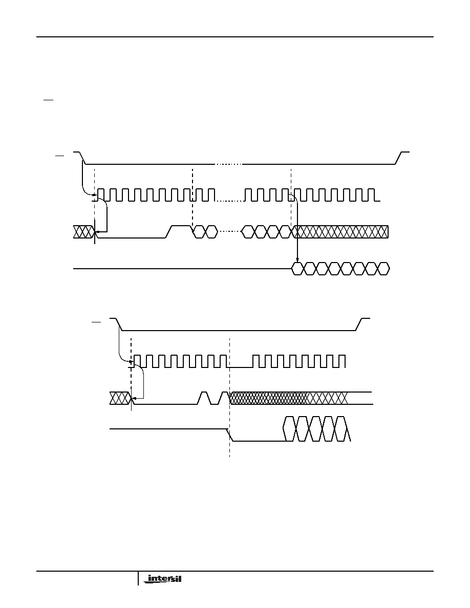
Read Sequence
When reading from the EEPROM memory array, CS is first
pulled low to select the device. The 8-bit READ instruction is
transmitted to the device, followed by the 16-bit address.
After the READ opcode and address are sent, the data
stored in the memory at the selected address is shifted out
on the SO line. The data stored in memory at the next
address can be read sequentially by continuing to provide
clock pulses. The address is automatically incremented to
the next higher address after each byte of data is shifted out.
When the highest address is reached, the address counter
rolls over to address $0000 allowing the read cycle to be
continued indefinitely. The read operation is terminated by
taking CS high. Refer to the read EEPROM array sequence
(Figure 5).
To read the status register, the CS line is first pulled low to
select the device followed by the 8-bit RDSR instruction.
After the RDSR opcode is sent, the contents of the status
register are shifted out on the SO line. Refer to the read status
register sequence (Figure 6).
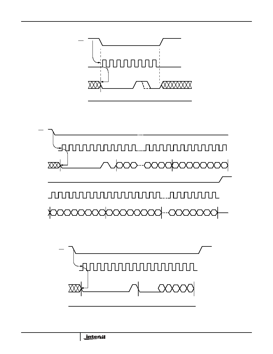
Write Sequence
Prior to any attempt to write data into the device, the "Write
Enable" Latch (WEL) must first be set by issuing the WREN
instruction (Figure 7). CS is first taken LOW, then the WREN
instruction is clocked into the device. After all eight bits of the
instruction are transmitted, CS must then be taken HIGH. If
the user continues the write operation without taking CS
HIGH after issuing the WREN instruction, the write operation
will be ignored.
To write data to the EEPROM memory array, the user then
issues the WRITE instruction followed by the 16 bit address
and then the data to be written. Any unused address bits are
specified to be "0's". The WRITE operation minimally takes
32 clocks. CS must go low and remain low for the duration of
the operation. If the address counter reaches the end of a
page and the clock continues, the counter will roll back to the
first address of the same page and overwrite any data that
may have been previously written.
For a write operation (byte or page write) to be completed,
CS can only be brought HIGH after bit 0 of the last data byte
to be written is clocked in. If it is brought HIGH at any other
time, the write operation will not be completed (Figure 8).
To write to the status register, the WRSR instruction is
followed by the data to be written (Figure 9). Data bits 5, 6
and 7 must be "0".
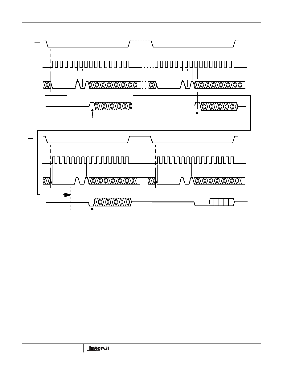
Read Status Operation
If there is not a nonvolatile write in progress, the read status
instruction returns the block lock setting from the status
register which contains the watchdog timer bits WD1, WD0,
and the block lock bits IDL2-IDL0 (Figure 6). The block lock
bits define the block lock condition (Table 1). The watchdog
timer bits set the operation of the watchdog timer (Table 2).
The other bits are reserved and will return '0' when read. See
Figure 6.
During an internal nonvolatile write operaiton, the Read
Status Instruction returns a HIGH on SO in the first bit
following the RDSR instruction (the MSB). The remaining
bits in the output status byte are undefined. Repeated Read
Status Instructions return the MSB as a `1' until the
nonvolatile write cycle is complete. When the nonvolatile
write cycle is completed, the RDSR instruction returns a `0'
in the MSB position with the remaining bits of the status
register undefined. Subsequent RDSR instructions return
the Status Register Contents. See Figure 10.
RESET Operation
The RESET output is designed to go LOW whenever V
CC
has dropped below the minimum trip point and/or the
watchdog timer has reached its programmable time out limit.
The RESET output is an open drain output and requires a
pull up resistor.
Operational Notes
The device powers-up in the following state:
∑ The device is in the low power standby state.
∑ A HIGH to LOW transition on CS is required to enter an
active state and receive an instruction.
∑ SO pin is high impedance.
∑ The write enable latch is reset.
∑ Reset signal is active for t
PURST
.
TABLE 2. WATCHDOG TIMER DEFINITION
STATUS REGISTER BITS
WATCHDOG TIME OUT
(TYPICAL)
WD1
WD0
0
0
1.4s
0
1
600ms
1
0
200ms
1
1
disabled (factory default)
X5083
9
FN8127.2
September 16, 2005
Data Protection
The following circuitry has been included to prevent
inadvertent writes:
∑ A WREN instruction must be issued to set the write enable
latch.
∑ CS must come HIGH at the proper clock count in order to
start a nonvolatile write cycle.
∑ When V
CC
is below V
TRIP
, communications to the device
are inhibited.
0
1
2
3
4
5
6
7
8
9
CS
SCK
SI
SO
High Impedance
Read Instruction
(1 Byte)
Byte Address (2 Byte)
Data Out
15 14
3
2
1
0
20 21 22 23 24 25 26 27 28 29 30
7
6
5
4
3
2
1
0
FIGURE 5. READ OPERATION SEQUENCE
0
1
2
3
4
5
6
7
CS
SCK
SI
SO
Read Status
Instruction
SO = Status Reg When no Nonvolatile
Write Cycle
...
...
...
B
L
2
B
L
1
B
L
0
W
D
0
W
D
1
FIGURE 6. READ STATUS OPERATION SEQUENCE
X5083
10
FN8127.2
September 16, 2005
0
1
2
3
4
5
6
7
CS
SI
SCK
High Impedance
SO
Instruction
(1 Byte)
FIGURE 7. WREN/WRDI SEQUENCE
32 33 34 35 36 37 38 39
SCK
SI
CS
0
1
2
3
4
5
6
7
8
9
10
SCK
SI
Instruction
16 Bit Address
Data Byte 1
7
6
5
4
3
2
1
0
CS
40 41 42 43 44 45 46 47
Data Byte 2
7
6
5
4
3
2
1
0
Data Byte 3
7
6
5
4
3
2
1
0
Data Byte N
15 14 13
3
2
1
0
20 21 22 23 24 25 26 27 28 29 30 31
6
5
4
3
2
1
0
FIGURE 8. EEPROM ARRAY WRITE SEQUENCE
0
1
2
3
4
5
6
7
8
9
CS
SCK
SI
SO
High Impedance
Instruction
10 11 12 13 14 15
Data Byte
6
5
4
3
2
1
0
W
D
1
W
D
0
B
L
2
L
1
L
0
B
B
FIGURE 9. STATUS REGISTER WRITE SEQUENCE
X5083
11
FN8127.2
September 16, 2005
0 1 2 3 4 5 6 7
CS
SCK
SI
SO
SO MSB HIGH while
in the Nonvolatile write cycle
0 1 2 3 4 5 6 7
READ STATUS
INSTRUCTION
READ STATUS
INSTRUCTION
SO MSB still HIGH indicates
Nonvolatile write cycle still in progress
0 1 2 3 4 5 6 7
CS
SCK
SI
SO
0 1 2 3 4 5 6 7
READ STATUS
INSTRUCTION
READ STATUS
INSTRUCTION
1st detected SO MSB LOW
indicates end of Nonvolatile write cycle
4 3 2 1 0
WD1
WD0
BL2
BL1
BL0
NONVOLATILE WRITE IN PROGRESS
NONVOLATILE
WRITE ENDS
FIGURE 10. READ NONVOLATILE WRITE STATUS
X5083
12
FN8127.2
September 16, 2005
Symbol Table
0
1
2
3
4
5
CS
SCK
SI
INSTRUCTION
t
WC
Non-volatile
Write
Operation
6
7
NEXT
Wait t
WC
after a write for new operation,
if not using polling procedure
FIGURE 11. END OF NONVOLATILE WRITE (NO POLLING)
WAVEFORM
INPUTS
OUTPUTS
Must be
steady
Will be
steady
May change
from LOW
to HIGH
Will change
from LOW
to HIGH
May change
from HIGH
to LOW
Will change
from HIGH
to LOW
Don't Care:
Changes
Allowed
Changing:
State Not
Known
N/A
Center Line
is High
Impedance
X5083

13
FN8127.2
September 16, 2005
.
Absolute Maximum Ratings
Operating Conditions
Temperature Under Bias . . . . . . . . . . . . . . . . . . . . . .-65∞C to 135∞C
Storage Temperature . . . . . . . . . . . . . . . . . . . . . . . .-65∞C to 150∞C
Voltage on Any Pin with Respect To V
ss
. . . . . . . . . . . . . -1.0V to 7V
D.C. Output Current . . . . . . . . . . . . . . . . . . . . . . . . . . . . . . . . . . 5mA
Lead Temperature (Soldering, 10s) . . . . . . . . . . . . . . . . . . . . . 300∞C
Temperature Range
Commercial . . . . . . . . . . . . . . . . . . . . . . . . . . . . . . . . . 0∞C to 70∞C
Industrial . . . . . . . . . . . . . . . . . . . . . . . . . . . . . . . . . . -40∞C to 85∞C
V
CC
Range
-2.7. . . . . . . . . . . . . . . . . . . . . . . . . . . . . . . . . . . . . . . . 2.7V to 5.5V
Blank . . . . . . . . . . . . . . . . . . . . . . . . . . . . . . . . . . . . . . 4.5V to 5.5V
CAUTION: Stresses above those listed in "Absolute Maximum Ratings" may cause permanent damage to the device. This is a stress only rating and operation of the
device at these or any other conditions above those indicated in the operational sections of this specification is not implied.
DC Electrical Specifications
(Over the recommended operating conditions unless otherwise specified.)
SYMBOL
PARAMETER
TEST CONDITIONS
LIMITS
UNIT
MIN
TYP
MAX
I
CC1
V
CC
Write Current (Active)
SCK = V
CC
x 0.1/V
CC
x 0.9 @ 5MHz,
SO = Open
5
mA
I
CC2
V
CC
Read Current (Active)
SCK = V
CC
x 0.1/V
CC
x 0.9 @ 5MHz,
SO = Open
0.4
mA
I
SB1
V
CC
Standby Current WDT = OFF CS = V
CC
, V
IN
= V
SS
or V
CC
,
V
CC
= 5.5V
1
µA
I
SB2
V
CC
Standby Current WDT = ON
CS = V
CC
, V
IN
= V
SS
or V
CC
,
V
CC
= 5.5V
50
µA
I
SB3
V
CC
Standby Current WDT = ON
CS = V
CC
, V
IN
= V
SS
or V
CC
,
V
CC
= 3.6V
20
µA
I
LI
Input Leakage Current
V
IN
= V
SS
to V
CC
0.1
10
µA
I
LO
Output Leakage Current
V
OUT
= V
SS
to V
CC
0.1
10
µA
V
IL
(Note 1) Input LOW Voltage
-0.5
V
CC
x 0.3
V
V
IH
(Note 1) Input HIGH Voltage
V
CC
x 0.7
V
CC
+ 0.5
V
V
OL1
Output LOW Voltage
V
CC
> 3.3V, I
OL
= 2.1mA
0.4
V
V
OL2
Output LOW Voltage
2V < V
CC
3.3V, I
OL
= 1mA
0.4
V
V
OL3
Output LOW Voltage
V
CC
2V, I
OL
= 0.5mA
0.4
V
V
OH1
Output HIGH Voltage
V
CC
> 3.3V, I
OH
= -1.0mA
V
CC
- 0.8
V
V
OH2
Output HIGH Voltage
2V < V
CC
3.3V, I
OH
= -0.4mA
V
CC
- 0.4
V
V
OH3
Output HIGH Voltage
V
CC
2V, I
OH
= -0.25mA
V
CC
- 0.2
V
V
OLRS
Reset Output LOW Voltage
I
OL
= 1mA
0.4
V
Power-Up Timing
SYMBOL
PARAMETER
MIN
MAX
UNIT
t
PUR
(Note 2)
Power-up to read operation
1
ms
t
PUW
(Note 2)
Power-up to write operation
5
ms
Capacitance
T
A
= +25∞C, f = 1MHz, V
CC
= 5V
SYMBOL
TEST
MAX
UNIT
CONDITIONS
C
OUT
(Note 2) Output capacitance (SO, RESET, RESET)
8
pF
V
OUT
= 0V
C
IN
(Note 2)
Input capacitance (SCK, SI, CS, WP)
6
pF
V
IN
= 0V
NOTES:
1. V
IL
min. and V
IH
max. are for reference only and are not tested.
2. This parameter is periodically sampled and not 100% tested.
X5083
14
FN8127.2
September 16, 2005
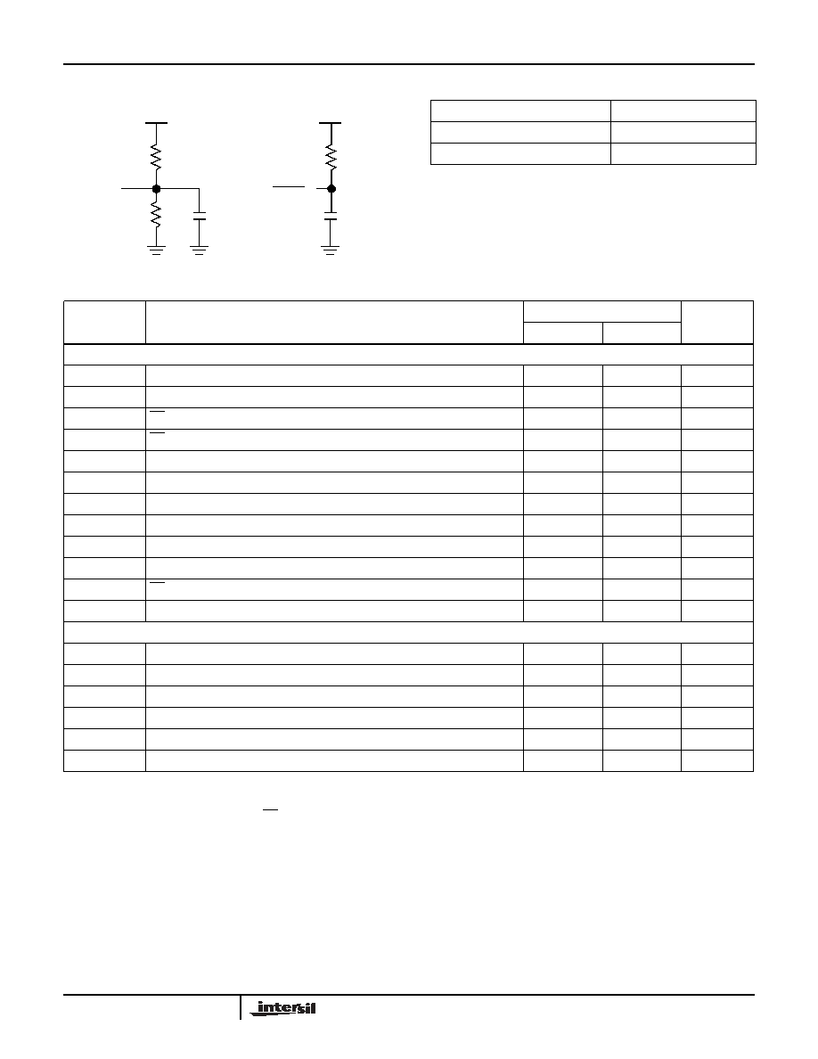
Equivalent A.C. Load Circuit at 5V V
CC
5V
SO
100pF
5V
3.3k
RESET
30pF
1.64k
1.64k
OUTPUT
A.C. Test Conditions
Input pulse levels
V
CC
x 0.1 to V
CC
x 0.9
Input rise and fall times
10ns
Input and output timing level
V
CC
x 0.5
AC Electrical Specifications
(Over recommended operating conditions, unless otherwise specified)
SYMBOL PARAMETER
2.7V-5.5V
UNIT
MIN
MAX
DATA INPUT TIMING
f
SCK
Clock frequency
0
3.3
MHz
t
CYC
Cycle time
300
ns
t
LEAD
CS lead time
150
ns
t
LAG
CS lag time
150
ns
t
WH
Clock HIGH time
130
ns
t
WL
Clock LOW time
130
ns
t
SU
Data setup time
20
ns
t
H
Data hold time
20
ns
t
RI
(Note 3)
Input rise time
2
µs
t
FI
(Note 3)
Input fall time
2
µs
t
CS
CS deselect time
100
ns
t
WC
(Note 4)
Write cycle time
10
ms
DATA OUTPUT TIMING
f
SCK
Clock frequency
0
3.3
MHz
t
DIS
Output disable time
150
ns
t
V
Output valid from clock low
130
ns
t
HO
Output hold time
0
ns
t
RO
(Note 3)
Output rise time
50
ns
t
FO
(Note 3)
Output fall time
50
ns
NOTES:
3. This parameter is periodically sampled and not 100% tested.
4. t
WC
is the time from the rising edge of CS after a valid write sequence has been sent to the end of the self-timed internal nonvolatile write cycle.
X5083
15
FN8127.2
September 16, 2005
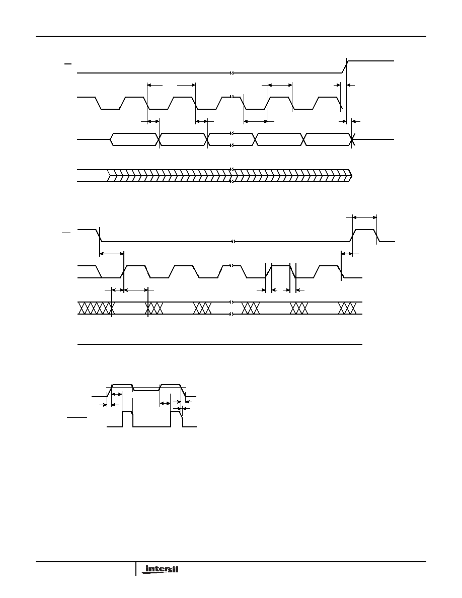
Serial Output Timing
Serial Input Timing
Power-Up and Power-Down Timing
SCK
CS
SO
SI
MSB Out
MSB≠1 Out
LSB Out
ADDR
LSB IN
t
CYC
t
V
t
HO
t
WL
t
WH
t
DIS
t
LAG
SCK
CS
SI
SO
MSB IN
t
SU
t
RI
t
LAG
t
LEAD
t
H
LSB IN
t
CS
t
FI
High Impedance
V
CC
t
PURST
t
PURST
t
R
t
F
t
RPD
RESET
0 Volts
V
TRIP
V
TRIP
X5083
16
FN8127.2
September 16, 2005
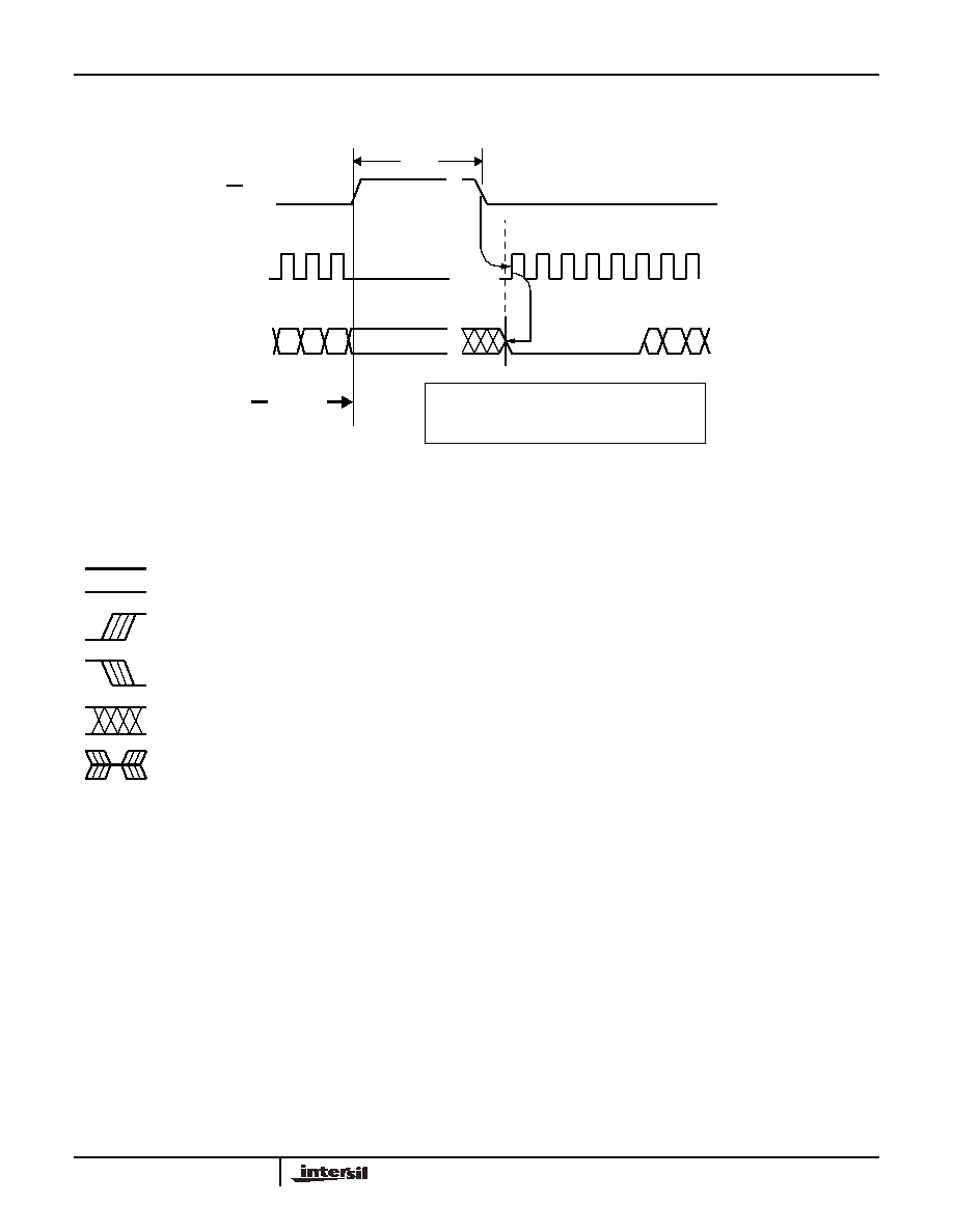
CS vs. RESET Timing
RESET Output Timing
SYMBOL
PARAMETER
MIN
TYP
MAX
UNIT
V
TRIP
Reset trip point voltage, X5083PT-4.5A (Note 6)
Reset trip point voltage, X5083PT
Reset trip point voltage, X5083PT-2.7A
Reset trip point voltage, X5083PT-2.7
4.5
4.25
2.85
2.55
4.63
4.38
2.93
2.63
4.75
4.5
3.00
2.7
V
t
PURST
Power-up reset time out
100
200
280
ms
t
RPD
(Note 5)
V
CC
detect to reset/output
500
ns
t
F
(Note 5)
V
CC
fall time
0.1
ns
t
R
(Note 5)
V
CC
rise time
0.1
ns
V
RVALID
Reset valid V
CC
1
V
NOTES:
5. This parameter is periodically sampled and not 100% tested.
6. PT = Package/Temperature
CS
t
CST
RESET
t
WDO
t
RST
t
WDO
t
RST
RESET Output Timing
SYMBOL
PARAMETER
MIN
TYP
MAX
UNIT
t
WDO
Watchdog time out period,
WD1 = 1, WD0 = 1(default)
WD1 = 1, WD0 = 0
WD1 = 0, WD0 = 1
WD1 = 0, WD0 = 0
100
450
1
OFF
200
600
1.4
300
800
2
ms
ms
sec
t
CST
CS pulse width to reset the watchdog
400
ns
t
RST
Reset time out
100
200
300
ms
X5083

17
FN8127.2
September 16, 2005
V
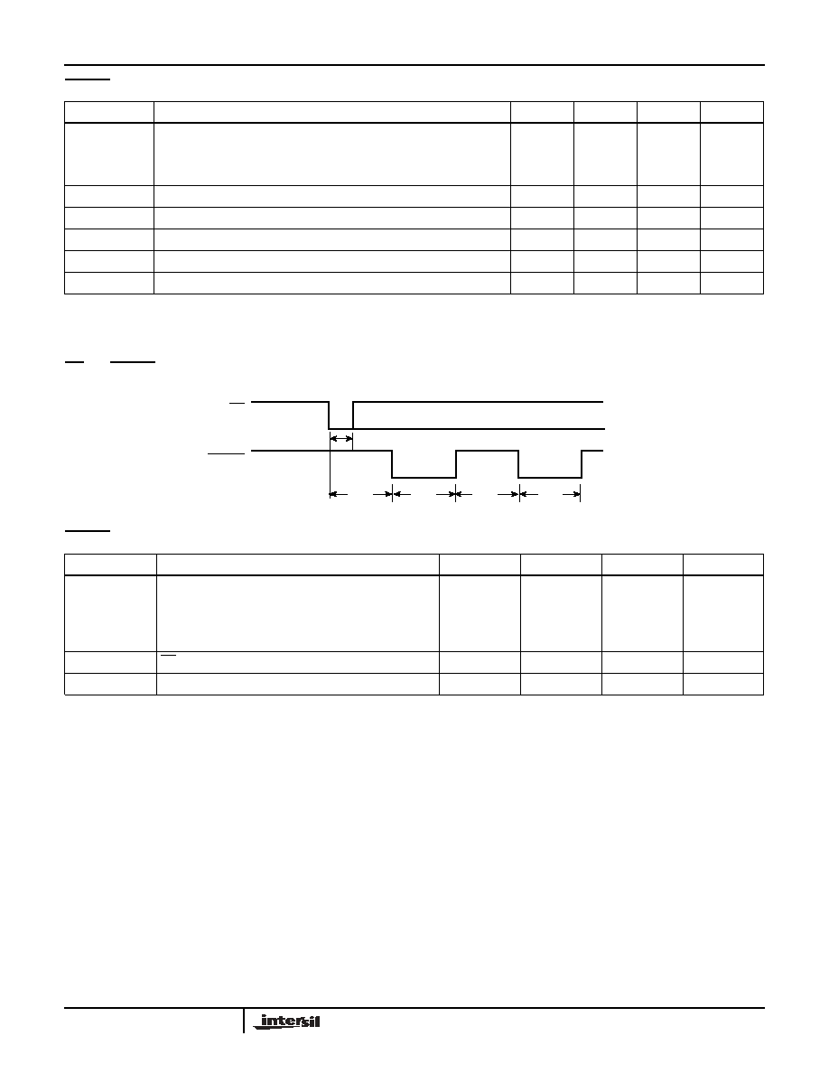
TRIP
Programming Timing Diagram
SCK
SI
CS
0001h (set)
V
CC
(V
TRIP
)
V
PE
t
TSU
t
THD
t
VPH
t
VPS
V
P
V
TRIP
t
RP
t
VPO
t
PCS
02h
06h
0003h (reset)
WREN
Write
Addr.
00
Data
V
TRIP
Programming Parameters
PARAMETER
DESCRIPTION
MIN
MAX
UNIT
t
VPS
V
TRIP
program enable voltage setup time
1
µs
t
VPH
V
TRIP
program enable voltage hold time
1
µs
t
PCS
V
TRIP
programming CS inactive time
1
µs
t
TSU
V
TRIP
setup time
1
µs
t
THD
V
TRIP
hold (stable) time
10
ms
t
WC
V
TRIP
write cycle time
10
ms
t
VPO
V
TRIP
program enable voltage off time (between successive adjustments)
0
µs
t
RP
V
TRIP
program recovery period (between successive adjustments)
10
ms
V
P
Programming voltage
15
18
V
V
TRAN
V
TRIP
programmed voltage range
2.0
5.0
V
V
tv
V
TRIP
program variation after programming (0-75∞C). (programmed at 25∞C)
-25
+25
mV
NOTES:
7. V
TRIP
programming parameters are periodically sampled and are not 100% tested.
8. For custom V
TRIP
settings, Contact Factory.
X5083
18
FN8127.2
September 16, 2005
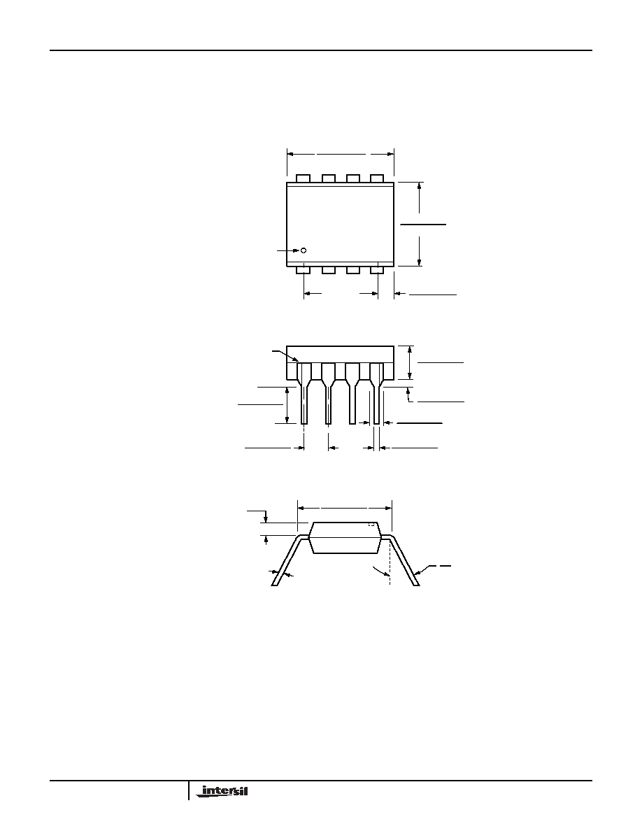
Packaging Information
NOTE:
1. ALL DIMENSIONS IN INCHES (IN PARENTHESES IN MILLIMETERS)
2. PACKAGE DIMENSIONS EXCLUDE MOLDING FLASH
0.020 (0.51)
0.016 (0.41)
0.150 (3.81)
0.125 (3.18)
0.110 (2.79)
0.090 (2.29)
0.430 (10.92)
0.360 (9.14)
0.300
(7.62) Ref.
Pin 1 Index
0.145 (3.68)
0.128 (3.25)
0.025 (0.64)
0.015 (0.38)
Pin 1
Seating
0.065 (1.65)
0.045 (1.14)
0.260 (6.60)
0.240 (6.10)
0.060 (1.52)
0.020 (0.51)
Typ. 0.010 (0.25)
0∞
15∞
8-Lead Plastic Dual In-Line Package Type P
Half Shoulder Width On
All End Pins Optional
.073 (1.84)
Max.
0.325 (8.25)
0.300 (7.62)
Plane
X5083
19
FN8127.2
September 16, 2005
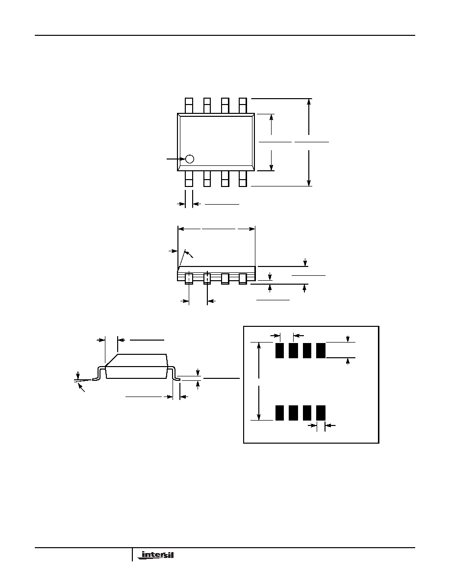
Packaging Information
0.150 (3.80)
0.158 (4.00)
0.228 (5.80)
0.244 (6.20)
0.014 (0.35)
0.019 (0.49)
Pin 1
Pin 1 Index
0.010 (0.25)
0.020 (0.50)
0.050 (1.27)
0.188 (4.78)
0.197 (5.00)
0.004 (0.19)
0.010 (0.25)
0.053 (1.35)
0.069 (1.75)
(4X) 7∞
0.016 (0.410)
0.037 (0.937)
0.0075 (0.19)
0.010 (0.25)
0∞ - 8∞
X 45∞
8-Lead Plastic Small Outline Gull Wing Package Type S
NOTE: ALL DIMENSIONS IN INCHES (IN PARENTHESES IN MILLIMETERS)
0.250"
0.050" Typical
0.050"
Typical
0.030"
Typical
8 Places
FOOTPRINT
X5083
20
All Intersil U.S. products are manufactured, assembled and tested utilizing ISO9000 quality systems.
Intersil Corporation's quality certifications can be viewed at www.intersil.com/design/quality
Intersil products are sold by description only. Intersil Corporation reserves the right to make changes in circuit design, software and/or specifications at any time without
notice. Accordingly, the reader is cautioned to verify that data sheets are current before placing orders. Information furnished by Intersil is believed to be accurate and
reliable. However, no responsibility is assumed by Intersil or its subsidiaries for its use; nor for any infringements of patents or other rights of third parties which may result
from its use. No license is granted by implication or otherwise under any patent or patent rights of Intersil or its subsidiaries.
For information regarding Intersil Corporation and its products, see www.intersil.com
FN8127.2
September 16, 2005
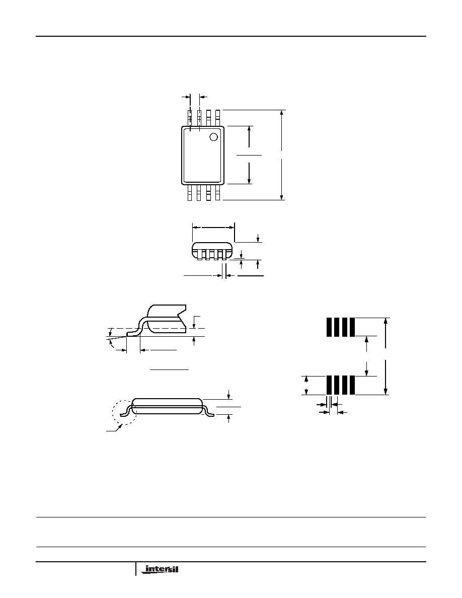
Packaging Information
NOTE: ALL DIMENSIONS IN INCHES (IN PARENTHESES IN MILLIMETERS)
8-Lead Plastic, TSSOP, Package Type V
See Detail "A"
.031 (.80)
.041 (1.05)
.169 (4.3)
.177 (4.5)
.252 (6.4) BSC
.025 (.65) BSC
.114 (2.9)
.122 (3.1)
.002 (.05)
.006 (.15)
.047 (1.20)
.0075 (.19)
.0118 (.30)
0∞ - 8∞
.010 (.25)
.019 (.50)
.029 (.75)
Gage Plane
Seating Plane
Detail A (20X)
(4.16) (7.72)
(1.78)
(0.42)
(0.65)
All Measurements Are Typical
X5083