REV 1.2.6 4/22/04
1 of 10
www.xicor.com
FEATURES
∑ Output Voltage: 2.500V
∑ Absolute Initial Accuracy Options:
±0.5mV & ±1.0mV
∑ Ultra Low Power Supply Current: 500nA
∑ Low Temperature Coefficient options:
3, 5 & 10ppm/∞C
∑ 10 mA Source & Sink Current Capability
∑ 10 ppm/1000hrs Long Term Stability
∑ Supply Voltage Range: 4.5V to 6.5V
∑ 5kV ESD (Human Body Model)
∑ Standard Package: SOIC-8
∑ Temp Range: -40∞C to +85∞C
DESCRIPTION
The X60008-25 FGATM voltage references are very
high precision analog voltage references fabricated in
Xicor's proprietary Floating Gate Analog technology,
which achieves superior levels of performance when
compared to conventional band gap, buried zener, or
X
FET
TM technologies.
FGATM voltage references feature very high initial
accuracy, very low temperature coefficient, excellent
long term stability, low noise and excellent line and
load regulation, at the lowest power consumption
currently available. These voltage references enable
advanced applications for precision industrial &
portable systems operating at significantly higher
accuracy and lower power levels than can be achieved
with conventional technologies.
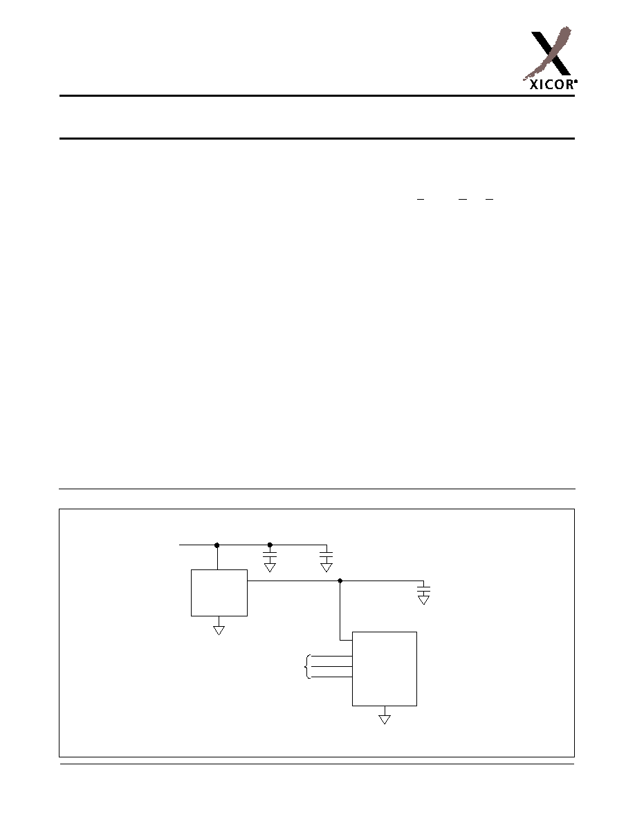
TYPICAL APPLICATION
APPLICATIONS
∑ High Resolution A/Ds & D/As
∑ Precision Current Sources
∑ Smart sensors
∑ Digital Meters
∑ Precision Regulators
∑ Strain Gage Bridges
∑ Calibration Systems
∑ Precision Oscillators
∑ Threshold Detectors
∑ V-F Converters
∑ Battery Management Systems
∑ Servo Systems
V
IN
= +5.0V
0.1µF
Serial
Bus
V
IN
V
OUT
GND
X60008-25
Enable
SCK
SDAT
A/D Converter
16 to 24-bit
REF IN
10µF
0.001µF
(
*
)
(
*
)
Also see Figure 3 in Applications Information
Precision 2.5V FGATM Voltage Reference
X60008B-25
X60008C-25
X60008D-25

2 of 10
REV 1.2.6 4/22/04
www.xicor.com
X60008B-25, X60008C-25, X60008D-25
PACKAGE DIAGRAM
PIN CONFIGURATIONS
ORDERING INFORMATION
Pin Name
Description
GND
Ground Connection
V
IN
Power Supply Input Connection
V
OUT
Voltage Reference Output Connection
DNC
Do Not Connect; Internal Connection ≠ Must Be Left Floating
1
2
3
4
8
7
6
5
SOIC
V
IN
DNC
GND
X60008-XX
DNC
DNC
V
OUT
DNC
GND
Logo
Device Part Number
60008 = Standard
Grade
B = ±0.5 mV, 3 ppm/∞C
C = ±0.5 mV, 5 ppm/∞C
D = ±1.0 mV, 10 ppm/∞C
Temperature Range
I = -40∞C to +85∞C
Package
S8 = 8 lead SOIC
V
OUT
Option
25 = 2.500V
X
60008
C
I
S8 ≠ 25

3 of 10
REV 1.2.6 4/22/04
www.xicor.com
X60008B-25, X60008C-25, X60008D-25
ABSOLUTE MAXIMUM RATINGS
Storage Temperature Range ................. ≠65∞C to +125∞C
Max Voltage Applied V
IN
to Gnd ............... ≠0.5V to +6.5V
Max Voltage Applied V
OUT
to Gnd
(*)
......... ≠0.5V to +3.5V
Voltage on "DNC" pins ......... No connections permitted to
these pins.
Lead Temperature, soldering
(*)
............................+ 225∞C
(*) note: maximum duration = 10 seconds
RECOMMENDED OPERATING CONDITIONS
COMMENT
Absolute Maximum Ratings are limits which may result
in impaired reliability and/or permanent damage to the
device. These are stress ratings provided for informa-
tion only and functional operation of the device at
these or any other conditions beyond those indicated
in the operational sections of this specification are not
implied.
For guaranteed specifications and test conditions, see
Electrical Characteristics.
The guaranteed specifications apply only for the test
conditions listed. Some performance characteristics
may degrade when the device is not operated under
the listed test conditions.
Temperature
Min.
Max.
Industrial
≠40∞C
+85∞C
ELECTRICAL CHARACTERISTICS
(Operating Conditions: V
IN
= 5.0V, I
OUT
= 0mA, C
OUT
= 0.001µF, T
A
= -40 to +85∞C unless otherwise specified.)
Note:
1. Over the specified temperature range. Temperature coefficient is measured by the box method whereby the change in V
OUT
is
divided by the temperature range; in this case, -40∞C to +85∞C = 125∞C.
2. Thermal Hysteresis is the change in V
OUT
created by package stress @ T
A
= 25∞C after temperature cycling. V
OUT
is read initially at
T
A
= 25∞C; the X60008 is then cycled between Hot (85∞C) and Cold (-40∞C) before a second V
OUT
measurement is taken at 25∞C.
The deviation between the initial V
OUT
reading and the second V
OUT
reading is then expressed in ppm.
3. Guaranteed by device characterization and/or correlation to other device tests.
Symbol
Parameter
Conditions
Min
Typ
Max
Units
V
OUT
Output Voltage
2.500
V
V
OA
V
OUT
Accuracy
X60008B-25
X60008C-25
X60008D-25
T
A
= 25∞C
-0.50
-0.50
-1.00
+0.50
+0.50
+1.00
mV
I
IN
Supply Current
500
800
nA
V
IN
Input Voltage Range
4.5
6.5
V
TC V
OUT
Output Voltage
Temperature Coefficient
(1)
X60008B-25
X60008C-25
X60008D-25
3
5
10
ppm/
∞
C
V
OUT
/
V
IN
Line Regulation
+4.5V
V
IN
+6.5V
100
µ
V/V
V
OUT
/
I
OUT
Load Regulation
0mA
I
SOURCE
10mA
-10mA
I
SINK
0mA
10
20
40
80
µ
V/mA
V
OUT
/
t
Long Term Stability
T
A
= 25∞C
10
ppm/
1000Hrs
V
OUT
/
T
A
Thermal Hysteresis
(2)
T = -40
∞
C to +85
∞
C
50
ppm
I
SC
Short Circuit Current
(3)
T
A
= 25∞C
50
80
mA
V
N
Output Voltage Noise
0.1Hz to 10Hz
30
µ
V
pp
4 of 10
REV 1.2.6 4/22/04
www.xicor.com
X60008B-25, X60008C-25, X60008D-25
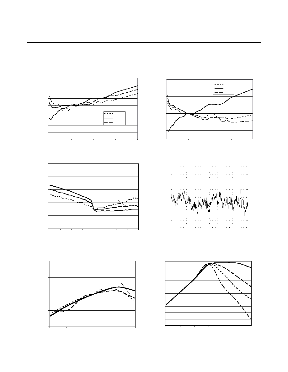
TYPICAL PERFORMANCE CHARACTERISTIC CURVES
(V
IN
= 5.0V, I
OUT
= 0mA, T
A
= 25∞C unless otherwise specified)
LINE REGULATION
LINE REGULATION
LOAD REGULATION
-0.3
-0.2
-0.1
0.0
0.1
0.2
0.3
0.4
0.5
0.6
0.7
-20
-15
-10
-5
0
5
10
15
20
SINKING
TEMPERATURE (
∞C)
SOURCING
I
OUT
(mA)
0.1Hz to 10Hz V
OUT
NOISE
1 Sec/div
10
µ
V/div
Band Pass Filter with 1 zero at .1Hz and 2 poles at 10 Hz
DELTA V
O
(
µ
V)
DELTA V
OUT
(mV)
V
OUT
(V)
(normailized to V
IN
= 5.00V)
V
OUT
(V)
(normailized to 2.5V at V
IN
= 5V)
V
IN
(V)
V
IN
(V)
+25
∞C -40∞C
+85
∞C
2.498
2.499
2.5
2.501
2.502
-40
-15
10
35
60
85
320nA
520nA
690nA
V
OUT
vs TEMPERATURE
Normalized to 25
∞C
-100
-90
-80
-70
-60
-50
-40
-30
-20
-10
0
1
10
100
1000
10000
100000
1000000
No Load
1nF Load
10nF
Load
100nF Load
FREQUENCY (Hz)
PSRR vs CAP Load
PSRR (dB)
4.5
5
5.5
6
6.5
-40
∞C
+25
∞C
+85
∞C
4.5
5
5.5
6
6.5
310nA
520nA
690nA
-100
-80
-60
-40
-20
0
20
40
60
80
2.49994
2.49996
2.49998
2.5
2.50002
2.50004
2.50006
2.50008
5 of 10
REV 1.2.6 4/22/04
www.xicor.com
X60008B-25, X60008C-25, X60008D-25
TYPICAL PERFORMANCE CHARACTERISTIC CURVES
(V
IN
= 5.0V, I
OUT
= 0mA, T
A
= 25∞C unless otherwise specified)
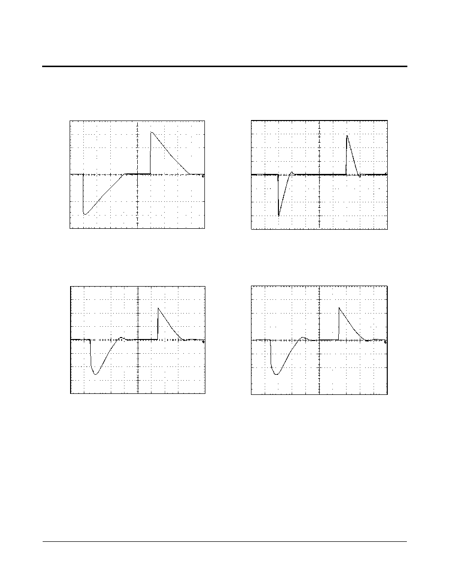
10mA LOAD TRANSIENT RESPONSE
500mV/DIV
C
L
= .001
µF
IN
= -10mA
I
I
I
I
IN
= +10mA
1mS/DIV
50
µA LOAD TRANSIENT RESPONSE
100mV/DIV
500
µSEC/DIV
C
L
= .001
µF
IN
= -50
µA
IN
= +50
µA
LINE TRANSIENT RESPONSE
LINE TRANSIENT RESPONSE
200mV/DIV
500
µSEC/DIV
200mV/DIV
500
µSEC/DIV
C
L
= 0
C
L
= .001
µF
V
IN
= -500mV
V
IN
= +500mV
V
IN
= -500mV
V
IN
= +500mV
X60008B-25, X60008C-25, X60008D-25
6 of 10
REV 1.2.6 4/22/04
www.xicor.com
TYPICAL PERFORMANCE CHARACTERISTIC CURVES
(V
IN
= 5.0V, I
OUT
= 0mA, T
A
= 25∞C unless otherwise specified)
0
50
100
150
200
250
300
100
100
10
1000
10000
100000
no Load
1nF Load
10nF Load
100nF Load
0
1
2
3
4
5
6
-1
1
3
5
7
9
11
V
IN
V
OUT
Z
OUT
vs FREQUENCY
FREQUENCY (Hz)
Z
OUT
(
)
I
IN
(nA)
V
IN
(V)
I
IN
vs V
IN
I
IN
(nA)
V
IN
(V)
I
IN
vs V
IN
TURN-ON TIME
V
IN
& V
OUT
(V)
TIME (mSec)
0
100
200
300
400
500
600
700
800
4.5
5
5.5
6
6.5
3 units representative of I
IN
Range
480
500
520
540
560
580
600
4.5
5
5.5
6
6.5
-40∞C
+25∞C
+85∞C

7 of 10
REV 1.2.6 4/22/04
www.xicor.com
X60008B-25, X60008C-25, X60008D-25
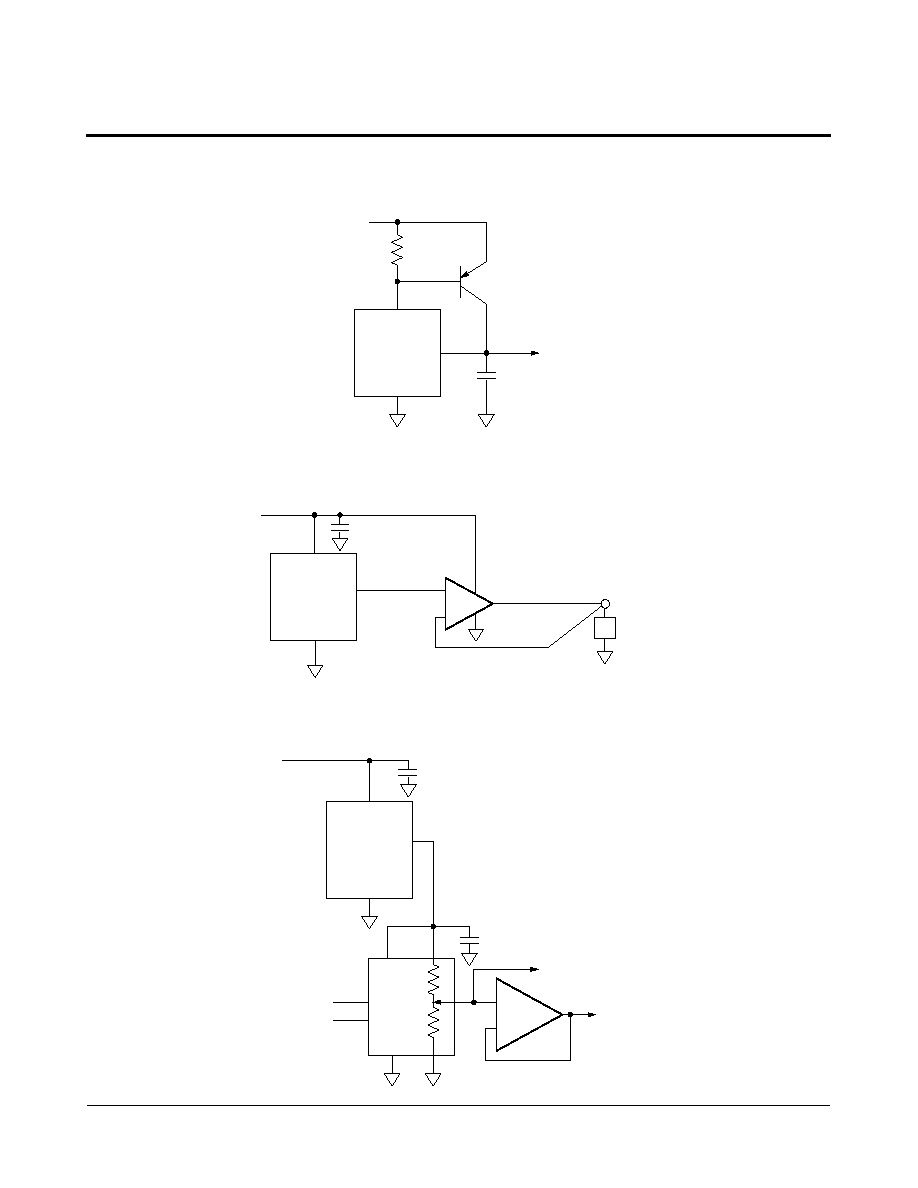
APPLICATIONS INFORMATION
FGA Technology
The X60008 series of voltage references use the float-
ing gate technology to create references with very low
drift and supply current. Essentially the charge stored
on a floating gate cell is set precisely in manufacturing.
The reference voltage output itself is a buffered version
of the floating gate voltage. The resulting reference
device has excellent characteristics which are unique
in the industry: very low temperature drift, high initial
accuracy, and almost zero supply current. Also, the ref-
erence voltage itself is not limited by voltage bandgaps
or zener settings, so a wide range of reference volt-
ages can be programmed (standard voltage settings
are provided, but customer-specific voltages are avail-
able).
The process used for these reference devices is a
floating gate CMOS process, and the amplifier circuitry
uses CMOS transistors for amplifier and output transis-
tor circuitry. While providing excellent accuracy, there
are limitations in output noise level and load regulation
due to the MOS device characteristics. These limita-
tions are addressed with circuit techniques discussed
in other sections.
Nanopower Operation
Reference devices achieve their highest accuracy
when powered up continuously, and after initial stabili-
zation has taken place. This drift can be eliminated by
leaving the power on continuously.
The X60008 is the first high precision voltage refer-
ence with ultra low power consumption that makes it
possible to leave power on continuously in battery
operated circuits. The X60008 consumes extremely
low supply current due to the proprietary FGA technol-
ogy. Supply current at room temperature is typically
500nA which is 1 to 2 orders of magnitude lower than
competitive devices. Application circuits using battery
power will benefit greatly from having an accurate, sta-
ble reference which essentially presents no load to the
battery.
In particular, battery powered data converter circuits
that would normally require the entire circuit to be dis-
abled when not in use can remain powered up
between conversions as shown in figure 1. Data acqui-
sition circuits providing 12 to 24 bits of accuracy can
operate with the reference device continuously biased
with no power penalty, providing the highest accuracy
and lowest possible long term drift.
Other reference devices consuming higher supply cur-
rents will need to be disabled in between conversions
to conserve battery capacity. Absolute accuracy will
suffer as the device is biased and requires time to set-
tle to its final value, or, may not actually settle to a final
value as power on time may be short.
Figure 1.
Board mounting Considerations
For applications requiring the highest accuracy, board
mounting location should be reviewed. Placing the
device in areas subject to slight twisting can cause
degradation of the accuracy of the reference voltage
due to die stresses. It is normally best to place the
device near the edge of a board, or the shortest side,
as the axis of bending is most limited at that location.
Obviously mounting the device on flexprint or
extremely thin PC material will likewise cause loss of
reference accuracy.
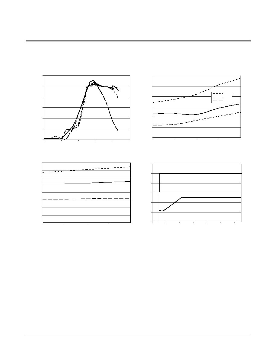
Noise Performance and Reduction:
The output noise voltage in a 0.1Hz to 10Hz bandwidth
is typically 30µVp-p. This is shown in the plot in the
Typical Performance Curves. The noise measurement
is made with a bandpass filter made of a 1 pole high-
pass filter with a corner frequency at .1Hz and a 2-pole
low-pass filter with a corner frequency at 12.6Hz to
create a filter with a 9.9Hz bandwidth. Noise in the
10KHz to 1MHz bandwidth is approximately 400µVp-p
with no capacitance on the output, as shown in Fig. 2
below. These noise measurements are made with a 2
decade bandpass filter made of a 1 pole high-pass
V
IN
= 4.5V to 6.5V
0.001µF
Serial
Bus
V
IN
V
OUT
GND
X60008-25
REF IN
Enable
SCK
SDAT
A/D Converter
12 to 24-bit
0.01µF
10µF

X60008B-25, X60008C-25, X60008D-25
8 of 10
REV 1.2.6 4/22/04
www.xicor.com
filter with a corner frequency at 1/10 of the center
frequency and 1-pole low-pass filter with a corner
frequency at 10 times the center frequency. Figure 2
also shows the noise in the 10KHz to 1MHz band can
be reduced to about 50µVp-p using a .001µF capacitor
on the output. Noise in the 1KHz to 100KHz band can
be further reduced using a 0.1µF capacitor on the
output, but noise in the 1Hz to 100Hz band increases
due to instability of the very low power amplifier with a
0.1µF capacitance load. For load capacitances above
.001µF the noise reduction network shown in fig. 3 is
recommended. This network reduces noise sig-
nificantly over the full bandwidth. As shown in fig. 2,
noise is reduced to less than 40µVp-p from 1Hz to
1MHz using this network with a .01µF capacitor and a
2Kohm resistor in series with a 10µF capacitor.
Figure 2.
Figure 3.
Turn-On Time
The X60008 devices have ultra-low supply current and
thus the time to bias up internal circuitry to final values
will be longer than with higher power references. Nor-
mal turn-on time is typically 7ms. This is shown in the
graph, Figure 4. Since devices can vary in supply cur-
rent down to 300nA, turn-on time can last up to about
12ms. Care should be taken in system design to
include this delay before measurements or conver-
sions are started.
Figure 4.
Temperature Coefficient
The limits stated for temperature coefficient (tempco)
are governed by the method of measurement. The
overwhelming standard for specifying the temperature
drift of a reference is to measure the reference voltage
at two temperatures, take the total variation, (V
HIGH
≠
V
LOW
), and divide by the temperature extremes of
measurement (T
HIGH
≠ T
LOW
). The result is divided by
the nominal reference voltage (at T=25∞C) and multi-
plied by 10
6
to yield ppm/∞C. This is the "Box" method.
CL = 0
CL = .001µF
CL = .1µF
CL = .01µF & 10µF + 2kohm
400
350
300
250
200
150
100
50
0
1
10
100
1000
10000
100000
X60008-25 NOISE REDUCTION
NOISE VOLTAGE (µVp-p)
V
IN
= 6.5V
V
IN
V
O
GND
X60008-25
.01µF
10µF
2K
.1µF
10µF
0
1
2
3
4
5
6
-1
1
3
5
7
9
690 nA
520 nA
320 nA
V
IN
V
OUT
X60008 TURN-ON TIME (25
∞C)
TIME (mSec)
V
IN
& V
OUT
(V)
9 of 10
REV 1.2.6 4/22/04
www.xicor.com
X60008B-25, X60008C-25, X60008D-25
TYPICAL APPLICATION CIRCUITS
Precision 2.5V, 50mA Reference.
V
IN
= 5.2V to 6.5V
2N2905
2.5V/50mA
0.009µF
V
IN
V
OUT
GND
X60008-25
Kelvin Sensed Load
0.1µF
5.0V
V
IN
V
OUT
GND
X60008-25
V
OUT
Sense
Load
R = 200
+
≠
V
IN
V
OUT
X60008-25
GND
4.5V to 6.5V
0.1µF
0.01µF
V
OUT
+
≠
V
CC
R
H
R
L
X9119
V
SS
SDA
SCL
2-Wire Bus
V
OUT
(buffered)
2.5V Full Scale Low-Drift 10-bit Adjustable Voltage Source
Characteristics subject to change without notice.
10 of 10
LIMITED WARRANTY
Devices sold by Xicor, Inc. are covered by the warranty and patent indemnification provisions appearing in its Terms of Sale only. Xicor, Inc. makes no warranty,
express, statutory, implied, or by description regarding the information set forth herein or regarding the freedom of the described devices from patent infringement.
Xicor, Inc. makes no warranty of merchantability or fitness for any purpose. Xicor, Inc. reserves the right to discontinue production and change specifications and prices
at any time and without notice.
Xicor, Inc. assumes no responsibility for the use of any circuitry other than circuitry embodied in a Xicor, Inc. product. No other circuits, patents, or licenses are implied.
TRADEMARK DISCLAIMER:
Xicor and the Xicor logo are registered trademarks of Xicor, Inc. AutoStore, Direct Write, Block Lock, SerialFlash, MPS, BiasLock and XDCP are also trademarks of
Xicor, Inc. All others belong to their respective owners.
U.S. PATENTS
Xicor products are covered by one or more of the following U.S. Patents: 4,326,134; 4,393,481; 4,404,475; 4,450,402; 4,486,769; 4,488,060; 4,520,461; 4,533,846;
4,599,706; 4,617,652; 4,668,932; 4,752,912; 4,829,482; 4,874,967; 4,883,976; 4,980,859; 5,012,132; 5,003,197; 5,023,694; 5,084,667; 5,153,880; 5,153,691;
5,161,137; 5,219,774; 5,270,927; 5,324,676; 5,434,396; 5,544,103; 5,587,573; 5,835,409; 5,977,585. Foreign patents and additional patents pending.
LIFE RELATED POLICY
In situations where semiconductor component failure may endanger life, system designers using this product should design the system with appropriate error detection
and correction, redundancy and back-up features to prevent such an occurrence.
Xicor's products are not authorized for use in critical components in life support devices or systems.
1. Life support devices or systems are devices or systems which, (a) are intended for surgical implant into the body, or (b) support or sustain life, and whose failure to
perform, when properly used in accordance with instructions for use provided in the labeling, can be reasonably expected to result in a significant injury to the user.
2. A critical component is any component of a life support device or system whose failure to perform can be reasonably expected to cause the failure of the life
support device or system, or to affect its safety or effectiveness.
©Xicor, Inc. 2004 Patents Pending
REV 1.2.6 4/22/04
www.xicor.com
X60008B-25, X60008C-25, X60008D-25
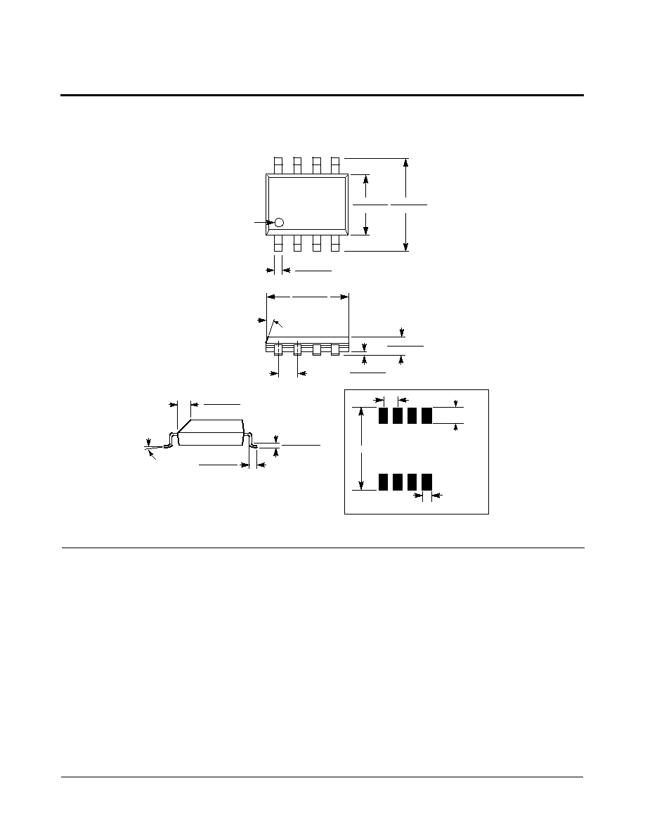
PACKAGING INFORMATION
0.150 (3.80)
0.158 (4.00)
0.228 (5.80)
0.244 (6.20)
0.014 (0.35)
0.019 (0.49)
Pin 1
Pin 1 Index
0.010 (0.25)
0.020 (0.50)
0.050 (1.27)
0.188 (4.78)
0.197 (5.00)
0.004 (0.19)
0.010 (0.25)
0.053 (1.35)
0.069 (1.75)
(4X) 7∞
0.016 (0.410)
0.037 (0.937)
0.0075 (0.19)
0.010 (0.25)
0∞ - 8∞
X 45∞
8-Lead Plastic, SOIC, Package Code S8
NOTE: ALL DIMENSIONS IN INCHES (IN PARENTHESES IN MILLIMETERS)
0.250"
0.050" Typical
0.050"
Typical
0.030"
Typical
8 Places
FOOTPRINT