 | –≠–ª–µ–∫—Ç—Ä–æ–Ω–Ω—ã–π –∫–æ–º–ø–æ–Ω–µ–Ω—Ç: X60250 | –°–∫–∞—á–∞—Ç—å:  PDF PDF  ZIP ZIP |

1
Æ
FN8146.1
CAUTION: These devices are sensitive to electrostatic discharge; follow proper IC Handling Procedures.
1-888-INTERSIL or 1-888-468-3774
|
Intersil (and design) is a registered trademark of Intersil Americas Inc.
Copyright Intersil Americas Inc. 2005. All Rights Reserved
All other trademarks mentioned are the property of their respective owners.
X60250
Micro Power Programmable Voltage
Reference
FEATURES
∑ 1.25V 1.0%, 20ppm/∞C Tempco Reference
∑ Adjustable to ±0.25% Over the 0 to 1.25V Range
∑ 8 bit, 100k
XDCP on-chip
∑ Programmable Resolution of 4.9mV (255 steps)
∑ Extra Matched 100k
Resistor Available for
Increased Resolution Over a Smaller Range
∑ 2.7V to 5.5V Supply Range
∑ 2-Wire Interface for Programming Reference
Setting
∑ Low Supply Current: 12µA in Normal Mode
∑ 8-pin TSSOP Package
∑ Programmable Reference
∑ NV Memory
∑ Pb-Free Plus Anneal Available (RoHS Compliant)
PROGRAMMABLE VOLTAGE
REFERENCE APPLICATIONS
∑ Sensor Bias
∑ Variable DAC reference
∑ Linear Voltage Regulators
∑ DC/DC converters
∑ Voltage comparators
∑ Motor controllers
∑ Amplifier biasing
DESCRIPTION
The Intersil X60250 combines a temperature
compensated voltage reference with a Intersil Digitally
Controlled Potentiometer (XDCP) to provide a precision
adjustable reference with a range of 0.0V to 1.25V. The
device includes a serial bus interface to enable in-circuit
programming of the reference voltage.
The XDCP contains a resistor chain with 255 taps to
provide 8 bits of digital adjustment to the reference
voltage. Non-volatile storage retains the digital wiper
setting, for permanent reference programming. An
additional matched 100k
resistor is available to
increase resolution of the output voltage while retaining
accuracy.
IC BLOCK DIAGRAM
V
CC
V
REFOUT
SCL
SDA
GND
V
REFL
V
OUT
R
1
100K
100k
1.25V
Reference
Serial
Interface
EE
PROM
256 T
ap DC
P
Pwr On Recall
Digital Wiper
Control
Data Sheet
September 14, 2005
2
FN8146.1
September 14, 2005
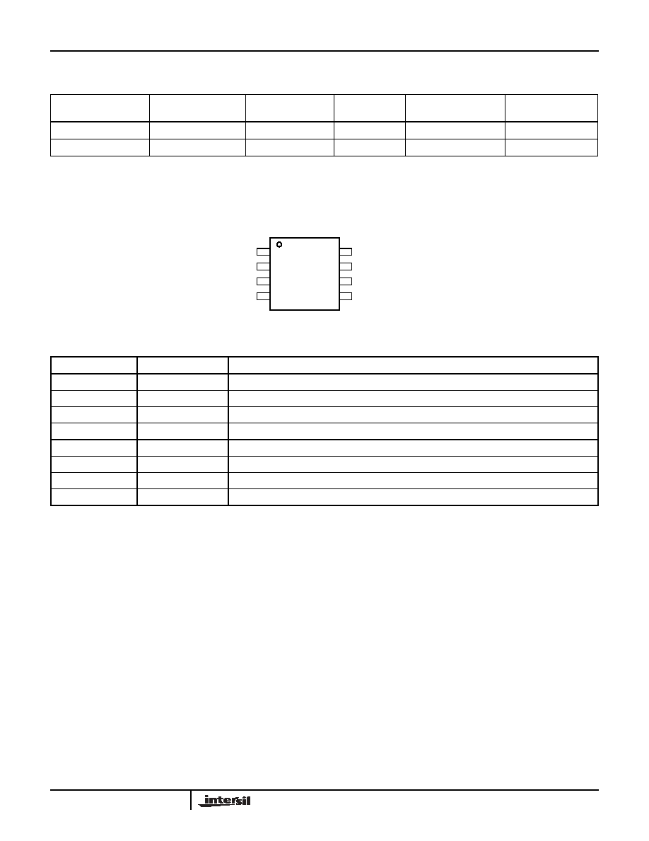
PIN CONFIGURATION
PIN ASSIGNMENTS
Ordering Information
PART NUMBER
PART MARKING
OUTPUT VOLTAGE
(V)
RESOLUTION
TEMP RANGE (∞C)
PACKAGE
X60250V8I
60250 I
1.250
8 bits
-40 to 85
8 Ld TSSOP
X60250V8IZ (Note)
60250I Z
1.250
8 bits
-40 to 85
8 Ld TSSOP (Pb-free)
NOTE: Intersil Pb-free plus anneal products employ special Pb-free material sets; molding compounds/die attach materials and 100% matte tin plate
termination finish, which are RoHS compliant and compatible with both SnPb and Pb-free soldering operations. Intersil Pb-free products are MSL
classified at Pb-free peak reflow temperatures that meet or exceed the Pb-free requirements of IPC/JEDEC J STD-020.
TSSOP
Symbol
Description
1
V
REFL
DCP and auxiliary resistor reference input
2
V
CC
Positive Power Supply
3
V
REFOUT
Bandgap Reference Output
4
V
OUT
DCP Wiper Output
5
R
1
Auxiliary resistor input
6
GND
Ground
7
SDA
Serial Data Input/Output
8
SCL
Serial Clock Input
TSSOP
V
REFL
V
CC
1
2
3
4
SDA
SCL
8
7
6
5
V
REFOUT
V
OUT
GND
R
1
X60250
3
FN8146.1
September 14, 2005
ABSOLUTE MAXIMUM RATINGS
Supply Voltage Range...................................-1V to 7V
Bias Temperature Range .................... -40∞C to +85∞C
Storage Temperature Range............. -65∞C to +150∞C
Voltage on V
REF(LOW)
pin .............................0V to V
CC
Voltage on all other pins ................-0.3V to V
CC
+0.3V
Lead temperature (soldering, 10 seconds)........ 300∞C
RECOMMENDED OPERATING CONDITIONS
COMMENTS
Absolute Maximum Ratings indicate limits beyond
which permanent damage to the device and impaired
reliability may occur. These are stress ratings provided
for information only and functional operation of the
device at these or any other conditions beyond those
indicated in the operational sections of this specification
are not implied.
For guaranteed specifications and test conditions, see
Electrical Characteristics.
The guaranteed specifications apply only for the test con-
ditions listed. Some performance characteristics may de-
grade when the device is not operated under the listed
test conditions.
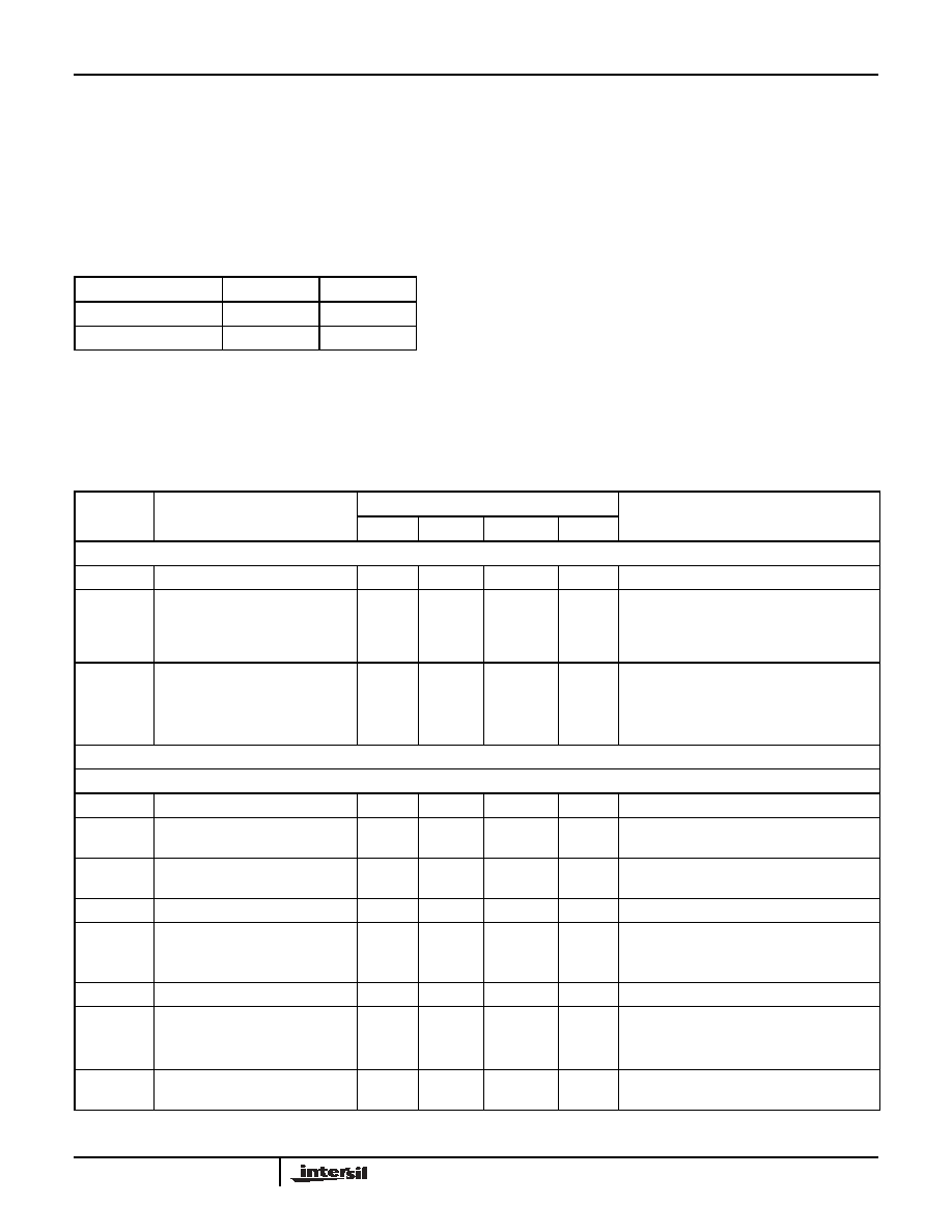
ELECTRICAL CHARACTERISTICS
(Over operating conditions unless otherwise specified. I
OUT
= 12.5 µA, R
1
= N/C (Floating).)
Min
Max
Temperature -40∞C
+85∞C
Supply Voltage
2.7V
5.5V
ANALOG PARAMETERS
Symbol
Parameter
Limits
Test Conditions
Min.
Typ.
(1)
Max.
Unit
Power Supply
V
CC
Supply Voltage Range
2.7
3.0
5.5
V
I
Q
Supply Current
V
CC
= 2.7V
V
CC
= 3V
V
CC
= 5.5V Write
15
20
60
µA
R
L
=0, V
REFL
, V
OUT
, R
AUX
= floating
I
Q(NV)
Non-Volatile Supply Current
V
CC
= 2.7V
V
CC
= 3V
V
CC
= 5.5V
600
1100
1300
µA
R
L
=0, V
REFL
, V
OUT
, R
AUX
= floating
Reference Output Voltage
DC Parameters
V
REFOUT
Output Voltage
1.237
1.250
1.263
V
T
A
= 25∞C
V
REFL
DCP and auxilliary resistor
reference input
GND
V
REFOUT
V
TCOref
Temperature coefficient of
V
REF
output voltage
20
70
ppm/∞C
(2, 5)
PSRR
Power Supply Rejection
55
66
dB
(6)
I
OUT
Output Current
Sourcing
Sinking
1
400
µA
(2)
R
OUT
Output Impedance
1
2.5
Given by R
OUT
= (
V
REF
/
I
OUT
)
(2)
I
SC
Short Circuit Current
Sourcing
Sinking
5
0
mA
At 5.5V
C
L
Load Capacitance
0.001
0.003
µF
Reference output stable for all CL up
to specifications
(2)
X60250

4
FN8146.1
September 14, 2005
DIGITAL PARAMETERS
EEPROM PARAMETERS (Erase at V
CC
= 5.0 V min, T = 25∞C)
CAPACITANCE
AC Parameters
V
N
Output Voltage Noise
100
200
µVP-P
µVRMS
0.1Hz to 10Hz
(2)
10Hz to 10kHz
(2)
Power-on Response
250
µs
1% Settling (2)
Line Ripple Rejection
60
dB
V
DD
= 3V ±100mV, f = 120 Hz
(2)
Reference DCP
Resolution
8
bits
R
TOT
End to end resistance
85
100
115
k
R
W
Wiper Resistance
V
CC
= 2.7V
V
CC
= 3V
600
5000
1200
(2)
Absolute Linearity (INL)
±0.2
LSB
Relative Linearity (DNL)
±0.1
LSB
R
TOT
Temperature Coeff.
±300
ppm/∞C
Ratiometric Temp. Coeff.
±20
ppm/∞C
R
AUX
(Auxiliary Resistor)
R
TOT
End to end resistance
85
100
115
k
R
TOT
Temperature Coeff.
±300
ppm/∞C R
L
=0, V
REFL
, V
OUT
, R
AUX
= floating
DCP Matching Tolerance
0.1
%
DCP Matching Temp. Coeff.
±20
ppm/∞C
Symbol
Parameter
Limits
Test Conditions
Min.
Typ.
(1)
Max.
Unit
I
LI
Input Leakage Current
2
µA
V
IN
= GND to V
CC
I
LO
Output Leakage Current
2
µA
V
OUT
= GND to V
CC
V
IL
Input Low Voltage
0
V
CC
x 0.2
V
V
IH
Input High Voltage
V
CC
x 0.7
V
CC
V
C
IN
Input Capacitance
5
pF
V
OL
Output Low Voltage
0
10
%V
DD
I
OL
= 100 µA
(2)
V
OH
Output High Voltage
90
100
%V
DD
I
OH
= 100 µA
(2)
C
L
Output Load
100
pF
(2)
Parameter
Min.
Units
Write Cycle Endurance
100,000
Cycles per bit
Symbol
Test
Max.
Units
Test Conditions
C
IN/OUT
Input/Output capacitance (SDA)
8
pF
V
OUT
= 0V
(2)
C
IN
Input capacitance (SCL)
6
pF
V
IN
= 0V
(2)
ANALOG PARAMETERS
(CONTINUED)
Symbol
Parameter
Limits
Test Conditions
Min.
Typ.
(1)
Max.
Unit
X60250

5
FN8146.1
September 14, 2005
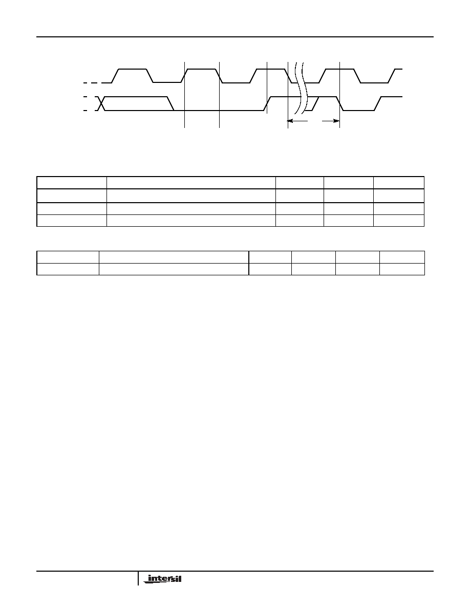
A.C. TEST CONDITIONS
AC SPECIFICATIONS
TIMING DIAGRAMS
Bus Timing
Input Pulse Levels
V
CC
x 0.1 to V
CC
x 0.9
Input rise and fall times
10ns
Input and output timing threshold level
V
CC
x 0.5
External load at pin SDA
2.3k
to V
CC
and 100 pF to V
SS
Symbol Parameter
Min.
Max.
Unit
f
SCL
SCL Clock Frequency
0
400
kHz
t
IN
Pulse width Suppression Time at inputs
(2)
50
ns
t
AA
SCL LOW to SDA Data Out Valid
(2)
0.1
0.9
µs
t
BUF
Time the bus must be free before a new transmission can start
(2)
1.3
µs
t
LOW
Clock LOW Time
1.3
µs
t
HIGH
Clock HIGH Time
0.6
µs
t
SU:STA
Start Condition Setup Time
0.6
µs
t
HD:STA
Start Condition Hold Time
0.6
µs
t
SU:DAT
Data In Setup Time
100
ns
t
HD:DAT
Data In Hold Time
0
µs
t
SU:STO
Stop Condition Setup Time
(2)
0.6
µs
t
DH
Data Output Hold Time
(2)
50
ns
t
R
SDA and SCL Rise Time
(2, 3)
20 +.1Cb
300
ns
t
F
SDA and SCL Fall Time
(2, 3)
20 +.1Cb
300
ns
Cb
Capacitive load for each bus line
(2, 3)
400
pF
t
SU:STO
t
HIGH
t
SU:STA
t
HD:STA
t
HD:DAT
t
SU:DAT
SCL
SDA IN
SDA OUT
t
F
t
LOW
t
HD:DAT
t
R
t
DH
t
AA
t
BUF
t
HD:STO
t
BUF
X60250
6
FN8146.1
September 14, 2005
WRITE CYCLE TIMING
POWER-UP TIMING
NONVOLATILE WRITE CYCLE TIMING
Notes: (1) Typical values are for T
A
= 25∞C and V
CC
= 3.0V
(2) This parameter is guaranteed by characterization.
(3) Cb = total capacitance of one bus line in pF.
(4) t
WC
is the time from a valid stop condition at the end of a write sequence to the end of the self-timed internal nonvolatile
write cycle. It is the minimum cycle time to be allowed for any nonvolatile write by the user, unless Acknowledge Polling is used.
(5) Over the specified temperature range. Temperature coefficient is measured by the box method whereby the change in
V
OUT
is divided by the temperature range; in this case, -40∞C to +85∞C = 125∞C. TCOref = [Max V(V
REF
) - Min V(V
REF
)]
◊
10
6
/ (1.25V
◊
125∞C)
SCL
SDA
t
WC
8th Bit of Last Byte
ACK
Stop
Condition
Start
Condition
Symbol Parameter
Min.
Max.
Unit
V
CC
/
t
V
CC
Power-up rate
(2)
0.2
50
V/ms
t
PUR
Time from Power-up to Read
(2)
1
ms
t
PUW
Time from Power-up to Write
(2)
5
ms
Symbol Parameter
Min.
Typ.
Max.
Unit
t
WC
Write Cycle Time
(4)
5
10
ms
X60250

7
FN8146.1
September 14, 2005
FUNCTIONAL DESCRIPTION
The X60250 combines a micropower precision reference
with an 8-bit, 256 tap digitally controlled 100k
potentiometer (DCP) which allows nonvolatile setting of
an output reference voltage. When normally configured
with the V
REFL
pin tied to ground, the device provides an
output range of 0V to 1.25V with 4.90mV resolution.
The device can also be configured with an optional
100k
series resistor to ground, which effectively halves
the output voltage range while doubling the resolution.
Grounding the R
1
pin while floating the V
REFL
pin places
the device in this mode. Output voltage setting accuracy
can be as high as 0.10% while permitting adjustment
from 0.625V to 1.25V (2.45mV resolution).
Reference Section
The reference is designed to provide an accurate, low
tempco voltage source while requiring less than 12µA
(typical) of supply current. This supply current is for the
reference section only. Keep in mind that the DCP will
increase supply current draw by VREF/RTOTAL
(typically 1.25/100k or 12.5µA). The total current drawn
by the adjustable reference circuit will be less than 25µA
(typically).
The reference output has a typical impedance of 1
and
can provide up to 400µA of load current. It is intended to
drive the resistive load of the DCP, which is a minimum
of 85k
, but can also be used to drive off chip circuitry
provided the loading does not exceed the 400µA
maximum. Also, highly capacitive loads can make the
reference oscillate, so no more than 2000pF should be
placed directly on the output of the V
REFOUT
pin.
The reference output produces about 200µV RMS of
noise (10kHz bandwidth) due to its micropower design.
This is easily reduced in normal applications, as shown in
the applications section for optimizing circuits for
reducing output noise levels.
DCP Section
The 256 tap DCP has an 8-bit nonvolatile wiper control
register which controls which tap is selected. The
register is changed by performing a serial data write to its
address (0h, see Serial Interface section). The resulting
wiper position will produce an output voltage at V
OUT
,
depending on whether the DCP V
REFL
is grounded or the
R
1
pin is grounded. The wiper consists of CMOS
transistors and has a finite resistance, typically 600
at
V
CC
= 5V (this parameter increases with decreasing
V
CC
). The wiper resistance will produce errors in
reference circuits due to I-R drops if current flows
through the wiper. However, typically these circuits will
have the wiper connected to a high impedance
comparator or amplifier input which results in very small
wiper currents and thus only a small output voltage error.
If the X60250 is used with the wiper connected to V
REFL
to produce a current source, care must be taken to avoid
exceeding the maximum output current of the reference
(typically 400µA).
Power-Up considerations
The X60250 contains EEPROM nonvolatile storage cells
which are recalled during power-up. This recall process
works best with power supply (V
CC
) ramping that is
monotonic and free of excessive glitches (<100mV
disturbances give best results). The ramp rate spec
should be adhered to, although the most sensitive part of
recall is between V
CC
= 1.0V and 2.5V. Effort should be
made to make sure the device receives a power-up ramp
between those voltage levels that meet the ramp rate
spec and have no glitches.
Recall of the stored wiper position happens in < 1ms
from V
CC
reaching 2.5V. Note that any excursions of V
CC
below 2.5V, although temporary, can cause the wiper to
be loaded with the midpoint value (80h) until V
CC
recovers to its normal voltage.
Register Organization
There are 2 nonvolatile registers and 1 volatile register
available for storage and recall via the serial bus. They
contain the current wiper position, a general purpose
data register and a status register.
The wiper register is nonvolatile and is at address 0h and
contains 8 bits, with the 00h setting corresponding to the
tap position nearest V
REFL
, and the FFh setting nearest
to V
REFOUT
.
The general purpose register is nonvolatile and is at
address 1h, and contains 8 bits for use as scratchpad
memory or serial number information.
The Status register is volatile and is at address 7h. It has
one active bit, D3, which is the WEL bit. This bit must be
set to 1 berfore any nonvolatile writes are performed to
the other registers. See the register information on the
next page.
X60250

8
FN8146.1
September 14, 2005
X60250 REGISTER BIT MAP
REGISTER DESCRIPTIONS
REGISTER 0 (NONVOLATILE)
This register is used to hold the DCP wiper position, which is given by:
REGISTER 1 (NONVOLATILE)
This 8 bit register is used for general storage such as date code, temp setting, etc.
STATUS REGISTER
Addr
D7
D6
D5
D4
D3
D2
D1
D0
0
D7
(MSB)
D6
D5
D4
D3
D2
D1
D0 (LSB)
1
D7
(MSB)
D6
D5
D4
D3
D2
D1
D0 (LSB)
7
0
0
0
0
WEL
0
0
0
Reg
Nonvolatile
Description
0
1
7
Y
Y
N
V
OUT
wiper setting
General Purpose data storage register
Status register
Bit
Value
Description
D - D4
D3
D2 - D0
0
0 - 1
0
Must remain 0
WEL bit
Must be programmed to "1" for Reg 0 or 1 EEPROM
write. When accessing, only WEL bit may be changed
Must remain 0
V
OUT
V
REF
Code
255
---------------
◊
=
(with
V
REFL
= GND)
X60250

9
FN8146.1
September 14, 2005
X60250 BUS INTERFACE INFORMATION
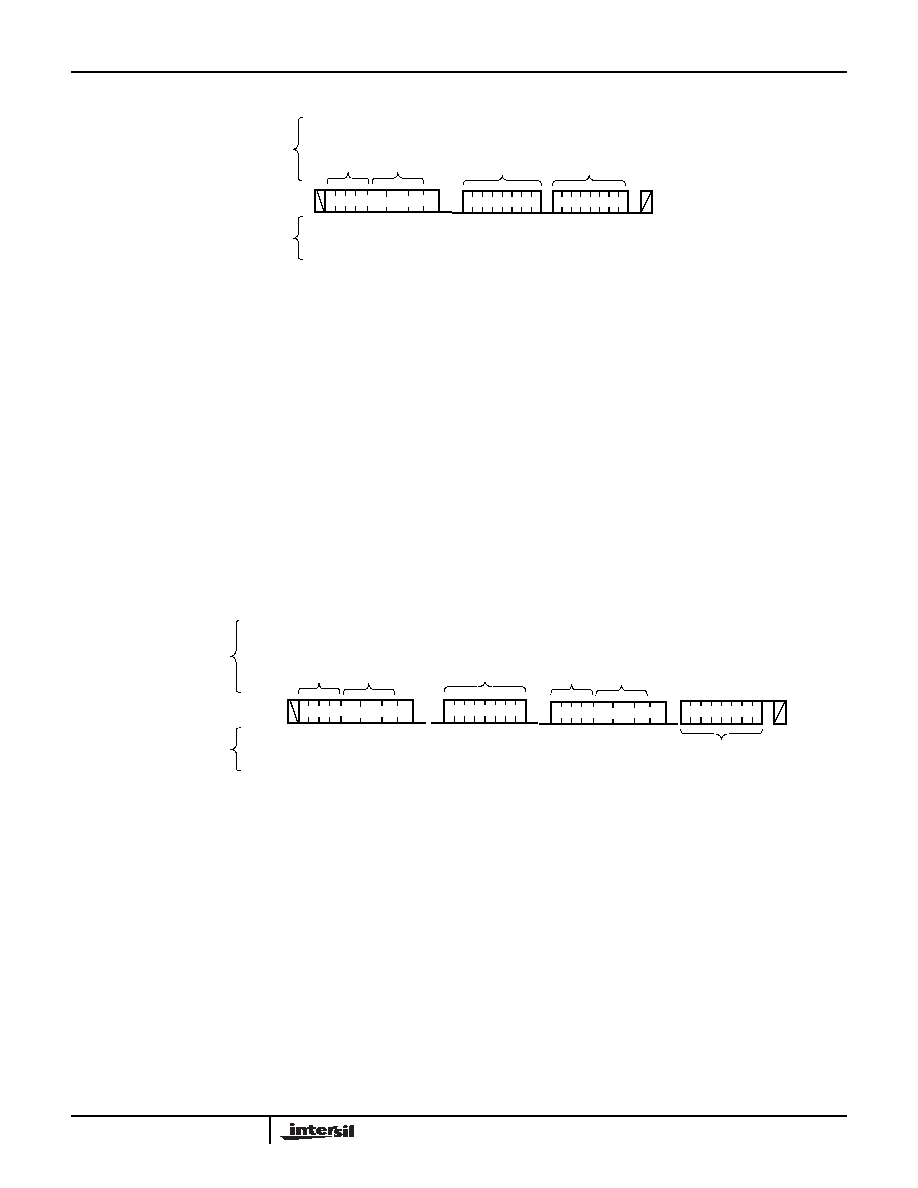
Figure 1. Slave Address, Word Address, and Data Bytes - Write Mode
Figure 2. Slave Address, Word Address, and Data Bytes - Read Mode
Slave Address Byte
Byte 0
D7
D6
D5
D2
D4
D3
D1
D0
A0
A7
A2
A4
A3
A1
Data Byte
Byte 2
A6
A5
0
1
0
0
1
0 / 1
0
0
Device Identifier
Byte Address
Byte 1
Slave Address*
Slave Address Byte
Byte 0
D7
D6
D5
D2
D4
D3
D1
D0
D0
D7
D2
D4
D3
D1
Data Byte
Byte 2
D6
D5
0
1
0
0
1
0 / 1
1
0
Device Identifier
Data Byte
Byte 1
Slave Address*
X60250

10
FN8146.1
September 14, 2005
X60250 BUS INTERFACE INFORMATION
Slave Address, Address Byte, and Data Byte
The byte communication format for the serial bus is
shown in Figure 1 on the previous page. The first byte,
BYTE 0, defines the device identifier, 0101 in the upper
half; and the device slave address in the low half of the
byte. The slave address is set to 0. The next byte,
BYTE 1, is the Address Byte. The Address Byte
identifies a unique address for the Status or Control
Registers as shown in the Register Descriptions table.
The following byte, Byte 2, is the byte used for READ
and WRITE operations.
Start Condition
All commands are preceded by the start condition, which
is a HIGH to LOW transition of SDA when SCL is HIGH.
The device continuously monitors the SDA and SCL
lines for the start condition and will not respond to any
command until this condition has been met. On power-
up, the SCL pin must be brought LOW prior to the
START condition. See Figure 3.
Stop Condition
All communications must be terminated by a stop
condition, which is a LOW to HIGH transition of SDA
when SCL is HIGH followed by a HIGH to LOW
transistion on SCL. After going LOW, SCL can stay LOW
or return to HIGH. See Figure 3.
Acknowledge
Acknowledge is a software convention used to indicate
successful data transfer. The transmitting device, either
master or slave, will release the bus after transmitting
eight bits. During the ninth clock cycle, the receiver will
pull the SDA line LOW to acknowledge that it received
the eight bits of data. Refer to Figure 4. The device will
respond with an acknowledge after recognition of a start
condition and if the correct Device Identifier and Select
bits are contained in the Slave Address Byte. If a write
operation is selected, the device will respond with an
acknowledge after the receipt of each subsequent eight
bit word. The device will acknowledge all incoming data
and address bytes, except for:
≠ The Slave Address Byte when the Device Identifier
and/or Select bits are incorrect
≠ The 2nd Data Byte of a Status Register Write Oper-
ation (only 1 data byte is allowed)
Pin Descriptions
V
REFOUT
Reference voltage output. The 1.25V bandgap
reference output (V
REF
) is available at this pin for
application to other circuits. Maximum output current is
400µA. The V
REFOUT
pin also connects to the Rh
terminal of the 256-tap DCP.
V
OUT
DCP Wiper Output. This pin functions as the wiper of the
DCP, and can be used as a variable voltage source for
voltages between GND and V
REF
. Since it is connected
to the DCP resistor, any loads on this pin must be high
impedance for best performance.
R
1
Auxiliary Resistor Input. The R
1
pin is connected to one
end of a 100k
resistor (R
1
) which closely matches the
DCP resistance. The other end of R
1
is tied to the R
REFL
terminal of the DCP. When R
1
is grounded and V
REFL
is
left open, the output voltage range of V
OUT
will be from
V
REF
/2 to V
REF
, and the effective resolution (mV/step) of
the Reference control is doubled. R
1
should be left open
if not used.
GND
This pin is common for the V
REF
output and for control
signal inputs.
SDA
Serial Data Input/Output. Bidirectional pin used for serial
data transfer. As an output, it is open drain and may be
wire-ored with any number of open drain or open
collector outputs. A pullup resistor is required and the
value is dependent on the speed of the serial data bus
and the number of outputs tied together.
SCL
Serial Clock Input. Accepts a clock signal for clocking
serial data into and out of the device.
V
REFL
DCP and Auxiliary Resistor Input. This pin is connected
to one end of the 256-tap DCP, and also to one end of
the 100k
auxiliary resistor. When connected to ground,
V
OUT
range will be from 0V to V
REF
. When left open
and R
1
is connected to ground, the voltage at this pin will
be from V
REF
/2 to V
REF
.
X60250
11
FN8146.1
September 14, 2005
V
CC
Positive Power Supply. Connect to a voltage supply in
the range of 2.7V < V
CC
< 5.5V, with minimum noise and
ripple. For best performance, bypass with a 0.1µF
capacitor to ground.
Figure 3. Valid Start and Stop Conditions
Figure 4. Acknowledge Response From Receiver
Figure 5. Valid Data Changes on the SDA Bus
SCL
SDA
Start
Stop
SCL from
Master
Data Output
from Transmitter
Data Output
from Receiver
8
1
9
Start
Acknowledge
SCL
SDA
Data Stable
Data Change
Data Stable
X60250
12
FN8146.1
September 14, 2005
Figure 6. Byte Write Sequence
Byte Write
For a write operation, the device requires the Slave
Address Byte and the Word Address Bytes. This gives
the master access to any one of the words in the array.
Upon receipt of each address byte, the X60250 responds
with an acknowledge. After receiving the address bytes
the X60250 awaits the eight bits of data. After receiving
the 8 data bits, the X60250 again responds with an
acknowledge. The master then terminates the transfer by
generating a stop condition. The X60250 then begins an
internal write cycle of the data to the nonvolatile memory.
During the internal write cycle, the device inputs are
disabled, so the device will not respond to any requests
from the master. The SDA output is at high impedance.
See Figure 6.
A write to a protected block of memory is ignored, but will
still receive an acknowledge. At the end of the write
command, the X60250 will not initiate an internal write
cycle, and will continue to okay commands.
Stops and Write Modes
Stop conditions that terminate write operations must be
sent by the master after sending at least 1 full data byte
and its associated ACK signal. If a stop is issued in the
middle of a data byte, or before 1 full data byte + ACK is
sent, then the X60250 resets itself without performing the
write. The contents of the array are not affected.
Figure 7. Random Address Read Sequence
Random Address Read
Random read operation allows the master to access any
location in the X60250. Prior to issuing the Slave
Address Byte, the master must first perform a "dummy"
write operation.
The master issues the start condition and the slave
address byte, receives an acknowledge, then issues the
word address bytes. After acknowledging receipt of each
word address byte, the master immediately issues
another start condition and the slave address byte. This
is followed by an acknowledge from the device and then
by the eight bit data word. The master terminates the
read operation by not responding with an acknowledge
and then issuing a stop condition. Refer to Figure 7 for
the address, acknowledge, and data transfer sequence.
In a similar operation called "Set Current Address," the
device sets the address if a stop is issued instead of the
second start shown in Figure 7. The X60250 then goes
into standby mode after the stop and all bus activity will
be ignored until a start is detected. This operation loads
the new address into the address counter. The next
Current Address Read operation will read from the newly
loaded address. This operation could be useful if the
master knows the next address it needs to read, but is
not ready for the data.
S
t
a
r
t
S
t
o
p
Data
A
C
K
A
C
K
SDA Bus
Signals From
The Slave
Signals from
the Master
0
A
C
K
Byte
Address 0
0/1
0
0
0
1
0
1
Slave
Address*
Device
ID
*Note: The X60250 will respond to either 000 or 001 slave addresses.
A
C
K
S
t
a
r
t
S
t
o
p
Data
S
t
a
r
t
SDA Bus
Signals from
the Slave
Signals from the
Master
Byte
Address 0
A
C
K
Slave
Address
0
0/1
0
0
0
1
0
1
Device
ID
A
C
K
Slave
Address
1
0
0
0
0
1
0
1
Device
ID
X60250
13
FN8146.1
September 14, 2005
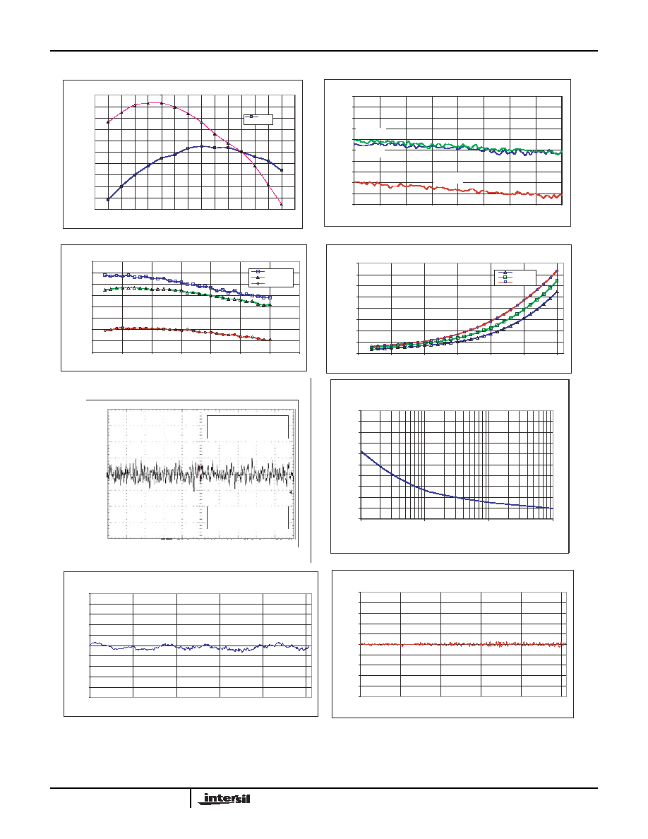
TYPICAL PERFORMANCE CHARACTERISTIC CURVES
Icc vs Vcc
10.00E-6
15.00E-6
20.00E-6
25.00E-6
30.00E-6
35.00E-6
40.00E-6
45.00E-6
50.00E-6
2.50
3.00
3.50
4.00
4.50
5.00
5.50
Vcc (V)
Icc (A)
Icc (-40C)
Icc (25C)
Icc (85C)
VRefout vs Temperature (2 representative units)
1.24620
1.24670
1.24720
1.24770
1.24820
1.24870
1.24920
1.24970
1.25020
1.25070
1.25120
-50
-40
-30
-20
-10
0
10
20
30
40
50
60
70
80
90
100
Temperature (C)
VRefout (V)
Refout
R f
t
VRefout vs Vcc
1.249E+0
1.250E+0
1.251E+0
1.252E+0
1.253E+0
1.254E+0
1.255E+0
1.256E+0
1.257E+0
2.50
3.00
3.50
4.00
4.50
5.00
5.50
6.00
Vcc (V)
VRefout (V)
Refout (-40C)
Refout (25C)
Refout (85C)
Vref Output Voltage Noise, 0.1Hz to 10Hz
Filter = 1 zero at 0.1Hz
2 poles at 10Hz
Vertical = 50
µ
V/div
Horizontal = 1 sec/div
INL
-0.50
-0.40
-0.30
-0.20
-0.10
0.00
0.10
0.20
0.30
0.40
0.50
0
50
100
150
200
250
Tap Position
ERROR (LSB)
DNL
-0.50
-0.40
-0.30
-0.20
-0.10
0.00
0.10
0.20
0.30
0.40
0.50
0
50
100
150
200
250
Tap Position
ERROR (LSB)
VREF Output Noise Spectrum
0
1
2
3
4
5
6
7
8
9
10
10
100
1000
10000
Frequency
Noise, uV/rt*H
z
I
REFOOUT
vs V
REFOUT
1.2450
1.2460
1.2470
1.2480
1.2490
1.2500
1.2510
1.2520
1.2530
1.2540
1.2550
0.00
0.10
0.20
0.30
0.40
0.50
0.60
0.70
0.80
I
REFOUT
(mA)
V
REFOUT
(V
)
+25 deg C
-40 deg C
+85 deg C
X60250
14
FN8146.1
September 14, 2005
TYPICAL PERFORMANCE CHARACTERISTIC CURVES (Continued)
APPLICATIONS INFORMATION
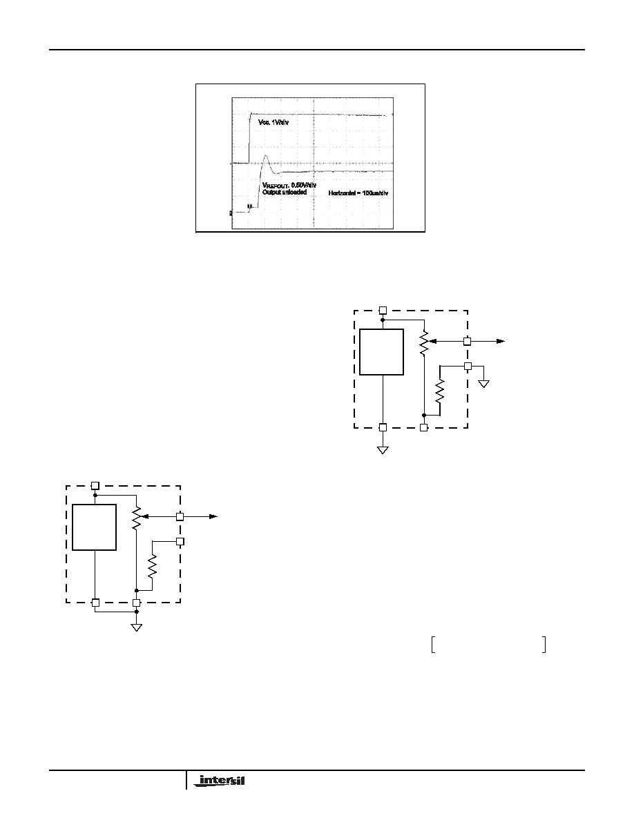
Standard Reference configurations
Figure 8 shows the device connections to produce a 0
to 1.250V adjustable reference with 8 bits of resolution.
V
REFL
will be grounded in this case. Figure 9 has
device connections to produce a 0.625V to 1.250V
reference with 8 bits of resolution, with R
1
grounded.
This configuration effectively doubles the output voltage
control resolution, increasing the accuracy of the
desired reference output voltage. Since the auxiliary
resistor is matched to the DCP resistor, temperature
drift is minimized.
Figure 8. Standard Configuration
Figure 9. Using Auxilliary Resistor
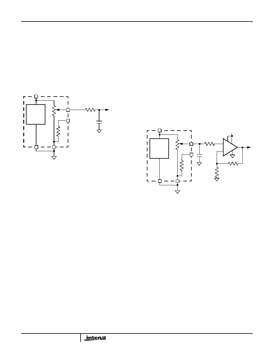
Reducing Output Noise
The output noise voltage of the reference is typically
200µV rms in the 10kHz bandwidth. An advantage of the
adjustable reference configuration is the ease in filtering
this noise. Simply adding a capacitor to the V
OUT
pin will
produce a single pole filter with a corner frequency of:
R
DCP
will vary with tap position and wiper resistance. If
the approximate tap position of the DCP is known, it can
be used to calculate this resistance as follows:
For example, with V
CC
= 5V, tap # = 127 (corresponding
to V
OUT
= 0.623V), C
FILTER
= 0.1µF, using typical values:
Power On Settling Time
V
REFOUT
1.25V
Reference
100K
100K
V
REFL
GND
R
1
V
OUT
Adjusted
Reference
Voltage
0.0 to 1.25V Range
V
REFOUT
1.25V
Reference
100K
100K
V
REFL
GND
R
1
V
OUT
0.625V to 1.25V
Range
F
CORNER
1
2
---
◊
R
DCP
C
FILTER
◊
◊
=
R
DCP
255 tapw
≠
255
------------------------------
R
TOTAL
tapw
255
-------------- R
TOTAL
◊
||
R
WIPER
+
◊
=
#
#
R
DCP
25K 0.6K
+
25.6k
=
=
F
CORNER
62Hz
=
X60250
15
FN8146.1
September 14, 2005
Since this is a single pole rolloff, the actual noise
bandwidth is 1.57 times this, or 97Hz. This should
reduce typical output noise to about 45µV rms. Note that
if the wiper is set to the highest tap positon (tap# = 255)
to give a V
OUT
of 1.25V, the resulting R
DCP
= R
WIPER
or
600
, and the filter bandwidth will now be 2.6kHz,
increasing noise significantly. If tap positions near
V
REFOUT
will be used, then a series resistor R
OUT
should
be added to better control noise bandwidth.
Figure 10. Reducing Output Noise
Higher Reference Voltages
If a reference voltage higher than 1.25V is required, then
an opamp can be added to amplify the V
OUT
voltage.
There are many micropower opamps available, such as
the LMV341, which can produce an output at very close
to either supply rail. Figure 11 shows a circuit for a 0V to
5.0V adjustable reference, which has 8 bits of control.
Note that if the auxiliary resistor is connected to ground
instead of V
REFL
, then the output voltage range will be
2.5V to 5.0V, but resolution will double. Total current
draw from that circuit will be 156µA (typically, with
V
OUT
= 5V) including reference and opamp circuitry.
Note that due to V
CC
supply variations, the output may
not span up to 5.00V which would result in missing codes
at the top end of the DCP range.
Figure 11. Increasing Reference Output Voltage
R
1
C
FILTER
R
OUT
V
REFOUT
1.25V
Reference
100K
100K
V
REFL
GND
V
OUT
(optional)
Filtered
Reference
Voltage
≠
+
R
1
+5V
0 to
4
2
LMV341
100K
33K
6
1
3
5
20K
C
FILTER
V
REFOUT
1.25V
Reference
100K
100K
V
REFL
GND
5.0V
X60250

16
All Intersil U.S. products are manufactured, assembled and tested utilizing ISO9000 quality systems.
Intersil Corporation's quality certifications can be viewed at www.intersil.com/design/quality
Intersil products are sold by description only. Intersil Corporation reserves the right to make changes in circuit design, software and/or specifications at any time without
notice. Accordingly, the reader is cautioned to verify that data sheets are current before placing orders. Information furnished by Intersil is believed to be accurate and
reliable. However, no responsibility is assumed by Intersil or its subsidiaries for its use; nor for any infringements of patents or other rights of third parties which may result
from its use. No license is granted by implication or otherwise under any patent or patent rights of Intersil or its subsidiaries.
For information regarding Intersil Corporation and its products, see www.intersil.com
FN8146.1
September 14, 2005
PACKAGING INFORMATION
8-Lead Plastic, TSSOP, Package Code V8
See Detail "A"
.031 (.80)
.041 (1.05)
.169 (4.3)
.177 (4.5)
.252 (6.4) BSC
.025 (.65) BSC
.114 (2.9)
.122 (3.1)
.002 (.05)
.006 (.15)
.041 (1.05)
.0075 (.19)
.0118 (.30)
0∞ - 8∞
.010 (.25)
.019 (.50)
.029 (.75)
Gage Plane
Seating Plane
Detail A (20X)
(4.16) (7.72)
(1.78)
(0.42)
(0.65)
All Measurements Are Typical
X60250