1
Æ
FN8147.0
CAUTION: These devices are sensitive to electrostatic discharge; follow proper IC Handling Procedures.
1-888-INTERSIL or 1-888-352-6832
|
Intersil (and design) is a registered trademark of Intersil Americas Inc.
Copyright Intersil Americas Inc. 2005. All Rights Reserved
All other trademarks mentioned are the property of their respective owners.
X79000, X79001, X79002
NV DAC with Selectable Output Range
and Memory
FEATURES
∑ 12-Bit Resolution
∑ Selectable full scale and zero scale voltages
∑ Optional External full scale and zero scale
references
∑ Programmable, non-volatile DAC initial value
register
∑ Optional UP/DOWN interface
∑ Guaranteed Monotonic Operation, <0.5LSB DNL
∑ Buffered Output Option
∑ Integrated Voltage Reference Option
∑ Voltage Reference Output (1.21V) Option
∑ 6 µs settling time, full scale
∑ SPI interface, 5MHz
∑ Up to 5 slave Address Pins
∑ Power-up recall and ready output
∑ 56 Bytes of general purpose EEPROM
∑ Asynchronous clear pin and control bit
∑ V
CC
= 5V ±10%
∑ 20-lead TSSOP
∑ NV DAC
DESCRIPTION
The X79000 is a family of Single Channel Non-Volatile
(NV) Digital-to-Analog Converters with integrated
voltage reference, configurable output buffer, general
purpose EEPROM, and selectable full scale and zero
offset voltages.
The X79000 series implements an SPI serial bus
interface with slave address identification allowing up
to 32 devices on some options. The full scale and
zero scale voltages and the DAC initial value register
can be set via the SPI bus interface. Optional pins
are provided for Up/Down style interface allowing for
increment and decrement of the DAC register in 1, 4,
or 16 steps at a time.
A Power-on Recall circuit is implemented to keep the
DAC output at high impedance on power-up and to load
an initial user defined value from non-volatile memory. A
power-up ready signal is provided to alert the system to
begin operations.
Additional general purpose non-volatile memory (56
Bytes) is provided for curve-fit profile setting, signal
conditioning parameters, or device and system
indentification.
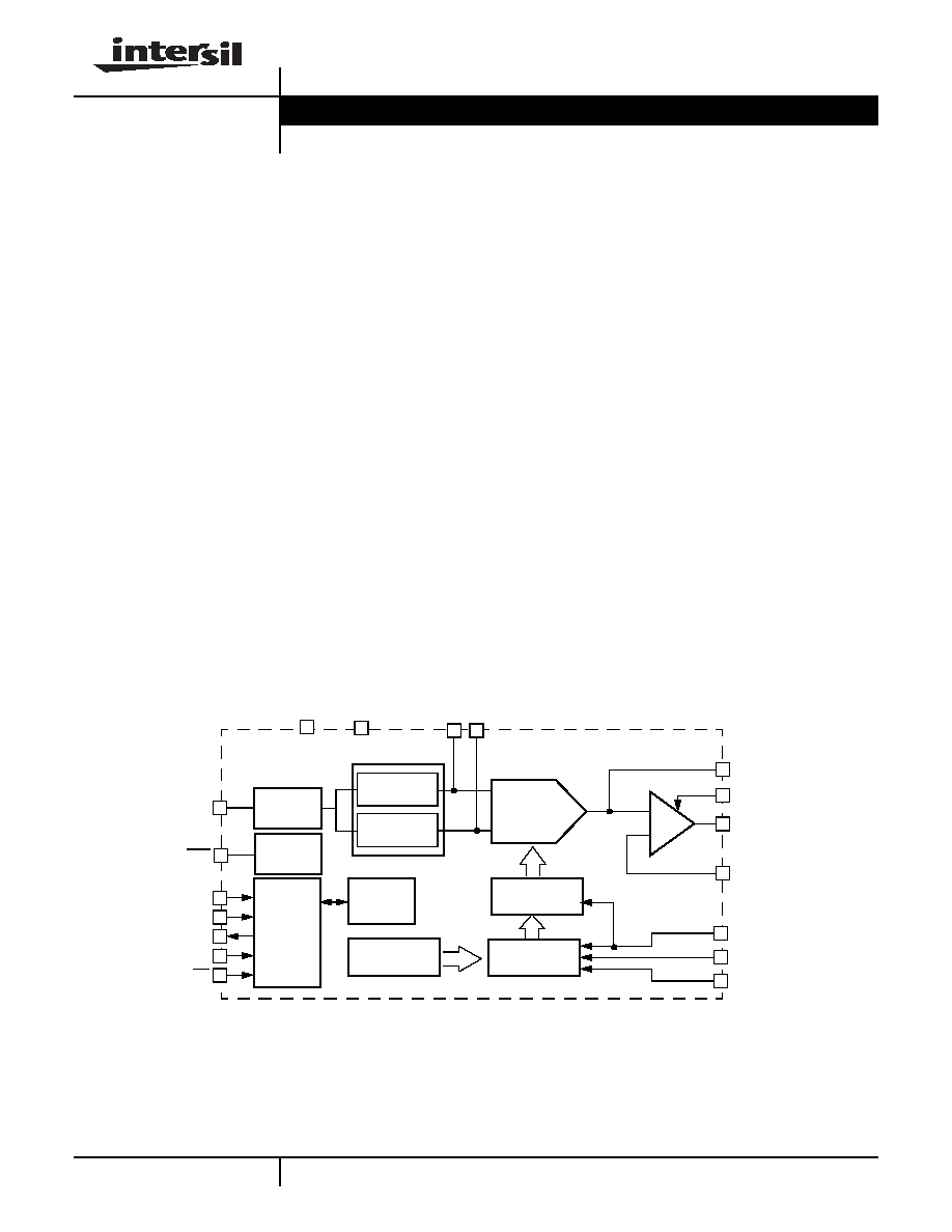
X79000 FUNCTIONAL DIAGRAM
Voltage
Reference
Variable Gain
& Level Shift
Variable Gain
& Level Shift
DAC
Core
+
≠
Vout
OE
Vbuf
VFB
Power-up
Logic
Serial
Interface
and
Control
Logic
Vref
RDY
A[2:0]
SCK
SO
SI
CS
General
DAC Register
DAC Shift
DAC Initial
Register
Value Register
CLR
UP
DOWN
Purpose
EEPROM
Vcc
Vss
VH VL
Data Sheet
March 17, 2005
2
FN8147.0
March 17, 2005
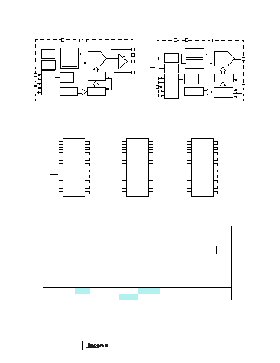
X79001 / X79002 FUNCTIONAL DIAGRAM
PIN CONFIGURATION
Variable Gain
& Level Shift
Variable Gain
& Level Shift
DAC
Core
+
≠
Vout
OE
Vbuf
VFB
Power-up
Logic
Serial
Interface
and
Control
Logic
RDY
A[5:0]
SCK
SO
SI
CS
General
DAC Register
DAC Shift
DAC Initial
Register
Value Register
CLR
Purpose
EEPROM
Vcc
Vss
VH VL
Vout
UP
CLR
DOWN
DAC
Core
X79002
X79001
DAC Initial
Voltage
Reference
Variable Gain
& Level Shift
Variable Gain
& Level Shift
Power-up
Logic
Serial
Interface
and
Control
Logic
Vref
RDY
A[4:0]
SCK
SO
SI
CS
General
DAC Register
DAC Shift
Register
Value Register
Purpose
EEPROM
Vcc
Vss
VH VL
Voltage
Reference
SCK
A0
A1
A2
SI
CS
CLR
V
CC
VH
VL
X79000
X79001
X79002
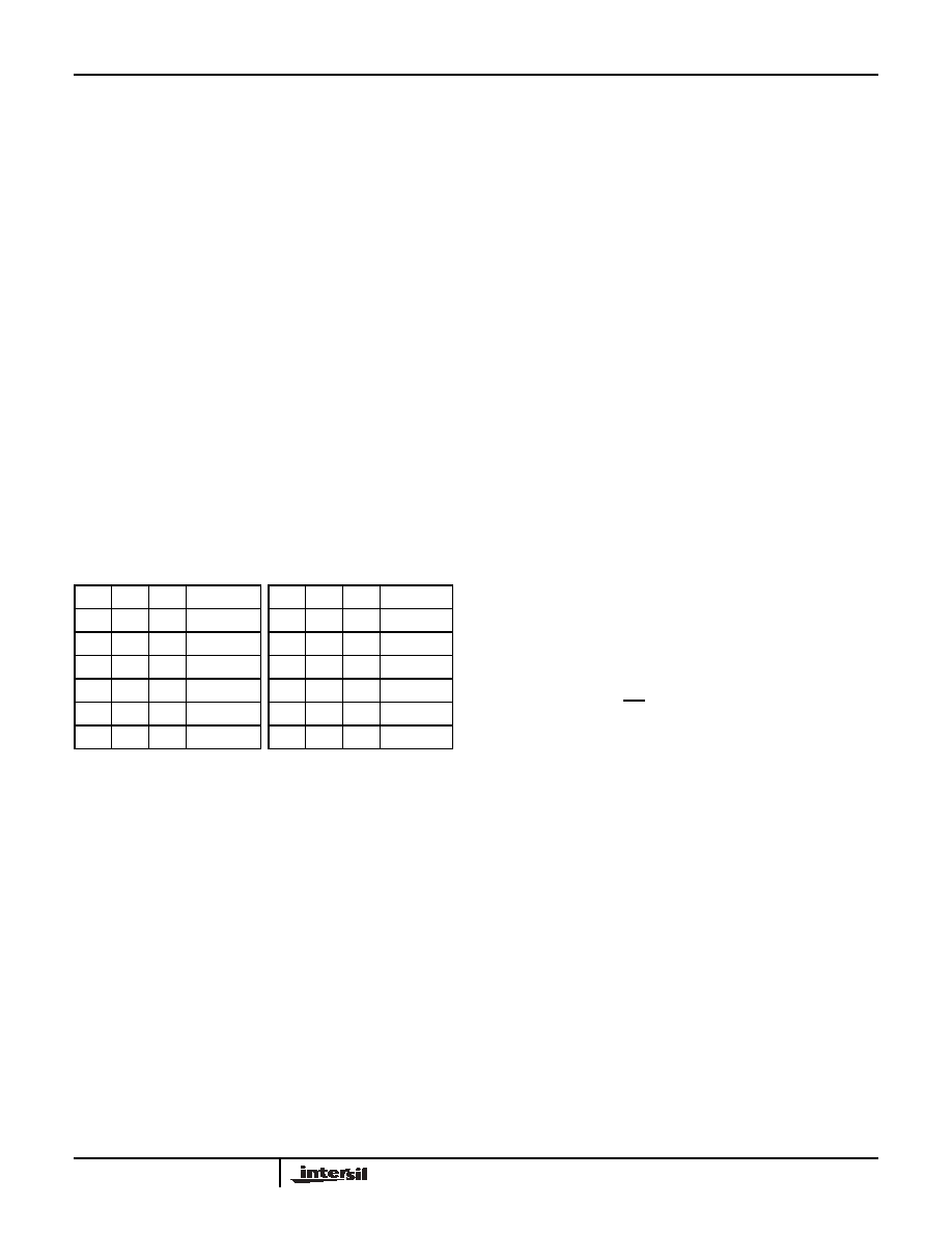
ORDERING INFORMATION
Notes: Y = Yes, N = No
*All options are for 12-bit resolution, industrial temperature operating range, and a 20-pin TSSOP package.
Device
Features
Voltage References
Voltage
Outputs
DAC Control
System
Control
Volt
age R
e
f
O
u
tp
ut
Pin (Vref
)
Fu
ll Scale Vo
ltage
In
pu
t/O
u
t
p
u
t
(VH
)
Zero
Scale Volt
age
In
pu
t/O
u
t
p
u
t
(VL
)
Bu
ffered
O
u
t
(Vb
u
f)
and
Buf
f
er
Fee
dba
ck (VFB
)
w
i
th En
able (O
E)
Inc
r
em
ent
/
Decrem
ent
(U
P,D
O
W
N
)
Slave
Ad
dress Pin
s
Power Read
y (RD
Y
)
X79000V20I
Y
Y
Y
Y
Y
A0, A1, A2
Y
X79001V20I
N
Y
Y
Y
N
A0, A1, A2, A3, A4, A5
Y
X79002V20I
Y
Y
Y
N
Y
A0, A1, A2, A3, A4
Y
SO
RDY
UP
DOWN
OE
Vref
V
SS
Vout
Vbuf
VFB
CLR
CS
SCK
A0
A1
V
CC
A3
VH
VL
A4
A2
SI
SO
RDY
OE
A5
V
SS
Vout
Vbuf
VFB
1
2
3
4
5
6
7
8
9
10
20
19
18
17
16
15
14
13
12
11
1
2
3
4
5
6
7
8
9
10
20
19
18
17
16
15
14
13
12
11
CS
SCK
A0
A1
A2
CLR
V
CC
A3
VH
VL
SI
SO
RDY
UP
DOWN
Vref
A4
V
SS
Vout
DNC
1
2
3
4
5
6
7
8
9
10
20
19
18
17
16
15
14
13
12
11
TSSOP
TSSOP
TSSOP
DNC = Do Not Connect
X79000, X79001, X79002
3
FN8147.0
March 17, 2005
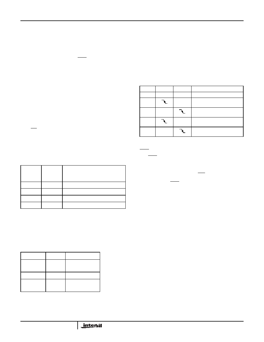
PIN DESCRIPTIONS
Pin Name
Pin Description
CS
SPI Chip Select. CMOS Input Pin. Active low.
SCK
SPI Clock. CMOS Input Pin, with hysteresis.
SI
SPI Serial Data. CMOS Input Pin, with hysteresis.
SO
SPI Serial Data Output Pin. CMOS levels with high impedance state.
RDY
Power-Up "Ready" Indicator Output Pin. Active low. Open drain output.
CLR
Clear DAC Volatile Register Input Pin. Active high. CMOS Input Pin with hysteresis. On-chip pulldown.
A5, A4, A3,
A2, A1, A0
SPI Address Input pins. CMOS Input Pins. On-chip pulldowns.
OE
Buffer Output Enable Input Pin. Active high. CMOS Input Pin with hysteresis. On-chip pulldown.
UP
UP Input pin of the UP/DOWN interface. CMOS Input Pin with deglitching filter. On-chip pulldown.
DOWN
DOWN Input pin of the UP/DOWN interface. CMOS Input Pin with deglitching filter. On-chip pulldown.
V
CC
Power Supply Pin.
V
SS
Ground Pin.
Vout
Unbuffered DAC Output Pin.
Vbuf
Buffered DAC Output Pin.
VFB
Feedback Pin for Buffer Stage.
Vref
Bandgap Voltage Output Pin.
VH
Full Scale Voltage Input or Output Pin.
VL
Zero Scale Voltage Input or Output Pin.
DNC
Do Not Connect
X79000, X79001, X79002

4
FN8147.0
March 17, 2005
ABSOLUTE MAXIMUM RATINGS
All voltages are referred to Vss
Temperature under bias ........................ -40∞C to 85∞C
Storage temperature ......................... -65∞C to +150∞C
Voltage on every pin except Vcc ............. -0.5V to +7V
Voltage on Vcc Pin .....................................-0.5V to 6V
D.C. Output Current at pins SO and RDY............ 5 mA
D.C. Output Current at pins VL, VH,
VFB, Vout and Vref ............................. -0.50 to 1 mA
VBUF output short circuit duration............. 10 seconds
Lead temperature (soldering, 10 seconds)........ 300∞C
COMMENT
Stresses above those listed under "Absolute Maximum
Ratings" may cause permanent damage to the device.
This is a stress rating only; functional operation of the
device (at these or an other conditions above those
listed in the operational sections of this specification) is
not implied. Exposure to absolute maximum rating
conditions for extended periods may affect device
reliability.
RECOMMENDED OPERATING CONDITIONS
ELECTRICAL CHARACTERISTICS
(Unless otherwise specified, all typical values are for 25∞C ambient temperature and 5V at pin Vcc. Maximum and minimum
specifications are over the recommended operating conditions. All voltages are referred to the voltage at pin Vss. All bits in
control registers are "0". SPI interface in "standby" (see notes 1 and 2 on page 6). Output pins unloaded. Input pins floating.
DAC input is 000hex.)
Parameter
Min.
Max.
Units
Temperature
-40
+85
∞C
Voltage on Vcc Pin
4.5
5.5
V
Voltage on any other Pin
-0.3
Vcc +0.3
V
Parameter
Min
Typ
Max
Units
Notes
Buffered DAC and Reference
Resolution
12
bit
INL
±10
LSB
(1)(2)(3)
VL = 0.151V, VH = 3.025V
DNL
-0.5
0.5
LSB
Total Offset Error
12
mV
(1)(2)(4)
VL = 0.151V, VH = 3.025V
Total Fullscale Error
22
mV
Total Offset Error Drift
50
ppm/∞C
(1)(2)(4)
VL = 0.151V, VH = 3.025V
Total Fullscale Error Drift
50
ppm/∞C
Settling time to 1 LSB
2
10
µs
Step size
100mV
(2)(5)
6
30
µs
Step size up to full scale
(2)(5)
Buffer Only
Output Buffer Offset
-6
6
mV
150mV < Vout < V
CC
- 150mV
Output Buffer Offset Drift
-20
20
µV/∞C
(5)
DC PSRR
-1.5
+1.5
mV/V
(5)
Vbuf output slew rate
0.2
V/µs
Output Buffer 3dB Bandwidth
300
1000
kHz
150mV < (V(VFB) =
V(Vbuf)) < V
CC
≠ 150mV
(5)
Digital feed through
10
nV∑sec
(6)
Output load regulation
-1
1
mV/mA
140mV
V(Vbuf)
V
CC
-140mV
I(Vbuf) = ±1mA
Short circuit current @ Vbuf
50
mA
V(Vbuf) = V
CC
or 0V
Capacitive Loading Stability
100
pF
Rload
2k
(5)
X79000, X79001, X79002
5
FN8147.0
March 17, 2005
ELECTRICAL CHARACTERISTICS (continued)
Symbol
Parameter
Min
Typ
Max
Unit
Test Conditions / Notes
Reference
Vrefout
Output Voltage at VRef at 25∞C
1.20
1.21
1.22
V
-20µA < I(VRef) < 0,
Vref as an output
TCOref
Temperature coefficient of VRef
output voltage
50
ppm/
∞C
(5)
R
VHVL
Resistance between VL and VH
9
11.4
14
k
VH & VL external
Digital Interface
t
OEVALID
OE rising edge to output valid
delay
100
µs
t
OEDIS
OE falling edge to high impedance
output delay
100
µs
C
out
SO and RDY pin capacitance
10
pF
Voltage at pin of 0V or Vcc. 1 MHz
signal.
(4)
C
in
CLR, CS, SCK, A0, A1, A2, A3, A4,
A5, SI, UP, DOWN, OE
pin capacitance
8
pF
I
PLDN
On-chip pull down current at A0,
A1, A2, A3, A4, A5, UP, DOWN,
and CLR
0
1
20
µA
Voltage at the pin between 0V and
Vcc
V
ILSPI
CS, SCK and SI input Low voltage
-0.8
0.2 x
Vcc
V
V
IHSPI
CS, SCK and SI input High voltage
0.8 x
Vcc
Vcc +
0.3
V
I
INSPI
CS, CLK and SI input current
-1
10
µA
Voltage at the pin between 0V and
Vcc
V
OHSO
SO output High voltage
Vcc-
0.4
Vcc
V
I(SO) = -2mA
V
OLSO
SO Output Low Voltage
0
0.4
V
I(SO) = 2mA
I
OZSO
SO output High impedance current
-20
+20
µA
V(SO) between 0 and Vcc
V
OLSO
RDY and SO output Low voltage
0
0.4
V
I(SO) or I(RDY) = 2 mA
I
OHRDY
RDY output High current
0
100
µA
V(RDY) = Vcc
V
ILCMOS
CLR, OE, UP, DOWN, A0, A1, A2,
A3, A4, and A5 input Low voltage
-0.3
0.2 x
Vcc
V
V
IHCMOS
CLR, OE, UP, DOWN, A0, A1, and
A2 input High voltage
0.8 x
Vcc
Vcc +
0.3
V
V
HYST
CS, SI, SCK, CLR, OE, UP and
DOWN input hysteresis
0.5
V
(5)
Power Requirements
Iccstby
Standby current into Vcc pin
2.5
mA
V(SCK) = V(SI) = 0 V, V(CS) = Vcc
Iccfull
Full operation current into Vcc pin
3
mA
2-wire interface reading from
memory, 2.5 MHz clock at SCK,
V(OE) = V
CC
, VFB = VBUF
(2)
Iccwrite
Nonvolatile Write current into Vcc
pin
3
mA
Average during internal
non-volatile write cycle
X79000, X79001, X79002
6
FN8147.0
March 17, 2005
Notes: 1. INL, DNL, Offset Error and Full Scale error measured at Vbuf with VFB connected to Vbuf.
2. The V
L
and V
H
levels are set using the configuration register according to the following table:
This setting corresponds to the nominal values of V
H
= 3.025V and V
L
= 0.151V
3. INL is measured at the maximum range of (V
H
-V
L
). INL varies inversely with the range of (V
H
-V
L
). DNL increases at lower
(V
H
-V
L
) ranges but the DAC retains montonicity.
4. Total offset error scales with V
L
according to (1% x V
L
) + 10mV and total full scale error scales with V
H
according to (1% x V
H
) + 10mV
5. Guaranteed by characterization, not 100% tested.
6. f
SCK
= 5MHz, using SPI interface test conditions on pg. 8.
ENDURANCE AND DATA RETENTION (V
CC
= 5V ±10%, T
A
= Full Operating Temprature Range)
SYMBOL TABLE
V
POR
Power-on reset threshold voltage
1.5
2.8
V
V
RDY
RDY indicator minimum voltage
2.6
2.8
V
See figure 1.
T
RDY
RDY indicator delay
100
6000
µs
2k
and 100pF between Vcc and
RDY
(4)
Address
VH2
VH1
VH0
VL2
VL1
VL0
Count 8
Count 10
3Ch
1
0
1
0
0
1
X
X
X = don't care
Parameter
Minimum endurance
100,000
Data changes per bit
Data retention
10
Years
Symbol
Parameter
Min
Typ
Max
Unit
Test Conditions / Notes
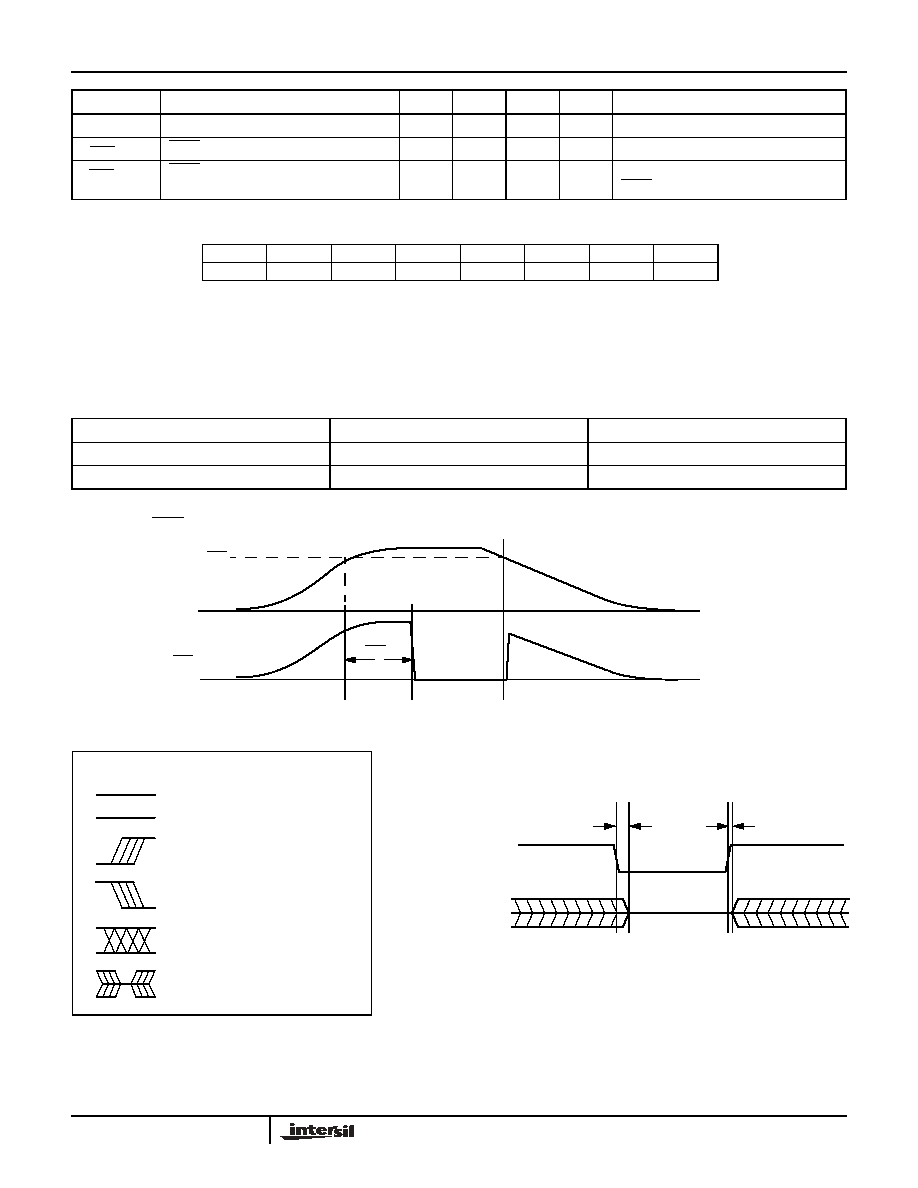
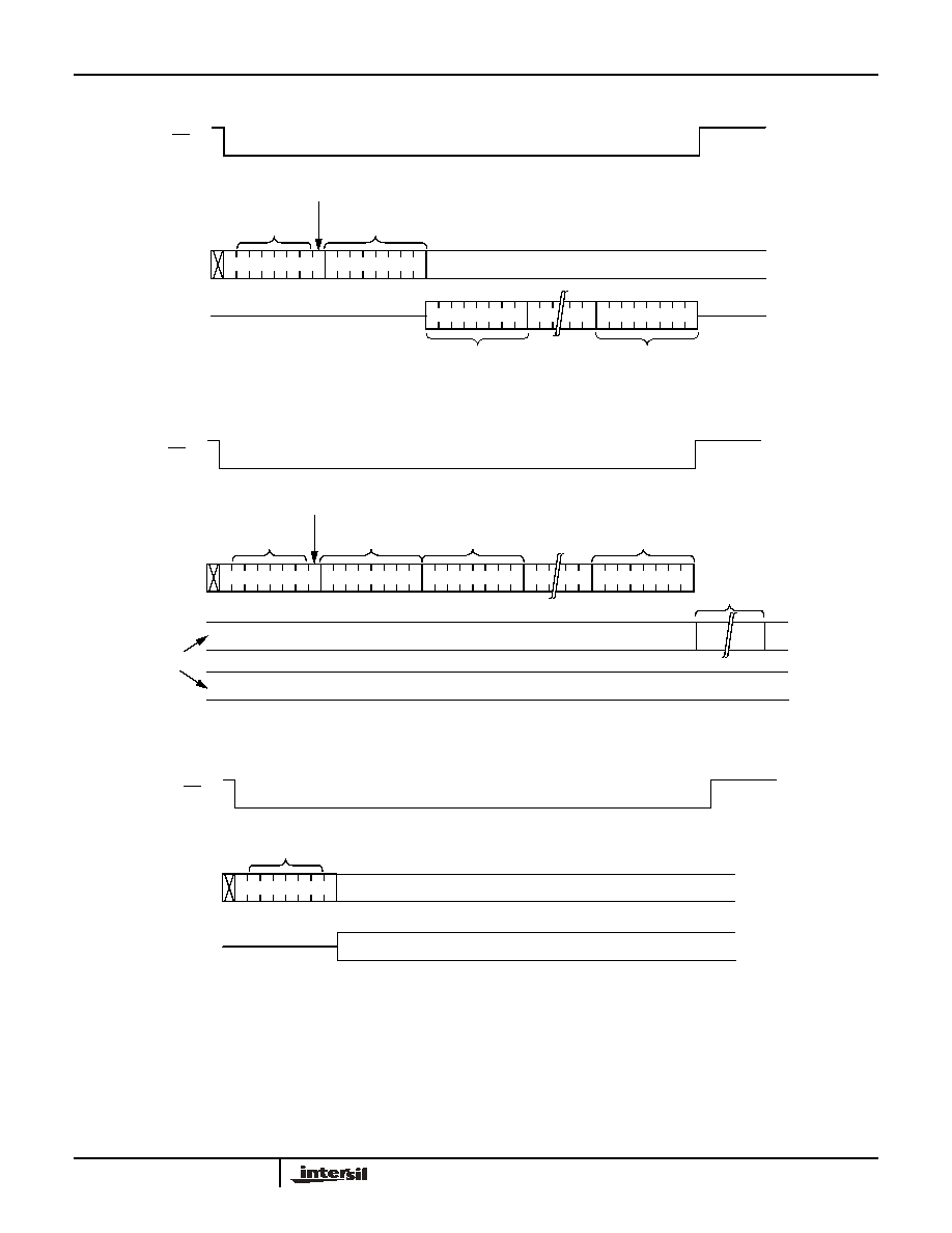
FIGURE 1. RDY PIN TIMING
V
RDY
V
(RDY)
0V
T
RDY
Device
Ready
Power-down
Device Disabled
V
CC
Time
Time
WAVEFORM
INPUTS
OUTPUTS
Must be
steady
Will be
steady
May change
from Low to
High
Will change
from Low to
High
May change
from High to
Low
Will change
from High to
Low
Don't Care:
Changes
Allowed
Changing:
State Not
Known
N/A
Center Line
is High
Impedance
V
OUT
OE
t
OEDIS
t
OEVALID
V
buf = High Impedance
Vbuf OUTPUT ENABLE TIMING
X79000, X79001, X79002
7
FN8147.0
March 17, 2005
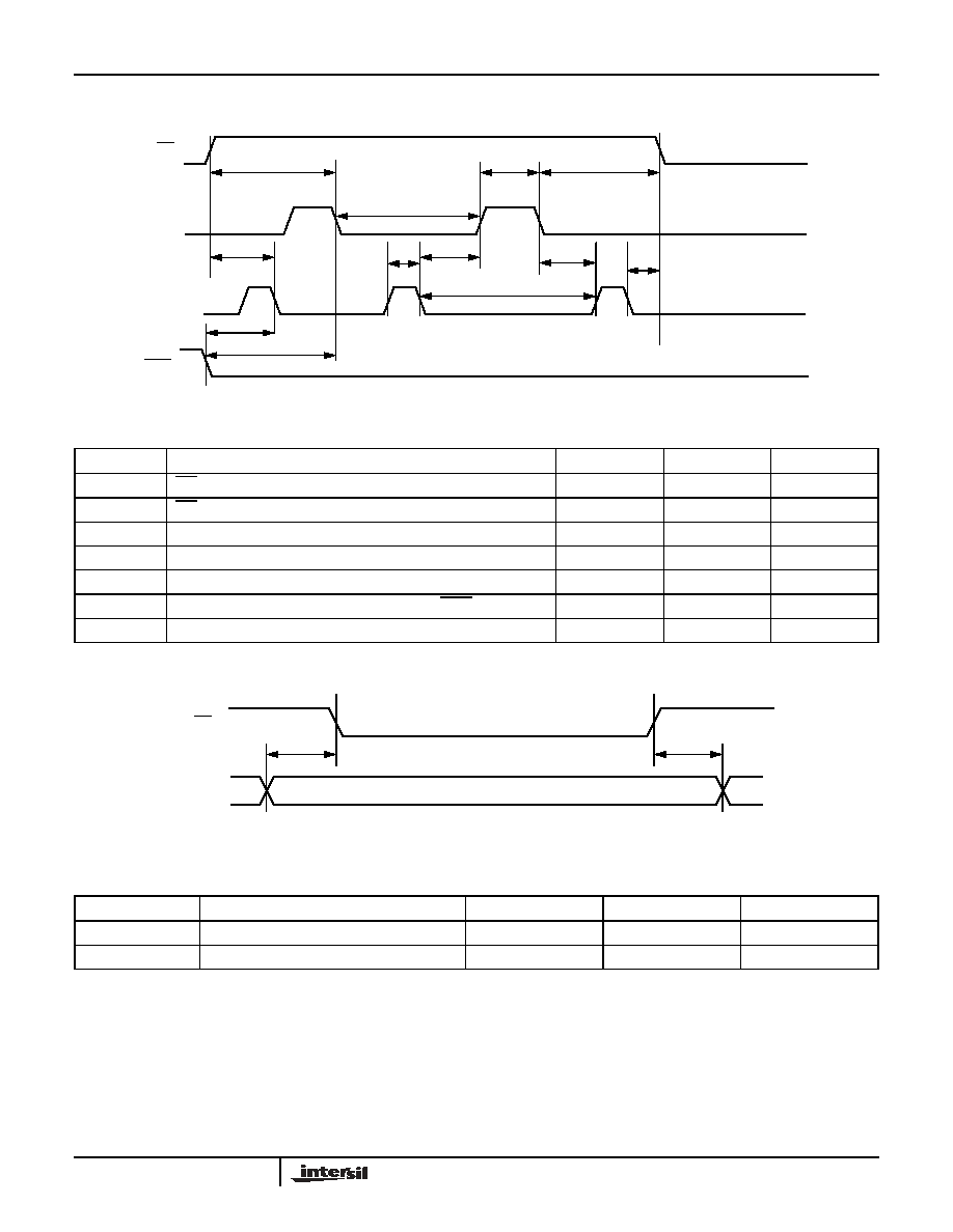
UP/DOWN INTERFACE TIMING
DEVICE ADDRESS PINS TIMING
ADDRESS PINS TIMING
CS
UP
DOWN
RDY
t
UDCSSU
t
UDL
t
UDH
t
UDCSHD
t
UDL
t
UDH
t
UDDIST
t
UDDIST
t
UDCSHD
t
UDCSSU
t
UDRDY
t
UDRDY
Symbol
Parameter
Min
Max
Unit
t
UDCSSU
CS setup time with respect to UP or DOWN
1
µs
t
UDCSHD
CS hold time with respect to UP or DOWN
1
µs
t
UDH
UP or DOWN pulsewidth HIGH
1
µs
t
UDL
UP or DOWN pulsewidth LOW
1
µs
t
UDDIST
UP or DOWN Distance
1
µs
t
UDRDY
(1)
UP or DOWN setup time with respect to RDY
1
µs
t
UDRF
(1)
UP or DOWN rise or fall times
1
µs
Symbol
Parameter
Min
Max
Unit
t
ASU
A0, A1, A2, A3, A4, A5 setup time
1
µs
t
AHO
A0, A1, A2, A3, A4, A5 hold time
1
µs
CS
A0≠A5
t
ASU
(Any Instruction)
t
AHO
X79000, X79001, X79002
8
FN8147.0
March 17, 2005
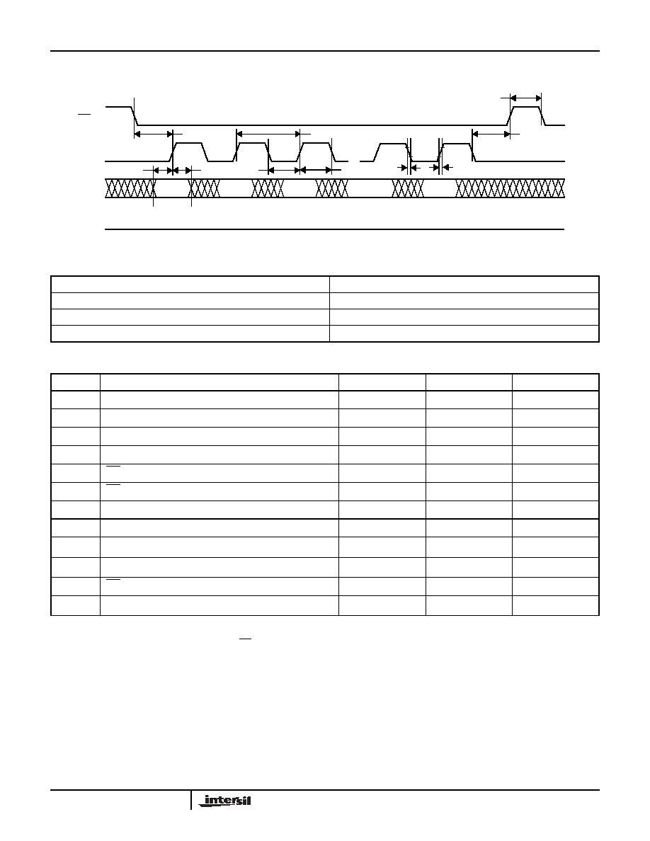
SPI INPUT TIMING
SPI INTERFACE TEST CONDITIONS
SERIAL INPUT TIMING
Notes: 1. These parameters are periodically sampled and not 100% tested.
2. t
WC
is the time from the rising edge of CS after a valid nonvolatile write sequence, to the end of the self-timed internal non-volatile write
cycle. It is the minimum cycle time to be allowed for any non-volatile write cycle by the user, unless the "WIP" bit is used to check for the
end of the write cycle.
Input Pulse Levels
10% to 90% of Vcc
Input Rise and Fall times, between 10% and 90%
10ns
Input and Output Timing Threshold Level
1.4V
External Load at pin SO
2.6k
to Vcc, 3.03k
to Vss, and 10pF to Vss
Symbol
Parameter
Min.
Max.
Unit
f
SCK
Clock Frequency
5
MHz
t
CYC
Cycle Time
200
ns
t
WH
Clock HIGH Time
80
ns
t
WL
Clock LOW Time
80
ns
t
LEAD
CS Lead Time
100
ns
t
LAG
CS Lag Time
100
ns
t
SU
Data Setup Time
20
ns
t
H
Data Hold Time
20
ns
t
RI
(1)
Input Rise Time
20
ns
t
FI
(1)
Input Fall Time
20
ns
t
CS
CS Deselect Time
100
ns
t
WC
(2)
Non-volatile Write Cycle Time
10
ms
...
CS
SCK
SI
SO
MSB
LSB
High Impedance
t
LEAD
t
H
t
SU
t
FI
t
CS
t
LAG
t
CYC
t
WL
...
t
RI
t
WH
X79000, X79001, X79002
9
FN8147.0
March 17, 2005
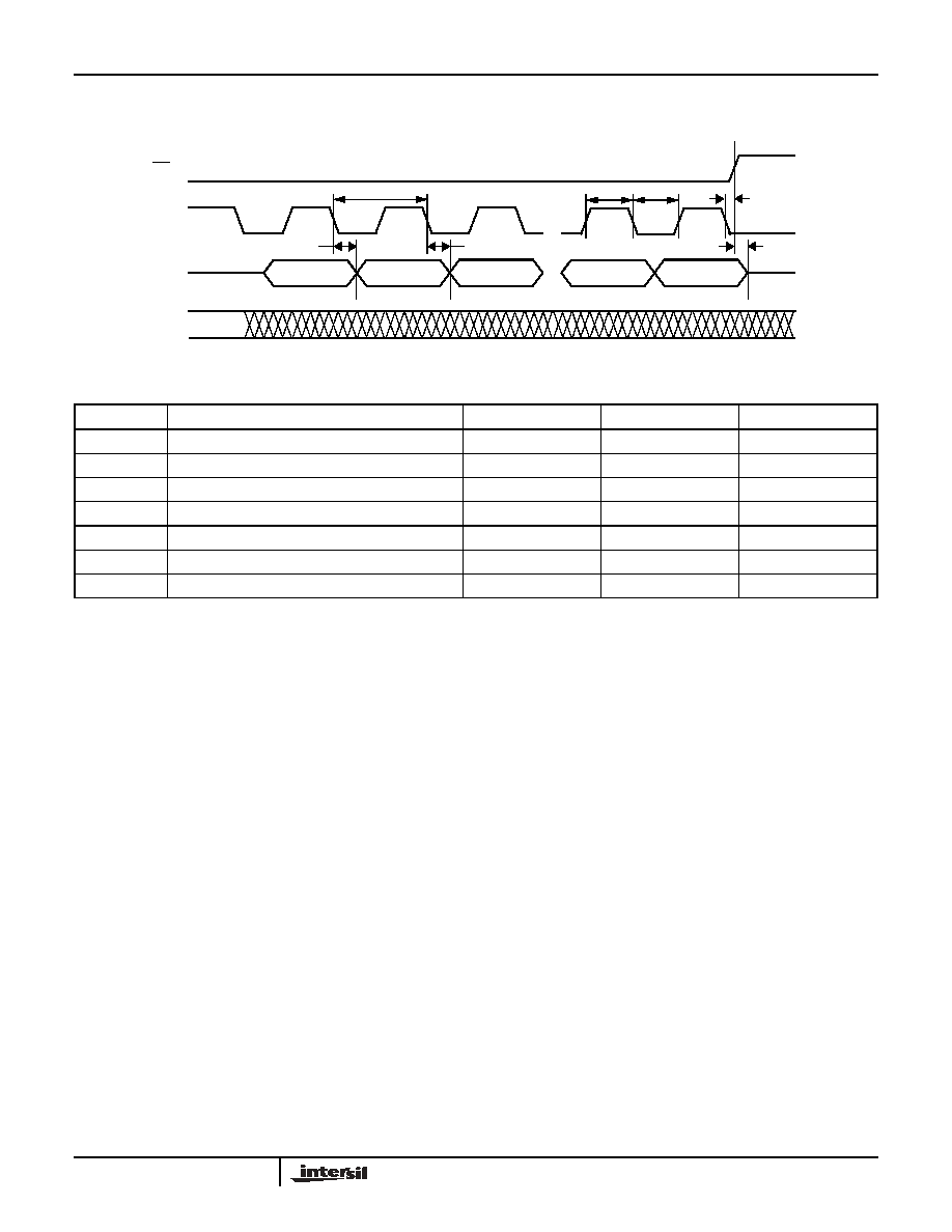
SPI OUTPUT TIMING
SERIAL OUTPUT TIMING
Note:
1. These parameters are periodically sampled and not 100% tested.
Symbol
Parameter
Min.
Max.
Unit
f
SCK
Clock Frequency
5
MHz
t
CYC
Cycle Time
200
ns
t
DIS
(1)
Output Disable Time
50
ns
t
V
(1)
Output Valid from Clock Low
80
ns
t
HO
Output Hold Time
0
ns
t
RO
(1)
Output Rise Time
25
ns
t
FO
(1)
Output Fall Time
25
ns
...
CS
SCK
SO
SI
ADDR
MSB
LSB
t
DIS
t
HO
t
V
...
t
CYC
LSB
t
WH
t
WL
t
LAG
X79000, X79001, X79002
10
FN8147.0
March 17, 2005
DETAILED OPERATION
The X79000 is a versatile 12-bit DAC which allows non-
volatile control over the output range, and consequently
over the resolution of the voltage output.
There are two different ways to adjust the output voltage
of the device. One way is to use the SPI serial bus to
perform a Write command to set the output. This
operation is useful for open loop applications where
simple adjustment of a DC voltage value is desired. The
X79000 offers the unique option of optimizing the
resolution for a given application.
The other way uses the UP/DOWN interface to
increment or decrement the output to converge to a
specific value. This operation is useful for closed loop
systems which can step the output to the desired
position, then disable the interface to hold that value.
Alternatively, the system could continue to increment or
decrement the DAC to update its output control to
compensate for system temperature drifts or other long
term variations.
Output Voltage Span Control
The output voltage span is controlled by 6 MSB's of the
Configuration Register, which is at location 3Ch:
The 3 MSB's control the VH span from 0.605V to 3.025V,
and the next three bits control the VL span from 0.151V
to 2.42V. Note that the selection of a value for VH can
never be lower than that for VL. Regardless of the range
selection, the specified linearity is guaranteed. Thus, if a
particular application requires operation from, say, 1.9V
to 2.4V, then the X79000 can be set for the range of
1.815V to 2.420V, yielding an LSB step size of 148µV. If
a standard DAC were used with a 2.5V reference, then it
would need 14 bits of resolution to get the same LSB
step size.
The VH and VL pins can be used to monitor the selected
reference voltage, or as inputs for external reference
voltages. If an external voltage is to be applied to the VH
or the VL pins, the Configuration Register must be set to
value 000b for that reference to enable the external
reference setting (see Table 1). An externally applied
reference voltage can be time-varying, but the bandwidth
of the device will limit its use as a multiplying DAC to less
than 50kHz or so. The maximum voltage at the VH or VL
pins is 3.1V. Note that although VH and VL can be used
as inputs, the Reference pin (Vref) can only be used as
an output.
The Configuration Register is a non-volatile register, so
when a new VH or VL value is loaded it will be
remembered each time the device is powered up after a
power-down. This function is independent of the status of
the NVDAC bit, which is used only for the DAC registers.
Output Buffer (X79000, X79001 only)
Note that although the voltage span as determined by V
H
is limited to +3.1V max, the output buffer can drive
voltages within 150mV of the positive rail. For a 5V ±5%
V
CC
supply, the DAC can have an output range up to
(4.75 - 0.150V) = 4.60V. The buffer would need a gain >1
set by adding feedback resistors to the V
buf
and V
FB
pins, depending on the V
H
voltage.
For applications requiring voltages greater than 5V,
Intersil recommends the X79002 plus an external buffer.
UP/DOWN Operation
The UP/DOWN functionality of the chip uses the external
pins UP, DOWN, CS and CLR, and also the 2 LSB's of
register 3Ch. The interface is designed to step up or
down by the increments set in register 3Ch. When 12-bit
operation is selected, then the LSB of the device (DAC0)
will increment or decrement with the appropriate pin
action. When 10-bit operation is selected, then third LSB
of the device (DAC2) will change, while leaving the two
LSB's unchanged. When 8-bit operation is selected, then
the fifth LSB of the device (DAC4) will change, an and
the 4 LSB's are unchanged. These options allow the
device to be used as either a 12-bit, 10-bit, or 8-bit DAC
for UP/DOWN applications. The X79000 UP/DOWN
interface allows stepping at up to 500kHz rates.
The CLR pin enables resetting the DAC output register to
all zeroes and can be used to initialize the DAC before
UP/DOWN operation.
VH2 VH1 VH0
Value
VL2 VL1 VL0
Value
0
0
0
external
0
0
0
external
0
0
1
605mV
0
0
1
151mV
0
1
0
1.21V
0
1
0
605mV
0
1
1
1.815V
0
1
1
1.21V
1
0
0
2.42V
1
0
0
1.815V
1
0
1
3.025V
1
0
1
2.42V
X79000, X79001, X79002
11
FN8147.0
March 17, 2005
FUNCTIONAL DESCRIPTION
DAC Register Clear Function
When the input pin CLR is set to logic high, the DAC
volatile register and serial input registers are reset to 000
hex. CLR is an asynchronous input. CLR has an on-chip
pulldown. CLR is ignored while RDY is high.
Buffer Output Enable Function
When the input pin OE is set to logic low, the DAC
buffered output, Vbuf, is set to high impedance.
When the input pin OE is at a logic high, the DAC
buffered output is enabled.
UP/DOWN Interface
The UP/DOWN Interface can be used to change the
value of the DAC register without using the serial
Interface.
The CS pin must be HIGH, when the UP/DOWN
Interface is used, to set the serial interface in standby
mode.
Control bits Count8 and Count10 determine the binary
word that is incremented or decremented, according to
the following table:
These control bits are set by performing a Write
Operation with the serial interface prior to operation of
the UP/DOWN interface.
For example, when Count8 is one, the DAC register
is affected by increment or decrement operations as
follows:
A HIGH to LOW transition on the UP pin, while the
DOWN pin is LOW, increments the selected binary word
by one.
A HIGH to LOW transition on the DOWN pin, while
the UP pin is LOW, decrements the selected binary
word by one.
Other combinations are not valid. See the following table
for a summary of these operations.
X = Don't Care
RDY Pin
The RDY pin is an open drain output which will follow the
V
CC
voltage on power-up (due to the pullups) resistor
and will transition to a low state at time t
RDY
after V
CC
reaches a minimum voltage (V
RDY
). As long as V
CC
is
higher the V
RDY
, the output will remain low. If V
CC
falls
below V
RDY
, the RDY output will return to a high state.
Count8 Count10
Part of DAC register
incremented or
decremented.
0
0
The complete 12 bit word is used
0
1
10 MSBs are used
1
0
8 MSBs are used
1
1
Reserved
8 MSBs
4 LSBs
1000 1011
1000 1010
1110
1110
Increment
Increment
1000 1001
1110
Initial Value
1000 1000
1000 0111
1110
1110
Decrement
Decrement
CS
Up
Down
Mode
L
X
X
SPI Control
H
L
Increment
H
L
Decrement
H
H
Not Allowed
H
H
Not Allowed
X79000, X79001, X79002
12
FN8147.0
March 17, 2005
VOLTAGE REFERENCES
The device includes an on-chip bandgap reference
circuit with 1.21 V nominal output voltage. This voltage is
available at pin VRef as an output.
The voltages at pins VH and VL determine the DAC
output voltage at full scale and zero scale respectively.
Full scale is when the DAC input register is FFF hex (all
ones), and zero scale is when the DAC input register is
000 hex (all zeros).
V(VH) and V(VL) can be generated on-chip and can be
independently programmed to the values indicated in
table 1. VH must always be at a higher voltage than VL.
VH must not be higher than 3.1V. VL & VH can also be
independently disabled, in which case they become
inputs to the device.
SERIAL INTERFACE
Serial Interface Conventions
The device supports the SPI interface hardware protocol.
The protocol defines any device that sends data onto the
bus as a transmitter, and the receiving device as the
receiver. The device controlling the transfer is called the
master and the device being controlled is called the
slave. The master always initiates data transfers, and
provides the clock for both transmit and receive
operations. The X79000 operates as a slave in all
applications.
The device is accessed via the SI and SCK pins, while
the output data is presented at the SO pin. Input data at
pin SI is clocked-in on the rising edge of SCK, when CS
and RDY are both LOW. Output data at pin SO is
clocked-out on the falling edge of SCK.
All commands start with a falling edge at the input pin
CS. Write operations end with a rising edge at the input
pin CS after the last bit of the data bytes being written is
clocked-in. Read operations end with a rising edge at the
input pin CS after the last bit of the data byte being read
is clocked-out.
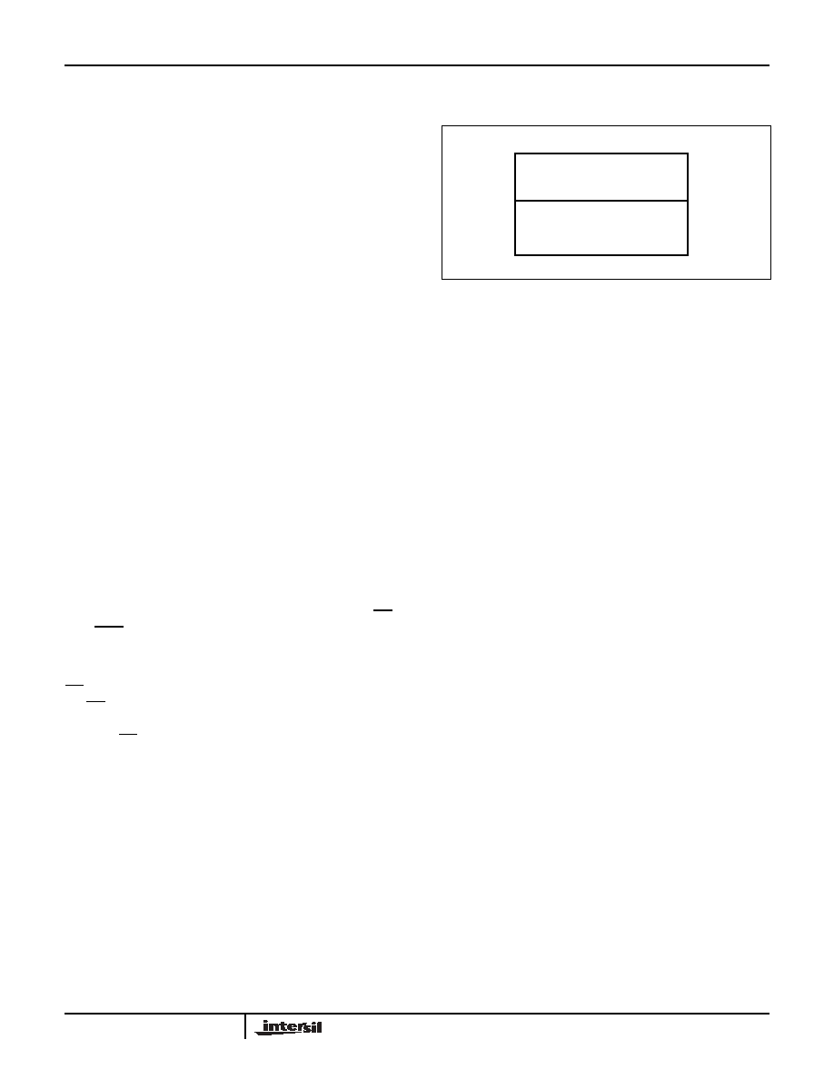
X79000 MEMORY MAP
The X79000 contains a 512-bit array of mixed volatile
and nonvolatile memory. The array is organized as 64
bytes, and it's logically split up into two parts, namely:
≠ General Purpose Memory (GPM)
≠ Control and Status Registers
The GPM is all nonvolatile EEPROM, located at memory
addresses 00h to 37h.
Figure 2. X79000 Memory Map
The Control and Status registers of the X79000 are used
in the test and setup of the device in a system, and
include the DAC volatile register and the DAC nonvolatile
initial value register. These registers are realized as a
combination of both volatile and nonvolatile memory.
These registers reside in the memory locations 38h
through 3Fh. The reserved bits within registers 38h
through 3Dh must be written as "0" if writing to them, and
should be ignored when reading. The reserved registers,
3Ah, 3Bh, 3Eh and 3Fh, must not be written, and their
content should be ignored.
Factory control bit settings:
38h, 39h, 3Fh = All "0"s
3Ch = 1000 0100 (84 hex)
All communication to the X79000 over the SPI bus is
conducted by sending the MSB of each byte of data first.
The memory is physically realized as one contiguous
array, organized as 8 pages of 8 bytes each.
Bit 0
Bit 7
Address
Size
8 Bytes
56 Bytes
00h
37h
38h
3Fh
Control & Status
Registers
General Purpose
Memory (GPM)
...
X79000, X79001, X79002
13
FN8147.0
March 17, 2005
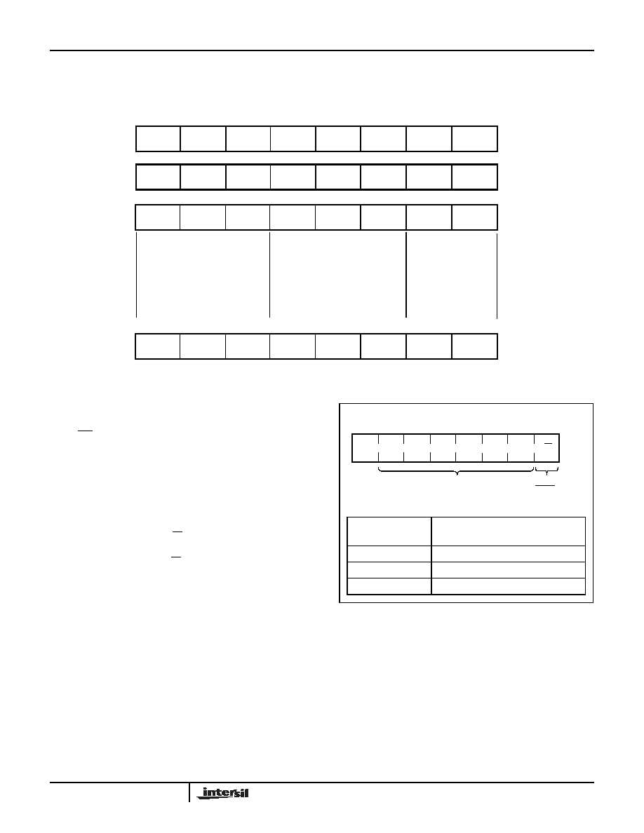
Table 1. Control Registers
IDENTIFICATION AND MEMORY ADDRESS BYTES
The first byte sent to the X79000, following a falling edge
at the CS pin, is called the "Identification Byte". The most
significant bit (ID7) is the function selector bit. The next
six bits (ID6-ID1) are the Device Address bits (AS5-AS0).
To communicate to the X79000, the value of bits AS[5:0]
must correspond to the logic levels at pins A5, A4, A3,
A2, A1, and A0 respectively. If one or more of the
address pins doesn't exist in a particular device, then the
corresponding device address bits must be set to "0".
The LSB (ID0) is the R/W bit. This bit defines the
operation to be performed on the device being
addressed. When the R/W bit is "1", then a Read
operation is selected. A "0" selects a write operation.
If the value of the Device Address bits doesn't match the
logic levels at the Address pins, then the Read or Write
operation is aborted.
The byte sent to the X79000, immediately following the
Identification byte, is called the Memory Address Byte.
The value of this byte is the location of the first byte to
be written to, or read from the X79000. Valid values for
this byte are from 00h to 3Fh. If the value of the
"Memory Address byte" is invalid, the Read or Write
operation is aborted.
Byte
MSB
LSB
38h
Register
MSBs of DAC
DAC5
DAC4
DAC10
DAC9
DAC11
DAC8
DAC7
DAC6
Volatile or
39h
Volatile or
DAC3
DAC2
DAC1
DAC0
Reserved
Reserved Reserved
Reserved
3Ch
Configuration
VH2
VH1
VH0
VL2
VL1
VL0
Count8
Count10
NVDAC
Reserved Reserved Reserved Reserved
Reserved Reserved
Reserved
7
6
5
4
3
2
1
0
Name
Address
Zero Level Configuration
000: External VL reference
001: 151mV
010: 605mV
011: 1.21V
Counter Configuration
00: 12 bits
01: 10 bits
10: 8 bits
11: Reserved
Register
LSBs of DAC
Register
Register
3Fh
Volatile
Non-volatile
Non-volatile
Non-Volatile
Full Scale Configuration
000: External VH reference
001: 605mV
010: 1.21V
011: 1.815V
100: 2.42V
101: 3.025V
100: 1.815V
101: 2.42V
Bytes at addresses 3Ah, 3Bh, 3Dh, and 3Eh are reserved.
110, 111: Reserved
110, 111: Reserved
(for Up/Down Operation)
Non-Volatile
Write Enable
ID6
ID7
ID5
ID3
ID2
ID1
ID0
Read or
ID4
Slave Address
Bit(s)
Description
ID7
Function Selector bit
ID6-ID1
Device Address
ID0
Read or Write Operation Select
R/W
1
AS5
AS4 AS3
Address
Device
AS0
AS1
AS2
Write
X79000, X79001, X79002

14
FN8147.0
March 17, 2005
READ OPERATION
A Read Operation is selected when the R/W bit in the
Identification Byte is set to "1". During a Read Operation,
the X79000 transmits Data Bytes at pin SO, starting at
the first falling edge of SCK, following the rising edge of
SCK that samples the LSB of the Memory Address Byte.
The transmission continues until the CS pin signal goes
HIGH. The Data Bytes are from the memory location
indicated by an internal pointer. This pointer initial value
is the value of the Memory Address Byte, and increments
by one during transmission of each Data Byte. After
reaching memory location 3Fh, the pointer "rolls over" to
00h, and then it continues incremented by one during
each following Data Byte transmission.
If bit "NVDAC" is "1" when reading from byte addresses
38h or 39h, the output is the content of the non-volatile
DAC initial value register. If bit "NVDAC" is "0", the output
is the current value in the volatile DAC register. See the
next section for writing bit "NVDAC".
WRITE OPERATION
A "Write Operation" is selected when the R/W bit in the
Identification Byte is set to "0". The memory array of the
X79000 is organized in 8 pages of 8 bytes each. A single
write operation can be used to write between 1 to 8 bytes
within the same page.
During a Write Operation, the Data Bytes are transmitted
immediately following the Memory Address Byte.
The Data Bytes are written to the memory location
indicated by an internal pointer. This pointer initial value
is the value of the Memory Address Byte, and increments
by one during reception of each Data Byte. After
reaching the highest memory location within a page, the
pointer "rolls over" to the lowest memory location of that
page. The page address remains constant during a
single write operation.
For example, if the Write operation includes 6 Data
Bytes, and the Memory Address byte is 5 (decimal), the
first 3 bytes are written to locations 5, 6, and 7, while the
last 3 bytes are written to locations 0, 1, and 2. If the write
operation includes more than 8 Data Bytes, the new data
overwrites the previous data, one byte at a time.
Bytes at locations 38h through 3Fh are special cases.
Bytes at locations 3Ah, 3Bh, 3Dh, and 3Eh, are reserved
and must not be written. Reserved bits in other bytes
must be set to "0" if writing to those bytes, and should be
ignored when read. The DAC register Bytes at locations
38h & 39h must be written together in a single 2-Byte
write operation.
Location 3Fh contains the "NVDAC" bit. If bit "NVDAC" is
"1", the values of DAC[11:0] are written to non-volatile
memory, otherwise they are written into volatile registers.
Bit "NVDAC" is a volatile bit that has a "0" value at power-
up. The "NVDAC" bit is set to "1" by writing 80h to byte
location 3Fh. It is reset to "0" when the device is powered
down or by writing 00h to byte location 3Fh.
The conifiguration byte at location 3Ch must be written
as a single byte.
NON VOLATILE WRITE:
After a complete write command sequence is correctly
received by the device, and if the write operation is to
non volatile memory, then the X79000 enters an internal
high voltage write cycle that last up to 10 ms.
The internal write cycle starts at the rising edge of CS
that completes the write instruction sequence. The
progress of this internal operation can be monitored
through the "Write In Progress", WIP, bit. The WIP bit
is "1" during the internal write cycle and it's "0"
otherwise. The WIP bit is read with a "Write Status
Polling Command".
X79000, X79001, X79002
15
FN8147.0
March 17, 2005
READ OPERATION
WRITE OPERATION
WRITE STATUS POLLING COMMAND
For every byte, the MSB is transmitted first and the LSB is sent last.
1
0
Last Read
Data Byte
First Read
Data Byte
Read
Memory
Address Byte
CS
Signal
at SI
Signal
at SO
High Impedance
X
Device
Address
0
0
1
0
Device
Address
Write
Memory
Address Byte
CS
Signal
at SI
WIP
bit
When writing to nonvolatile memory.
First Data
Byte to Write
Last Data
Byte to Write
Internal
High Voltage
Write Cycle
0
0
When writing to volatile registers only.
1
1
1
Device
Address
CS
Signal
at SI
High Impedance
Value of "WIP" (Write In Progress) bit
Signal
at SO
X
X79000, X79001, X79002

16
FN8147.0
March 17, 2005
APPLICATIONS INFORMATION
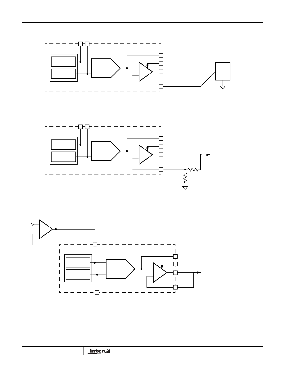
Remote sensing
The output opamp included in the X79000 and X79001 is
normally configured with a gain of +1, and since the
inverting terminal is available externally, can be used for
remote load sensing (see Figure 3). This configuration is
useful for high accuracy applications which may draw
significant current from the DAC output with a finite
impedance from the DAC to the load. The inverting
terminal must be brought as close as possible to the
load, and there must be very low differential in the
ground potentials of the two circuits.
Output Voltages Greater than 3.025V
The opamp output (Vbuf) can drive up to ±1mA and stay
within 150mV of ground and the V
CC
supply. Normally, if
the opamp is configured with a gain of +1, Vbuf is limited
to 3.10V max, which is the limit of the DAC Vout. If gain
is added to the opamp feedback loop, then Vbuf can
provide a higher output voltage, up to 4.85V with
V
CC
= 5.00V. Figure 4 shows a circuit with a gain of +2
that is configured for 4.84V max Vbuf, with VH internally
set to 2.42V (VH2, VH1, VH0 set to 1,0,0). Care must be
taken when increasing the maximum Vbuf output,
however, in this example V
CC
may have a range of ±5%,
or 4.75V to 5.25V. The maximum Vbuf can be expected
to reach and stay within specifications is 4.75V -
150mV = 4.600V. If the output offset of the DAC is
included (22mV x 2, worst case), then the max output will
be 4.84V + 0.044V = 4.884V. The designer has the
option of either realizing that the DAC may miss the
higher codes, or change the amplifier gain to a value less
than 2 (or 4.60/2.42 = 1.90, for this example) to keep all
codes and reduce the maximum Vbuf output.
Using the VH and VL pins for multiplying functions
When a time-varying waveform is applied at either
reference input pin, the output reflects a scaled version of
that waveform (see Figure 5). This waveform will follow
the DAC output voltage equation when applied to VH:
Vbuf = [(VH - VL)(n/4095)] + VL, n = 0 to 4095
(excluding DAC, Reference scaling and opamp errors)
This shows that the input range for the waveform is
limited to VL on the low side, and by the Vout range
(3.10V) on the high side. The output is scaled by the
DAC setting to allow for gain control. The maximum
output voltage can be increased as shown in Figure 4
using the opamp and Vbuf output. It is advisable that the
VH pin be driven by a low impedance source for optimal
AC performance. The minimum bandwidth of the circuit
is 50kHz over all specified voltage range, temperature
and output loading configurations.
Note that it is possible to use the VL pin in the same
fashion, with VH fixed, but the resulting waveform will
have a slightly different transfer function:
Vbuf = VH - (VH
- VL)[(4095-n)/4095], n = 0 to 4095
Alternatively, the VL input could include a variable
reference, such as a temperature sensor, or a shunt
reference connected between VH and VL, which would
fix their differential (the configuration register must be
set for external VH and VL references). This provides a
DAC output which varies proportional to temperature,
yet can be set to an arbitrary voltage by the DAC for
biasing applications.
X79000, X79001, X79002
17
FN8147.0
March 17, 2005
FIGURE 3. REMOTE SENSING
FIGURE 4. ACHIEVING HIGHER OUTPUT VOLTAGES
FIGURE 5. MULTIPLYING DAC CONFIGURATION
Variable Gain
& Level Shift
Variable Gain
& Level Shift
DAC
Core
+
≠
Vbuf
VFB
VH VL
Bias
and
Control
Circuit
X79000
Variable Gain
& Level Shift
Variable Gain
& Level Shift
DAC
Core
+
≠
Vbuf
VFB
VH VL
X79000
Vout = 1.21V to 4.84V*
10K
10K
*Set Register 3Ch for
V
H
= 2.42V
V
L
= 0.605V
or use a Intersil DCP
Variable Gain
& Level Shift
Variable Gain
& Level Shift
DAC
Core
+
≠
Vbuf
VFB
VH
VL
X79000
Vout =
[(V
IN
- V
L
) n/4095] + V
L
+
≠
n = 0 to 4095
(V
L
set to internal reference)
V
IN
X79000, X79001, X79002

18
All Intersil U.S. products are manufactured, assembled and tested utilizing ISO9000 quality systems.
Intersil Corporation's quality certifications can be viewed at www.intersil.com/design/quality
Intersil products are sold by description only. Intersil Corporation reserves the right to make changes in circuit design, software and/or specifications at any time without
notice. Accordingly, the reader is cautioned to verify that data sheets are current before placing orders. Information furnished by Intersil is believed to be accurate and
reliable. However, no responsibility is assumed by Intersil or its subsidiaries for its use; nor for any infringements of patents or other rights of third parties which may result
from its use. No license is granted by implication or otherwise under any patent or patent rights of Intersil or its subsidiaries.
For information regarding Intersil Corporation and its products, see www.intersil.com
FN8147.0
March 17, 2005
PACKAGING INFORMATION
NOTE: ALL DIMENSIONS IN INCHES (IN PARENTHESES IN MILLIMETERS)
20-LEAD PLASTIC, TSSOP PACKAGE TYPE V
.169 (4.3)
.177 (4.5)
.252 (6.4) BSC
.025 (.65) BSC
.252 (6.4)
.260 (6.6)
.002 (.05)
.006 (.15)
.047 (1.20)
.0075 (.19)
.0118 (.30)
See Detail "A"
.031 (.80)
.041 (1.05)
0
∞
- 8
∞
.010 (.25)
.019 (.50)
.029 (.75)
Gage Plane
Seating Plane
Detail A (20X)
(4.16) (7.72)
(1.78)
(0.42)
(0.65)
ALL MEASUREMENTS ARE TYPICAL
X79000, X79001, X79002