
1
Æ
FN8148.0
CAUTION: These devices are sensitive to electrostatic discharge; follow proper IC Handling Procedures.
1-888-INTERSIL or 321-724-7143
|
Intersil (and design) is a registered trademark of Intersil Americas Inc.
Copyright Intersil Americas Inc. 2005. All Rights Reserved
All other trademarks mentioned are the property of their respective owners.
X80000, X80001
Smart Power PlugTM
Penta-Power
Sequence Controller with Hot Swap
The X80000 contains three major functions: a power
communications controller, a power sequencing controller,
and a hotswap controller.
The power communications controller allows smart power
supply control via the backplane using the SMBus protocol.
The system can check for voltage, current, and
manufacturing ID compliance before board insertion. The
power distribution network can monitor the status of the
negative voltage supply, DC voltage supplies, and hardshort
events by accessing the Fault Detection Register and
General Purpose EEPROM of the device. Each device has a
unique slave address for identification.
The power sequencer controller time sequences up to five
DC-DC modules. The X80000 allows for various hardwired
configurations, either parallel or relay sequencing modes.
The power good, enable and voltage good signals provide
for flexible DC-DC timing configurations. Each voltage
enable signal has a programmable delay. In addition, the
voltage good signals can be monitored remotely via the fault
detection register (thru the SMBus).
The hot swap controller allows a board to be safely inserted
and removed from a live backplane without turning off the
main power supply. The X80000 family of devices offers a
modular, power distribution approach by providing flexibility
to solve the hotswap and power sequencing issues for
insertion, operations, and extraction. Hardshort Detection
and Retry with Delay, Noise filtering, Insertion Overcurrent
Bypass, and Gate Current selection are some of the
programmable features of the device.
During insertion, the gate of an external power MOSFET is
clamped low to suppress contact bounce. The
undervoltage/overvoltage circuits and the power on reset
circuitry suppress the gate turn on until the mechanical
bounce has ended. The X80000 turns on the gate with a
user set slew rate to limit the inrush current and incorporates
an electronic circuit breaker set by a sense resistor. After the
load is successfully charged, the PWRGD signal is asserted;
indicating that the device is ready to power sequence the
DC-DC power bricks.
Features
∑ Integrates Three Major Functions
- Smart Power Plug communications
- Programmable power sequencing
- Programmable Hot Swap controller
∑ Smart Power PlugTM
- Intelligent board insertion allows verification of board
and power supply resources prior to system insertion.
- Fault detection register records the cause of the faults
- Soft extraction
- Soft re-insertion
- Remote gate shutdown/turn on
- Power ID/manufacturing ID memory (2kb of EEPROM)
∑ Programmable Power Sequencing
- Sequence up to 5 DC/DC converters.
- Four independent voltage enable pins
- Four programmable time delay circuits
- Soft Power Sequencing - restart sequence without
power cycling.
∑ Hot Swap Controller
- Programmable overvoltage and undervoltage protection
- Undervoltage lockout for battery/redundant supplies
- Programmable slew rate for external FET gate control
- Electronic circuit breaker - overcurrent detection and
gate shut-off
- Programmable overcurrent limit during Insertion
- Programmable hardshort retry with retry failure flag
- Typically operates from -30V to -80V. Tolerates
transients to -200V (limited by external components)
∑ Available Packages
- 32-lead Quad No-Lead Frame (QFN)
Applications
∑ -48V Hot Swap Power Backplane/Distribution Central
Office, Ethernet for VOIP
∑ Card Insertion Detection
∑ Power Sequencing DC-DC/Power Bricks
∑ IP Phone Applications
∑ Databus Power Interfacing
∑ Custom Industrial Power Backplanes
∑ Distributed Power Systems
Data Sheet
March 18, 2005

2
FN8148.0
March 18, 2005
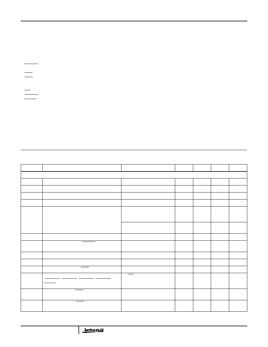
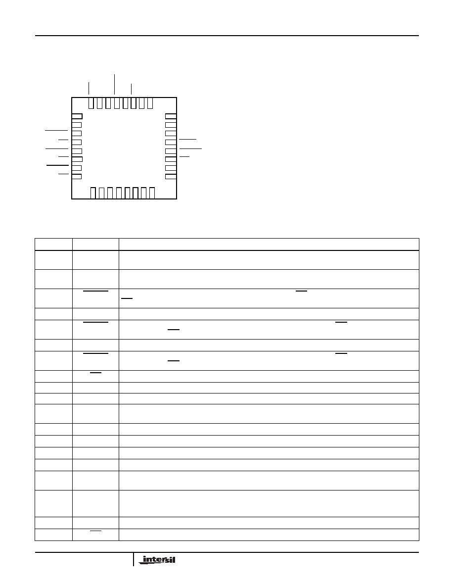
Pinout
X80000, X80001
(7X7 QFN)
TOP VIEW
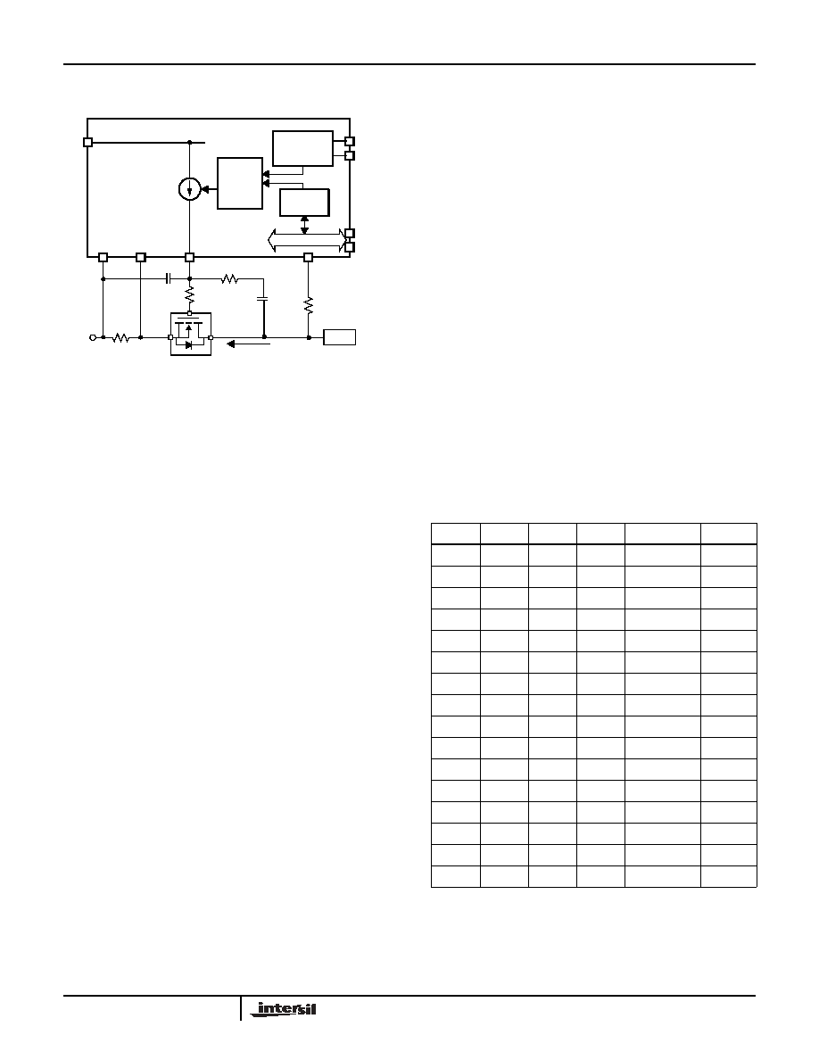
Typical Application
V1GOOD
MRC
A0
V3GOOD
V2GOOD
EN4
EN3
EN1
RESET
WP
V4GOOD
DRAIN
PWRGD
SENS
E
V
UV/O
V
I
GQ
0
V
EE
GA
TE
V
DD
FA
R
BA
T
T
-
O
N
MRH
I
GQ
1
SCL
1
2
3
4
5
6
7
9 10 11 12 13 14
18
19
20
21
22
23
24
26
27
28
29
30
31
32
SDA
EN2
8
17
NC
V
EE
15
25
V
RGO
16
A1
NC
NC
(7mm x 7mm)
Ordering Information
PART
NUMBER
OV
UV1
UV2
TEMP
RANGE
PKG
PART
MARK
X80000Q32I 74.9
42.4
33.2
I
32 Ld
QFN
80000I
X80001Q32I 68.0
42.4
33.2
I
32 Ld
QFN
80001I
V
DD
X80000
V
UV/OV
V
EE
SENSE
DRAIN
-48V
UV=37V
OV=71V
-48V
GATE
Rs
0.02
5%
R4
182K
1%
R5
30K
1%
R6
10K
1%
Q1
IRFR120
RTN
100K
V1GOOD
V2GOOD
V3GOOD
DC-DC
Module
1
ON/OFF
DC-DC
Module
2
ON/OFF
DC-DC
Module
3
ON/OFF
DC-DC
Module
4
ON/OFF
PWRGD
EN1
EN2
EN3
SCL
SCL
4.7V
12V
X80001
V1
V2
V3
V4
100
0.1µF
SDA
Back-
Plane
SDA
MRH
Opto-
Isolation
Insert
Control
4.7K
3.3n
X80000, X80001
3
FN8148.0
March 18, 2005
Absolute Maximum Ratings
Recommended Operating Conditions
Temperature under bias . . . . . . . . . . . . . . . . . . . . . ≠65∞C to +135∞C
Storage temperature . . . . . . . . . . . . . . . . . . . . . . . ≠65∞C to +150∞C
Voltage on given pin (Hot Side Functions):
V
ov/uv pin
. . . . . . . . . . . . . . . . . . . . . . . . . . . . . . . . . . .5.5V + V
EE
SENSE pin . . . . . . . . . . . . . . . . . . . . . . . . . . . . . . . .400mV + V
EE
V
EE
pin. . . . . . . . . . . . . . . . . . . . . . . . . . . . . . . . . . . . . . . . . . -80V
DRAIN pin . . . . . . . . . . . . . . . . . . . . . . . . . . . . . . . . . . 48V + V
EE
PWRGD pin . . . . . . . . . . . . . . . . . . . . . . . . . . . . . . . . . . 7V + V
EE
GATE pin . . . . . . . . . . . . . . . . . . . . . . . . . . . . . . . . . . . V
DD
+ V
EE
FAR pin . . . . . . . . . . . . . . . . . . . . . . . . . . . . . . . . . . . . . 7V + V
EE
MRH pin . . . . . . . . . . . . . . . . . . . . . . . . . . . . . . . . . . . .5.5V + V
EE
BATT_ON pin . . . . . . . . . . . . . . . . . . . . . . . . . . . . . . . .5.5V + V
EE
Voltage on given pin (Cold Side Functions):
ENi pins (i = 1 to 4) . . . . . . . . . . . . . . . . . . . . . . . . . . . . . . . . . .5V
ViGOOD pins (i = 1 to 4) . . . . . . . . . . . . . . . . . . . . . . .5.5V + V
EE
RESET pin . . . . . . . . . . . . . . . . . . . . . . . . . . . . . . . . . .5.5V + V
EE
SDA, SCL, WP, A0, A1 pins . . . . . . . . . . . . . . . . . . . . .5.5V + V
EE
MRC pin . . . . . . . . . . . . . . . . . . . . . . . . . . . . . . . . . . . .5.5V + V
EE
IGQ1 and IGQ0 pins . . . . . . . . . . . . . . . . . . . . . . . . . .5.5V + V
EE
V
DD
pin . . . . . . . . . . . . . . . . . . . . . . . . . . . . . . . . . . . . 14V + V
EE
D.C. output current. . . . . . . . . . . . . . . . . . . . . . . . . . . . . . . . . . . 5mA
Lead temperature (soldering, 10 seconds) . . . . . . . . . . . . . . . 300∞C
Temperature Range (Industrial) . . . . . . . . . . . . . . . . . . -40∞C to 85∞C
Supply Voltage (V
DD
) . . . . . . . . . . . . . . . . . . . . . . . . . . . . . . . . .12V
CAUTION: Stresses above those listed under "Absolute Maximum Ratings" may cause permanent damage to the device. This is a stress rating only; functional
operation of the device (at these or any other conditions above those listed in the operational sections of this specification) is not implied. Exposure to absolute maximum
rating conditions for extended periods may affect device reliability.
Electrical Specifications
Standard Settings
Over the recommended operating conditions unless otherwise specified.
SYMBOL
PARAMETER
TEST CONDITIONS
MIN
TYP
MAX
UNIT
DC CHARACTERISTICS
V
DD
Supply Operating Range
10
12
14
V
I
DD
Supply Current
2.5
5
mA
V
RGO
Regulated 5V output
I
RGO
= 10µA
4.5
5.5
I
RGO
V
RGO
current output
50
µA
I
GATE
Gate Pin Current
Gate Drive On,
V
GATE
= V
EE
,
V
SENSE
= V
EE
(sourcing)
46.2
52.5
58.8
µA
V
GATE
- V
EE
= 3V
V
SENSE
-V
EE
= 0.1V (sinking)
9
mA
V
GATE
External Gate Drive (Slew Rate Control)
I
GATE
= 50µA
V
DD
-0.01
V
DD
V
V
PGA
Power Good Threshold (PWRGD High to Low)
Referenced to V
EE
V
UV1
< V
UV/OV
< V
OV
0.9
1
1.1
V
V
IHB
Voltage Input High (BATT_ON)
V
EE
+ 4
V
EE
+ 5
V
V
ILB
Voltage Input Low (BATT_ON)
V
EE
+ 2
V
I
LI
Input Leakage Current (MRH, MRC)
V
IL
= GND to V
CC
10
µA
I
LO
Output Leakage Current
(V1GOOD, V2GOOD, V3GOOD, V4GOOD,
RESET)
All ENi = V
RGO
for i = 1 to 4
10
µA
V
IL
Input LOW Voltage (MRH, MRC, IGQ0, IGQ1)
-0.5 +
V
EE
(V
EE
+ 5)
x 0.3
V
V
IH
Input HIGH Voltage (MRH, MRC, IGQ0, IGQ1)
(V
EE
+ 5)
x 0.7
(V
EE
+ 5)
+ 0.5
V
X80000, X80001
4
FN8148.0
March 18, 2005
V
OL
Output LOW Voltage
(RESET, V1GOOD, V2GOOD, V3GOOD,
V4GOOD, FAR, PWRGD)
I
OL
= 4.0mA
V
EE
+ 0.4
V
C
OUT
(Note 1)
Output Capacitance
(RESET, V1GOOD, V2GOOD, V3GOOD,
V4GOOD, FAR)
V
OUT
= 0V
8
pF
C
IN
(Note 1) Input Capacitance (MRH, MRC)
V
IN
= 0V
6
pF
V
OC
Overcurrent threshold
V
OC
= V
SENSE
- V
EE
45
50
55
mV
V
OCI
Overcurrent threshold (Insertion)
V
OC
= V
SENSE
- V
EE
PWRGD = HIGH
Initial Power Up condition
135
150
165
mV
V
OVR
Overvoltage threshold (rising)
X80000 Referenced to V
EE
3.85
3.90
3.95
V
X80001
3.49
3.54
3.59
V
V
OVF
Overvoltage threshold (falling)
X80000 Referenced to V
EE
3.82
3.87
3.92
V
X80001
3.46
3.51
3.56
V
V
UV1R
Undervoltage 1 threshold (rising)
Referenced to V
EE
BATT-ON = V
EE
2.19
2.24
2.29
V
V
UV1F
Undervoltage 1 threshold (falling)
2.16
2.21
2.26
V
V
UV2R
Undervoltage 2 threshold (rising)
Referenced to V
EE
BATT-ON = V
RGO
1.71
1.76
1.81
V
V
UV2F
Undervoltage 2 threshold (falling)
1.68
1.73
1.78
V
V
DRAINF
Drain sense voltage threshold (falling)
Referenced to V
EE
0.9
1
1.1
V
V
DRAINR
Drain sense voltage threshold (rising)
Referenced to V
EE
1.2
1.3
1.4
V
V
TRIP1
(Note 1)
EN1 Trip Point Voltage
Referenced to V
EE
V
RGO
˜ 2
V
V
TRIP2
(Note 1)
EN2 Trip Point Voltage
Referenced to V
EE
V
V
TRIP3
(Note 1)
EN3 Trip Point Voltage
Referenced to V
EE
V
V
TRIP4
(Note 1)
EN4 Trip Point Voltage
Referenced to V
EE
V
AC CHARACTERISTICS
t
FOC
Sense High to Gate Low
1.5
2.5
3.5
µs
t
FUV
Under Voltage conditions to Gate Low
0.5
1
1.5
µs
t
FOV
Overvoltage Conditions to Gate Low
1.0
1.5
2
µs
t
VFR
Overvoltage/undervoltage failure recovery time to
Gate =1V.
V
DD
does not drop below 3V, No
other failure conditions.
1.2
1.6
2
µs
t
BATT_ON
Delay BATT_ON Valid
100
ns
t
MRC
Minimum time high for reset valid on the MRC pin
5
µs
t
MRH
Minimum time high for reset valid on the MRH pin
5
µs
t
MRCE
Delay from MRC enable to PWRGD HIGH
No Load
1.0
1.6
µs
t
MRCD
Delay from MRC disable to PWRGD LOW
Gate is On, No Load
200
400
ns
t
MRHE
Delay from MRH enable to Gate Pin LOW
I
GATE
= 60µA, No Load
1.0
1.6
2.4
µs
Electrical Specifications
Standard Settings
Over the recommended operating conditions unless otherwise specified. (Continued)
SYMBOL
PARAMETER
TEST CONDITIONS
MIN
TYP
MAX
UNIT
X80000, X80001

5
FN8148.0
March 18, 2005
Equivalent A.C. Output Load Circuit
t
MRHD
Delay from MRH disable to GATE reaching 1V
I
GATE
= 60µA, No Load
1.8
2.6
µs
t
RESET_E
Delay from PWRGD or ViGOOD to RESET valid
LOW
1
µs
t
QC
Delay from IGQ1 and IGQ0 to valid Gate pin
current
1
µs
t
SC_RETRY
Delay between retries
TSC1 = 0; TSC0 = 0
90
100
110
ms
t
NF
Noise Filter for Overcurrent
TF1 = 0; TF0 = 1
4.5
5
5.5
µs
t
DPOR
Device Delay before Gate assertion
45
50
55
ms
t
SPOR
Delay after PWRGD and all ViGOOD signals are
active before RESET assertion
TPOR1 = 0; TPOR0 = 0
90
100
110
ms
t
TO
ViGOOD turn off time
50
ns
t
PDHLPG
(Note 1)
Delay from Drain good to PWRGD LOW
Gate = V
DD
1
µs
t
PDLHPG
(Note 1)
Delay from Drain fail to PWRGD HIGH
Gate = V
DD
1
µs
t
PGHLPG
(Note 1)
Delay from Gate good to PWRGD LOW
Drain = V
EE
1
µs
t
PGLHPG
(Note 1)
Delay from Gate fail to PWRGD HIGH
Drain = V
EE
1
µs
NOTE:
1. This parameter is based on characterization data.
Electrical Specifications
Standard Settings
Over the recommended operating conditions unless otherwise specified. (Continued)
SYMBOL
PARAMETER
TEST CONDITIONS
MIN
TYP
MAX
UNIT
A.C. Test Conditions
Input pulse levels
V
CC
x 0.1 to V
CC
x 0.9
Input rise and fall times
10ns
Input and output timing levels
V
CC
x 0.5
Output load
Standard output load
5V
SDA
30pF
4.6k
RESET
30pF
V1GOOD,
5V
4.6k
30pF
V2GOOD,
V3GOOD,
V4GOOD,
FAR
5V
4.6k
PWRGD
X80000, X80001
6
FN8148.0
March 18, 2005
SENSE
V
UV/OV
V
OV
V
UV
V
DD
V
TH
MRH
GATE
V
OC
V
OCI
t
VFR
t
FOV
t
FUV
t
DPOR
t
VFR
1V
1V
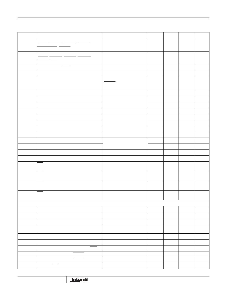
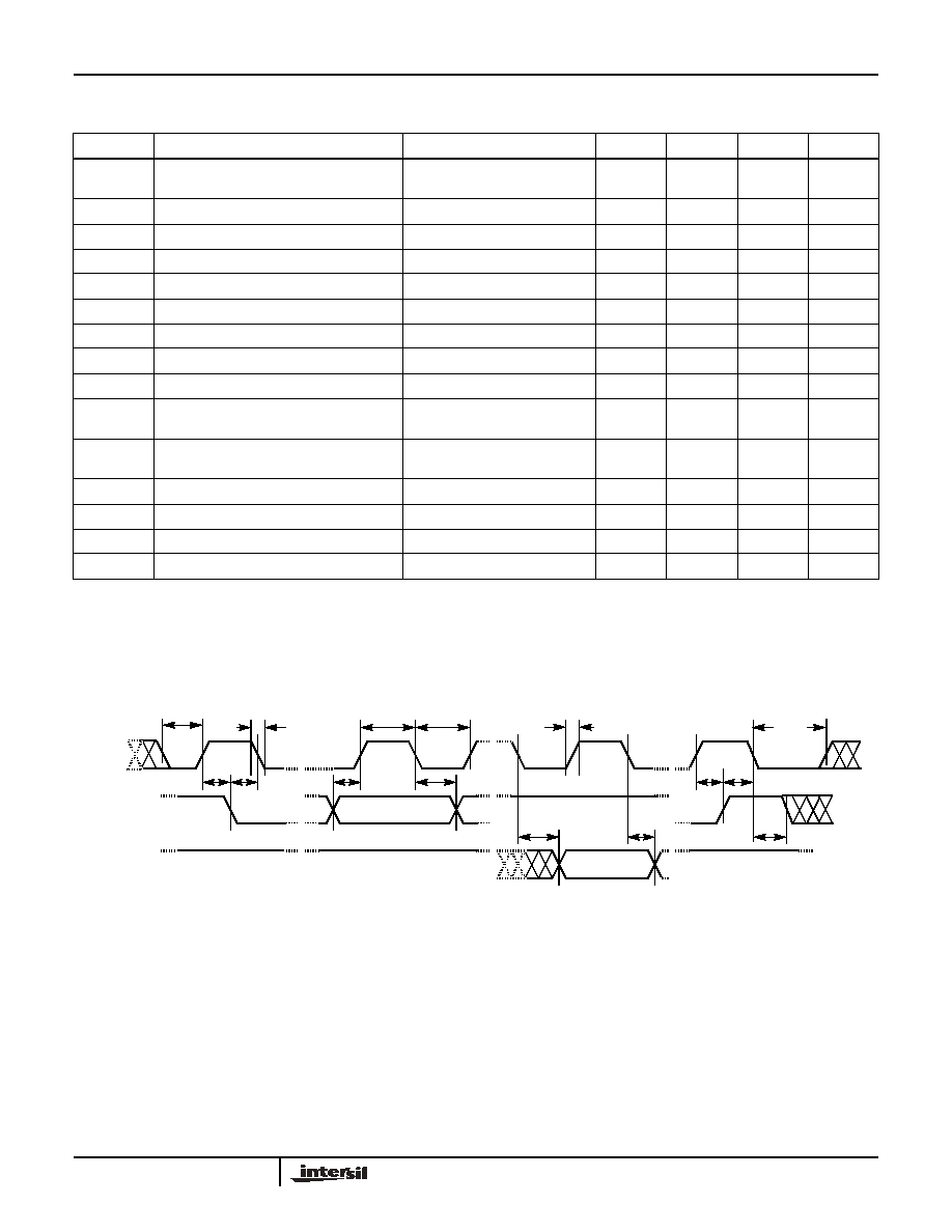
FIGURE 1. OVERVOLTAGE/UNDERVOLTAGE GATE TIMING
SENSE
V
DD
V
TH
GATE
V
OC
V
OCI
t
DPOR
t
SC_RETRY
t
FOC
t
FOC
Always Retry
V
UV
< V
UV/OV
< V
OV
t
SC_RETRY
MRH = HIGH
FIGURE 2. OVERCURRENT GATE TIMING
ENi
t
TO
ViGOOD
V
TRIPi
t
DELAYi
i = 1, 2, 3, 4
Initial
Power-up
t
TO
V
DD
Enable DC/DC supply
FIGURE 3. ViGOOD TIMINGS
X80000, X80001

7
FN8148.0
March 18, 2005
t
MRHD
GATE
t
MRHE
MRH
t
MRH
1V
FIGURE 4. MANUAL RESET (HOT SIDE) MRH
t
MRCD
PWRGD
MRC
t
MRCE
t
MRC
FIGURE 5. MANUAL RESET (COLD SIDE) MRC
PWRGD
t
DELAY1
V1GOOD
t
DELAY2
V2GOOD
t
DELAY3
V3GOOD
t
DELAY4
V4GOOD
t
SPOR
RESET
t
RESET_E
PWRGD or
any ENi LOW to HIGH
V
DRAIN
t
GLHPG
t
GHLPG
(1st occurance)
V
GATE
t
DLHPG
t
DHLPG
ENi
FIGURE 6. PWRGD AND RESET TIMINGS
X80000, X80001

8
FN8148.0
March 18, 2005
Electrical Specifications
Programmable Parameters
Over the recommended operating conditions unless otherwise specified.
SYMBOL
PARAMETER
TEST CONDITIONS
MIN.
TYP.
MAX.
UNIT
DC CHARACTERISTICS
VCB
Over Current Trip Voltage Range
Factory Setting is 50mV (see VOCI).
30
100
mV
I
GATE
(V
CB
= V
SENSE
- V
EE
)
For other options, contact Intersil.
-12
12
%
Gate Pin Pull-Up Current. (error)
(current)
Gate Drive On; V
GATE
= V
EE
, IGQ1=0;
IGQ0=0
IG3 = 0; IG2= 0; IG1 = 0; IG0 = 0 Factory Default
9.2
10.5
11.8
µA
IG3 = 0; IG2= 0; IG1 = 0; IG0 = 1
21.0
µA
IG3 = 0; IG2= 0; IG1 = 1; IG0 = 0
31.5
µA
IG3 = 0; IG2= 0; IG1 = 1; IG0 = 1
42.0
µA
IG3 = 0; IG2= 1; IG1 = 0; IG0 = 0
46.2
52.5
58.5
µA
IG3 = 0; IG2= 1; IG1 = 0; IG0 = 1
63.0
µA
IG3 = 0; IG2= 1; IG1 = 1; IG0 = 0
64.7
73.5
82.3
µA
IG3 = 0; IG2= 1; IG1 = 1; IG0 = 1
84.0
µA
IG3 = 1; IG2= 0; IG1 = 0; IG0 = 0
94.5
µA
IG3 = 1; IG2= 0; IG1 = 0; IG0 = 1
105.0
µA
IG3 = 1; IG2= 0; IG1 = 1; IG0 = 0
115.5
µA
IG3 = 1; IG2= 0; IG1 = 1; IG0 = 1
126.0
µA
IG3 = 1; IG2= 1; IG1 = 0; IG0 = 0
136.5
µA
IG3 = 1; IG2= 1; IG1 = 0; IG0 = 1
147.0
µA
IG3 = 1; IG2= 1; IG1 = 1; IG0 = 0
138.6
157.5
176.4
µA
IG3 = 1; IG2= 1; IG1 = 1; IG0 = 1
168.0
µA
IG3-IG0 = Don't Care IGQ1=0; IGQ0=1
9.2
10.57
11.8
µA
IG3-IG0 = Don't Care IGQ1=1; IGQ0=0
64.7
73.5
82.3
µA
IG3-IG0 = Don't Care IGQ1=1; IGQ0=1
138.6
157.5
176.4
µA
V
PGA
Power Good Threshold Accuracy
V
DRAIN
- V
EE
, High to Low Transition.
Default Factory Setting is 47V.
±400
mV
V
OCI
Over current threshold (Insertion)
Referenced to VEE
VS1 = 0 VS0 = 0
PWRGD = HIGH
45
50
55
mV
VS1 = 0 VS0 = 1
Factory Default
90
100
110
mV
VS1 = 1 VS0 = 0
135
150
165
mV
VS1 = 1 VS0 = 1
180
200
220
mV
AC CHARACTERISTICS
t
SC_RETRY
Delay between Retries
Factory Default
TSC1 = 0 TSC0 = 0
90
100
110
ms
TSC1 = 0 TSC0 = 1
450
500
550
ms
TSC1 = 1 TSC0 = 0
0.9
1
1.1
s
TSC1 = 1 TSC0 = 1
4.5
5
5.5
s
X80000, X80001
9
FN8148.0
March 18, 2005
t
NF
Noise Filter for Overcurrents
Factory Default
F1 = 0 F0 = 0
0
µs
F1 = 0 F0 = 1
4.5
5
5.5
µs
F1 = 1 F0 = 0
9
10
11
µs
F1 = 1 F0 = 1
18
20
22
µs
t
SPOR
Delay before RESET assertion
Factory Default
TPOR1 = 0 TPOR0 = 0
90
100
110
ms
TPOR1 = 0 TPOR0 = 1
450
500
550
ms
TPOR1 = 1 TPOR0 = 0
0.9
1
1.1
s
TPOR1 = 1 TPOR0 = 1
4.5
5
5.5
s
t
DELAYi
Time Delay used in Power
Sequencing (i = 1 to 4)
Factory Default
TiD1 = 0 TiD0 = 0
90
100
110
ms
TiD1 = 0 TiD0 = 1
450
500
550
ms
TiD1 = 1 TiD0 = 0
0.9
1
1.1
s
TiD1 = 1 TiD0 = 1
4.5
5
5.5
s
Serial Interface
Over the recommended operating conditions unless otherwise specified.
SYMBOL
PARAMETER
TEST CONDITIONS
MIN
TYP
MAX
UNIT
DC CHARACTERISTICS
I
CC1
(Note 1)
Active Supply Current (V
DD
) Read to
Memory or CRs
V
IL
= V
CC
x 0.1
V
IH
= V
CC
x 0.9,
f
SCL
= 400kHz
2.5
mA
I
CC2
(Note 1)
Active Supply Current (V
DD
)
Write to Memory or CRs
3.0
mA
I
LI
Input Leakage Current (SCL, WP, A0, A1)
V
IL
= GND to V
CC
10
µA
I
LO
Output Leakage Current (SDA)
V
SDA
= GND to V
CC
Device is in Standby (Note 2)
10
µA
V
IL
(Note 3) Input LOW Voltage (SDA, SCL, WP, A0, A1)
-0.5 + VEE
(V
EE
+ 5) x
0.3
V
V
IH
(Note 3) Input HIGH Voltage (SDA, SCL, WP, A0, A1)
(V
EE
+ 5)
x
0.7
(V
EE
+ 5) +
0.5
V
V
HYS
Schmitt Trigger Input Hysteresis
Fixed input level
V
EE
+ 0.2
V
V
CC
related level
.05 x
(V
EE
+ 5)
V
V
OL
Output LOW Voltage (SDA)
I
OL
= 4.0mA (2.7-5.5V)
I
OL
= 2.0mA (2.4-3.6V)
V
EE
+
0.4
V
AC CHARACTERISTICS
f
SCL
SCL Clock Frequency
400
kHz
t
IN
Pulse width Suppression Time at inputs
50
ns
t
AA
SCL LOW to SDA Data Out Valid
0.1
1.5
µs
Electrical Specifications
Programmable Parameters
Over the recommended operating conditions unless otherwise specified. (Continued)
SYMBOL
PARAMETER
TEST CONDITIONS
MIN.
TYP.
MAX.
UNIT
X80000, X80001
10
FN8148.0
March 18, 2005
Timing Diagrams
t
BUF
Time the bus is free before start of new
transmission
1.3
µs
t
LOW
Clock LOW Time
1.3
µs
t
HIGH
Clock HIGH Time
0.6
µs
t
SU:STA
Start Condition Setup Time
0.6
µs
t
HD:STA
Start Condition Hold Time
0.6
µs
t
SU:DAT
Data In Setup Time
100
ns
t
HD:DAT
Data In Hold Time
0
µs
t
SU:STO
Stop Condition Setup Time
0.6
µs
t
DH
Data Output Hold Time
50
ns
t
R
SDA and SCL Rise Time
20 +.1Cb
(Note 1)
300
ns
t
F
SDA and SCL Fall Time
20 +.1Cb
(Note 1)
300
ns
t
SU:WP
WP Setup Time
0.6
µs
t
HD:WP
WP Hold Time
0
µs
Cb
Capacitive load for each bus line
400
pF
t
WC
(Note 2) EEPROM Write Cycle Time
5
10
ms
NOTE:
2. t
WC
is the time from a valid stop condition at the end of a write sequence to the end of the self-timed internal nonvolatile write cycle. It is the
minimum cycle time to be allowed for any nonvolatile write by the user, unless Acknowledge Polling is used.
Serial Interface
(Continued)
Over the recommended operating conditions unless otherwise specified.
SYMBOL
PARAMETER
TEST CONDITIONS
MIN
TYP
MAX
UNIT
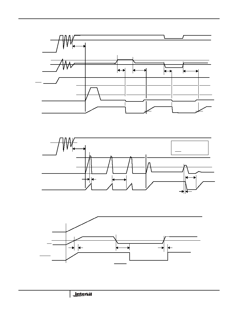
FIGURE 7. BUS TIMING
t
SU:STO
t
HIGH
t
SU:STA
t
HD:STA
t
HD:DAT
t
SU:DAT
SCL
SDA IN
SDA OUT
t
F
t
LOW
t
HD:DAT
t
R
t
DH
t
AA
t
BUF
t
HD:STO
t
BUF
X80000, X80001

11
FN8148.0
March 18, 2005
Symbol Table
t
HD:WP
SCL
SDA IN
WP
t
SU:WP
Clk 1
Clk 9
Slave Address Byte
START
FIGURE 8. WP PIN TIMING
SCL
SDA
8
th
Bit of Last Byte
ACK
Stop
Condition
Start
Condition
FIGURE 9. WRITE CYCLE TIMING
t
WC
Must be
steady
Will be
steady
May change
from LOW
Will change
from LOW
to HIGH
May change
from HIGH
to LOW
Will change
from HIGH
to LOW
Don't Care:
Changes
Allowed
Changing:
State Not
Known
WAVEFORM INPUTS
OUTPUTS
to HIGH
X80000, X80001
12
FN8148.0
March 18, 2005
Typical Performance Characteristics
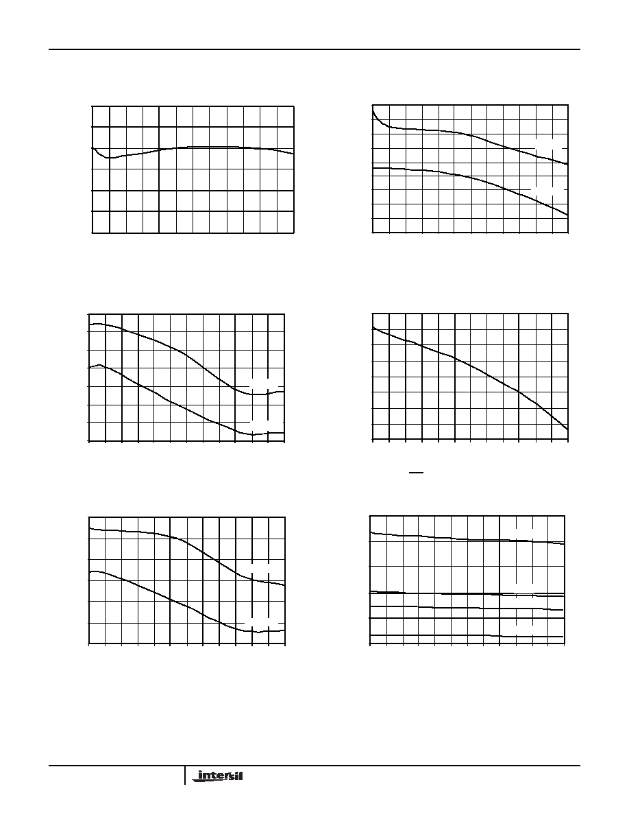
FIGURE 10. OVERCURRENT THRESHOLD vs TEMPERATURE
FIGURE 11. UNDERVOLTAGE 1 THRESHOLD vs
TEMPERATURE
FIGURE 12. OVERVOLTAGE THRESHOLD vs TEMPERATURE
FIGURE 13. ENi THRESHOLD vs TEMPERATURE
FIGURE 14. UNDERVOLTAGE 1 THRESHOLD vs
TEMPERATURE
FIGURE 15. I
GATE
(SOURCE) vs TEMPERATURE
46.000
47.000
48.000
49.000
50.000
51.000
52.000
-55
-40 -25 -10
5
20
35
50
65
80
95
110 12
TEMPERATURE
INR
U
SH CURRENT
LIMIT (m
V
)
1.690
1.700
1.710
1.720
1.730
1.740
1.750
1.760
1.770
1.780
-55
-40 -25 -10
5
20
35
50
65
80
95
110 125
TEMPERATURE
RISING
FALLING
UNDE
R
V
OL
T
A
GE
2
THRES
H
OLD (V
)
3.85
3.86
3.87
3.88
3.89
3.90
3.91
3.92
-55 -40 -25 -10
5
20
35
50
65
80
95 110 125
TEMPERATURE
RISING
FALLING
O
V
THRESHOL
D (V)
2.475
2.480
2.485
2.490
2.495
2.500
2.505
2.510
2.515
-55 -40 -25 -10
5
20
35
50
65
80
95 110 125
TEMPERATURE
E
N
i TH
RE
SHOLD (V)
2.190
2.200
2.210
2.220
2.230
2.240
2.250
-55
-40 -25 -10
5
20
35
50
65
80
95 110 125
TEMPERATURE
RISING
FALLING
UND
E
R
V
O
L
T
A
G
E
1 THRES
H
OLD (
V
)
0
40
80
120
160
200
-55 -40 -25 -10
5
20
35
50
65
80
95 110 125
TEMPERATURE
150µA
70µA
50µA
10µA
GA
TE CU
RRE
NT
(µA)
X80000, X80001
13
FN8148.0
March 18, 2005
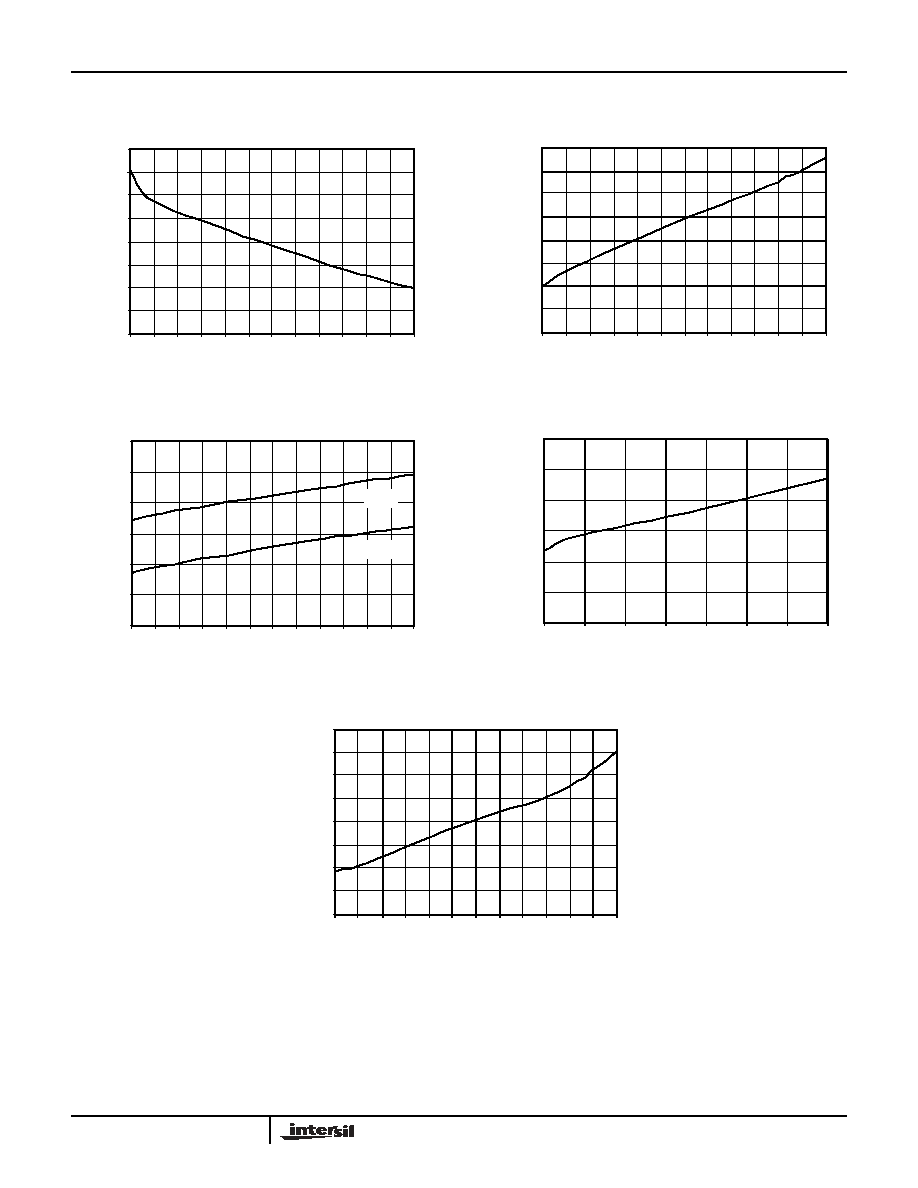
FIGURE 16. I
GATE
(SINK) vs TEMPERATURE
FIGURE 17. t
FOC
vs TEMPERATURE
FIGURE 18. t
FUV
vs TEMPERATURE
FIGURE 19. t
DELAYi
vs TEMPERATURE
FIGURE 20. t
FOV
vs TEMPERATURE
Typical Performance Characteristics
(Continued)
7.0
7.5
8.0
8.5
9.0
9.5
10.0
10.5
11.0
-55 -40 -25 -10
5
20
35
50
65
80
95 110 125
TEMPERATURE
GA
TE CUR
RE
NT
- SINK
(mA)
1.7
1.8
1.9
2.0
2.1
2.2
2.3
2.4
2.5
-55 -40 -25 -10
5
20
35
50
65
80
95 110 125
TEMPERATURE
t
OC
(µs)
0.500
0.550
0.600
0.650
0.700
0.750
0.800
-55
-40 -25 -10
5
20
35
50
65
80
95 110 125
TEMPERATURE
tUV1
tUV2
t
UV
(µ
s)
0.90
0.92
0.94
0.96
0.98
1.00
1.02
-55
-35
-15
5
25
45
65
85
TEMPERATURE
t
DELA
Y
(NORMALIZE
D)
1.0
1.1
1.1
1.2
1.2
1.3
1.3
1.4
1.4
-55 -40
-25 -10
5
20
35
50
65
80
95 110 125
TEMPERATURE
t
OV
(µs)
X80000, X80001
14
FN8148.0
March 18, 2005
SENSE
V
EE
GATE
IGQ1
IGQ0
DRAIN
BATT-ON
MRC
MRH
EN1
EN2
EN3
EN4
V4GOOD
V3GOOD
V2GOOD
V1GOOD
A1
A2
WP
SCL
SDA
RESET
V
DD
FAR
PWRGD
Power Good
Logic
Slew Rate
Selection
EEPROM
2kbits
5V
V
RGO
Bus I
n
ter
f
ac
e
V
EE
V
EE
V
EE
V
EE
V
EE
V
EE
V
OV
Ref
V
UV1
Ref
V
UV2
Ref
V
UV/OV
2:1
MUX
V
EE
Gate
Control
V
DD
1V Ref
V
RGO
Programmable
V
OC
REF
36R
R
R
R
R
Over
current
x1
x2
x3
x4
Reset Logic
and Delay
V
EE
Over current
logic, Hard short
relay, Retry logic
status and delay
POR
Control and
Fault
Registers
10-160µA
Divider
4
Reset
OSC
0.1s
0.5s
1s
5s
Select
4
delay1
delay2
delay3
delay4
Delay circuit
repeated 4 times
V
RGO
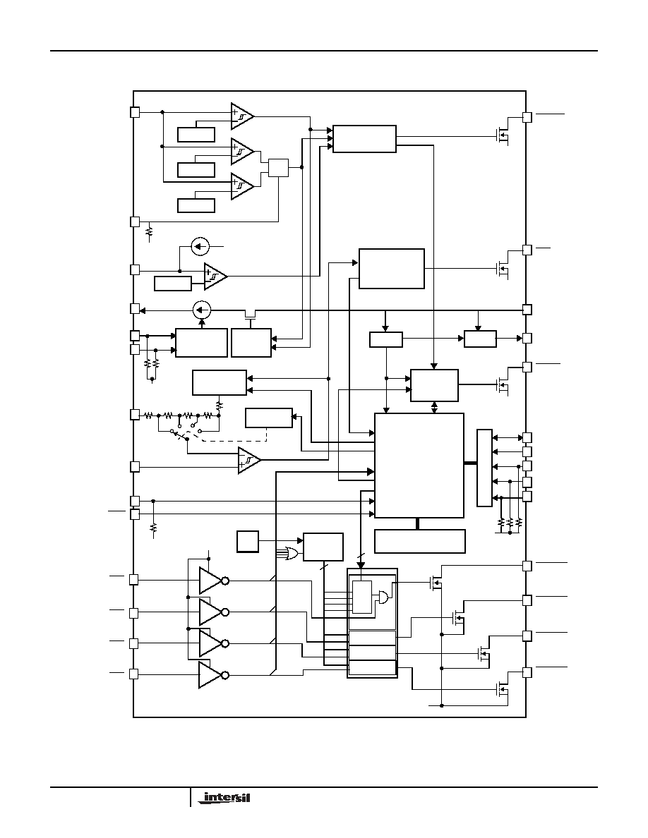
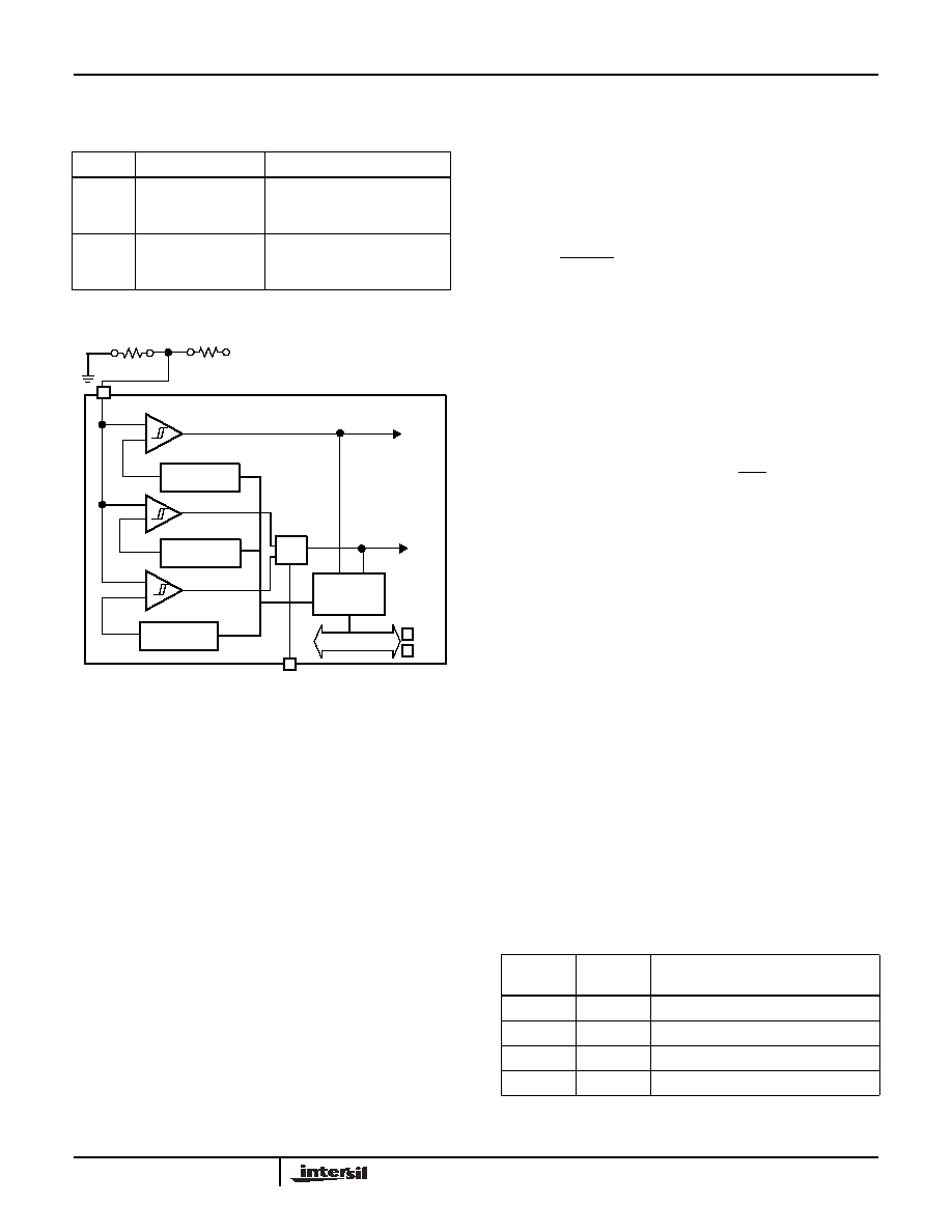
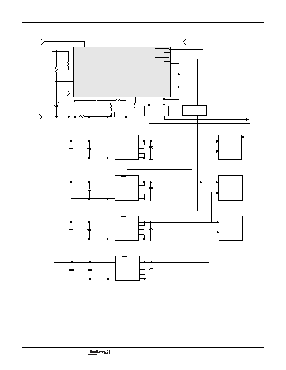
FIGURE 21. BLOCK DIAGRAM
X80000, X80001
15
FN8148.0
March 18, 2005
Pin Configuration
V1GOOD
MRC
A0
V3GOOD
V2GOOD
EN4
EN3
EN1
RESET
WP
V4GOOD
DRAIN
PWRG
D
SE
N
S
E
V
UV/O
V
I
GQ
0
V
EE
GA
TE
V
DD
FA
R
BA
T
T
-
O
N
MRH
I
GQ
1
SCL
1
2
3
4
5
6
7
9 10 11 12 13 14
18
19
20
21
22
23
24
26
27
28
29
30
31
32
X80000/X80001
32-lead QFN Quad Package
SDA
EN2
8
17
NA
V
EE
15
25
V
RGO
16
A1
NC
NC
(7mm x 7mm)
Pin Descriptions
PIN
NAME
DESCRIPTION
1
V
RGO
Regulated 5V output. Used to pull-up user programmable inputs IGQ0, IGQ1, BATT-ON, A1, A0, and WP (if
needed).
2
A0
Address Select Input. It has an internal pulldown resistor. (>10M
typical)
The A0 and A1 bits allow for up to 4 X80000 devices to be used on the same SMBus serial interface.
3
V4GOOD
V4 Voltage Good Output. This open drain output goes LOW when EN4 is less than V
TRIP4
and goes HIGH when
EN4 is greater than V
TRIP4
. There is a user selectable delay circuitry on this pin.
4
EN4
V4 Voltage Enable Input. Fourth voltage enable pin. If unused connect to V
RGO
.
5
V3GOOD
V3 Voltage Good Output (Active Low). This open drain output goes LOW when EN3 is less than V
TRIP3
and
goes HIGH when EN3 is greater than V
TRIP3
. There is a user selectable delay circuitry on this pin.
6
EN3
V3 Voltage Enable Input. Third voltage enable pin. If unused connect to V
RGO
.
7
V2GOOD
V2 Voltage Good Output (Active Low). This open drain output goes LOW when EN2 is less than V
TRIP2
and
goes HIGH when EN2 is greater than V
TRIP2
. There is a user selectable delay circuitry on this pin.
8
EN2
V2 Voltage Enable Input. Second voltage enable pin. If unused connect to V
RGO
.
9
V
DD
Positive Supply Voltage Input.
10
V
EE
Negative Supply Voltage Input.
11
V
UV/OV
Analog Undervoltage and Overvoltage Input. Turns off the external N-channel MOSFET when there is an
undervoltage or overvoltage condition.
12
SENSE
Circuit Breaker Sense Input. This input pin detects the overcurrent condition.
13
GATE
Gate Drive Output. Gate drive output for the external N-channel MOSFET.
14
DRAIN
Drain. Drain sense input of the external N-channel MOSFET.
15
NA
Not Available. Do not connect to this pin.
16
A1
Address Select Input. It has an internal pulldown resistor. (>10M
typical)
The A0 and A1 bits allow for up to 4 X80000 devices to be used on the same SMBus serial interface.
17
SDA
Serial Data. SDA is a bidirectional pin used to transfer data into and out of the device. It has an open drain output
and may be wire ORed with other open drain or open collector outputs. This pin requires a pull up resistor and the
input buffer is always active (not gated).
18
SCL
Serial Clock. The Serial Clock controls the serial bus timing for data input and output.
19
EN1
V1 Voltage Enable Input. First voltage enable pin. If unused connect to V
RGO
.
X80000, X80001
16
FN8148.0
March 18, 2005
Functional Description
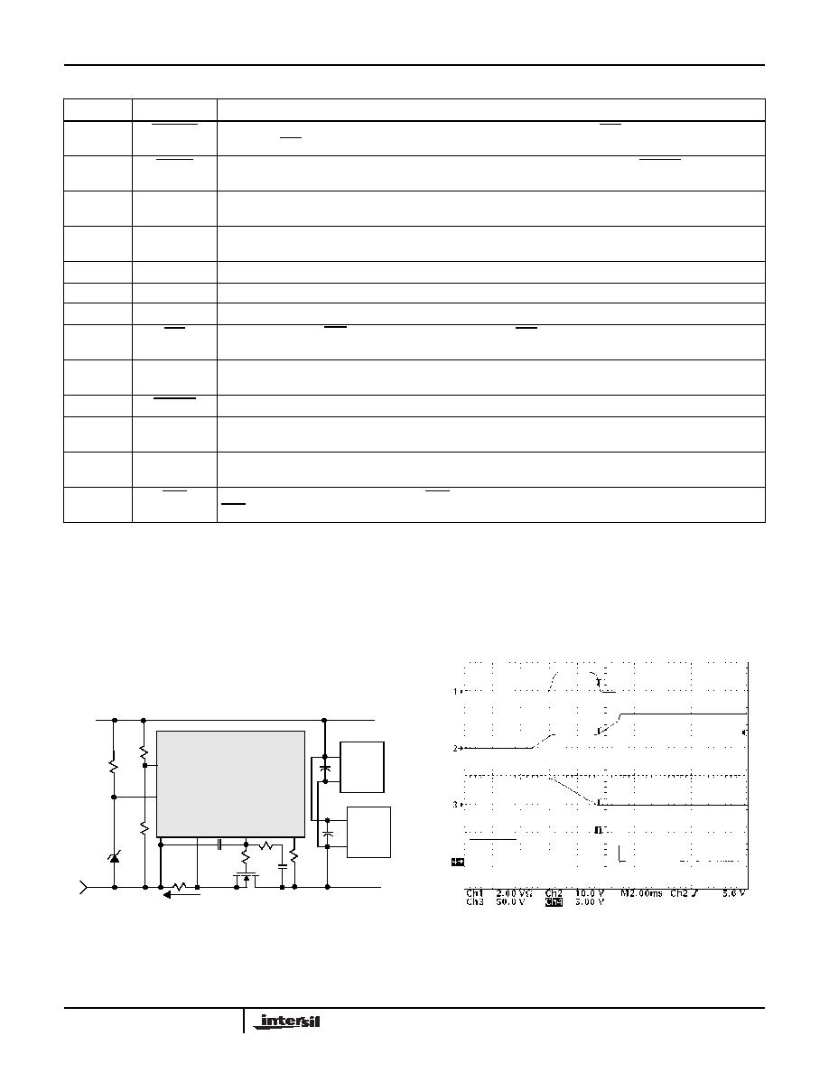
Hot Circuit Insertion
When circuit boards are inserted into a live backplane, the
bypass capacitors at the input of the board's power module
or DC/DC converter can draw huge transient currents as
they charge up (See Figure 22). This transient current can
cause permanent damage to the board's components and
cause transients on the system power supply.
The X80000 is designed to turn on a board's supply voltage
in a controlled manner (see Figure 23), allowing the board to
be safely inserted or removed from a live backplane. The
device also provides undervoltage, overvoltage and
overcurrent protection while keeping the power module (DC-
DC converter) off until the backplane input voltage is stable
and within tolerance.
20
V1GOOD
V1 Voltage Good Output (Active Low).This open drain output goes LOW when EN1 is less than V
TRIP1
and goes
HIGH when EN1 is greater than V
TRIP1
. There is a user selectable delay circuitry on this pin.
21
RESET
RESET Output. This open drain pin is an active LOW output. This pin will be active until PWRGD goes active and
the power sequencing is complete. This pin will be released after a programmable delay.
22
WP
Write Protect. Input Pin. WP HIGH (in conjunction with WPEN bit=1) prevents writes to any memory
location in the device. It has an internal pulldown resistor. (>10M
typical)
23
MRC
Manual Reset Input Cold-side. Pulling the MRC pin HIGH initiates a system side RESET. The MRC signal must
be held HIGH for 5
µsecs. It has an internal pulldown resistor. (>10M typical)
24
NC
No Connect. No internal connections.
25
V
EE
Negative Supply Voltage Input.
26
NC
No Connect. No internal connections.
27
FAR
Failure After Re-try (FAR) output signal. Failure After Re-try (FAR) is asserted after a number of retries. Used for
Overcurrent and hardshort detection.
28
BATT-ON
Battery On Input. This input signals that the battery backup (or secondary supply) is supplying power to the
backplane. It has an internal pulldown resistor. (>10M
typical)
29
PWRGD
Power Good Output. This output pin enables a power module.
30
IGQ1
Gate Current Quick Select Bit 1 Input. This pin is used to change the gate current drive and is intended to allow
for current ramp rate control of the gate pin of an external FET. It has an internal pulldown resistor. (>10M
typical)
31
IGQ0
Gate Current Quick Select Bit 0 Input. This pin is used to change the gate current drive and is intended to allow
for current ramp rate control of the gate pin of an external FET. It has an internal pulldown resistor. (>10M
typical)
32
MRH
Manual Reset Input Hot-side. Pulling the MRH pin LOW initiates a GATE pin reset (GATE pin pulled LOW). The
MRH signal must be held LOW for 5
µsecs (minimum).
Pin Descriptions
(Continued)
PIN
NAME
DESCRIPTION
V
DD
X80000
V
UV/OV
V
EE
SENSE
DRAIN
-48V
UV=37V
OV=71V
-48V
GATE
Rs
0.02
5%
R4
182K
1%
R5
30k
1%
R6
10K
1%
Q1 IRFR120
Return
100K
-48V
DC/DC
Converter
DC/DC
Converter
I
inrush
X80001
0.1µF
100
4.7K
3.3n
FIGURE 22. TYPICAL -48V HOTSWAP APPLICATION CIRCUIT
V
GATE
V
FET_DRAIN
PWRGD
I
INRUSH
FIGURE 23. TYPICAL INRUSH WITH GATE SLEW RATE
CONTROL
X80000, X80001

17
FN8148.0
March 18, 2005
Overvoltage and Undervoltage Shutdown
The X80000 provides overvoltage and undervoltage
protection circuits.
When an overvoltage (V
OV
) or undervoltage (V
UV1
and
V
UV2
) condition is detected, the GATE pin will be
immediately pulled low. The undervoltage threshold V
UV1
applies to the normal operation with a main supply. The
undervoltage threshold V
UV2
assumes the system is
powered by a battery. When using a battery backup, the
BATT-ON pin is pulled to V
RGO
. The default thresholds have
been set so the external resistance values determine the
overvoltage threshold, a main undervoltage threshold and a
battery undervoltage threshold.
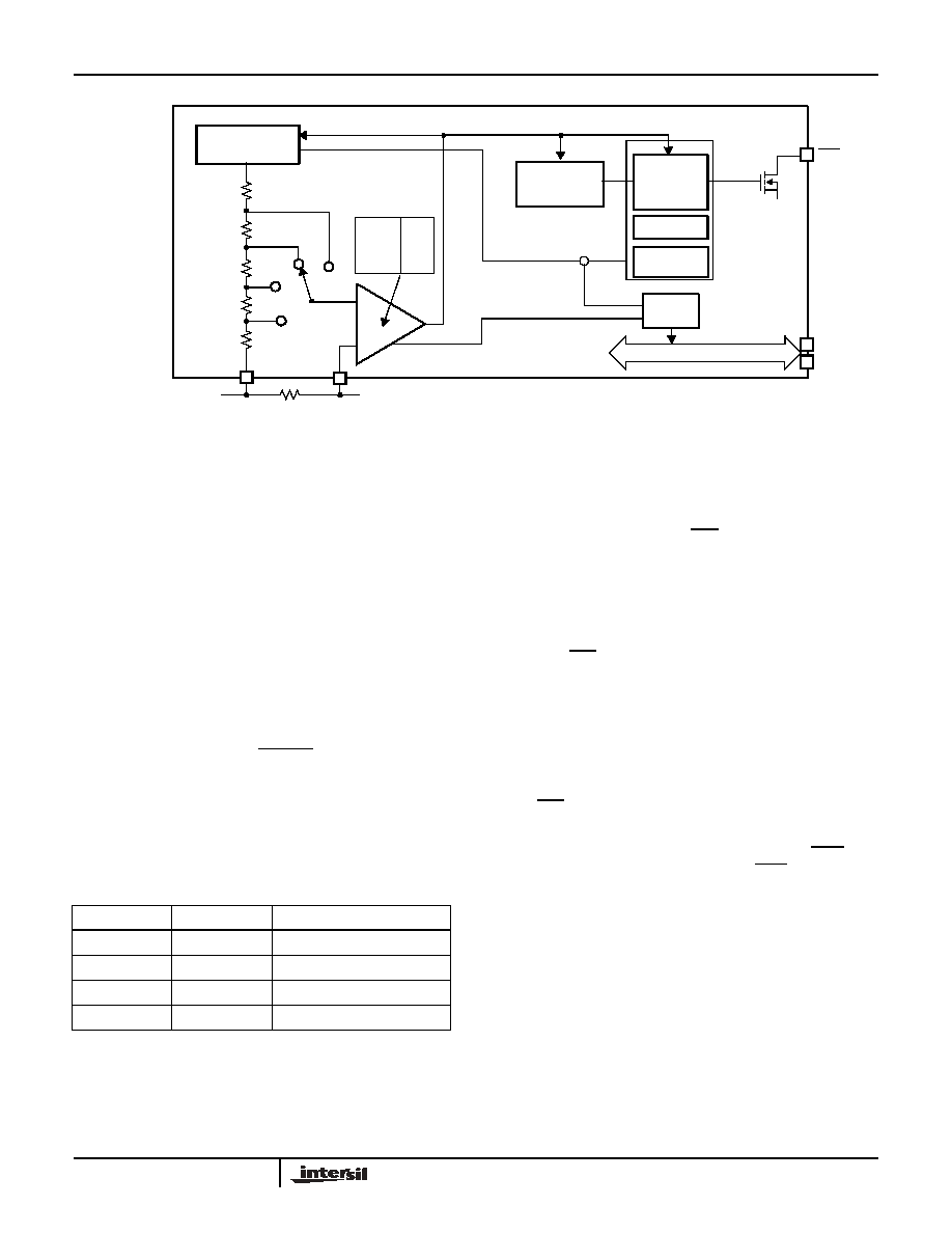
As shown in Figure 26, this circuit block contains
comparators and programmable voltage references to
monitor the single overvoltage and dual undervoltage trip
points. During manufacturing, Intersil programmed the
overvoltage and undervoltage trip points as shown in Table 1
below. Custom values are possible.
A resistor divider connected between the plus and minus
input voltages and the V
UV/OV
pin (see Figure 24)
determines the overvoltage and undervoltage shutdown
voltages and the operating voltage range. Using the
thresholds in Table 1 and the equations of Figure 24 the
desired operating voltage can be determined. Figure 25
shows the resistance values for various operating voltages.
Battery Back Up Operations
An external signal, BATT-ON, is provided to switch the
undervoltage trip point. The BATT-ON signal is a LOGIC
HIGH if V
IHB
> V
EE
+ 4V and is a LOGIC LOW if V
ILB
< V
EE
+ 2V. The time from a BATT-ON input change to a valid new
undervoltage threshold is 100ns. See Electrical
Specifications for more details.
Note: The V
UV/OV
pin must be limited to less than V
EE
+
5.5V in worst case conditions. Values for R1 and R2 must be
chosen such that this condition is met. Intersil recommends
R1 = 182k
and R2 = 10k to conform to factory settings.
Overvoltage/Undervoltage Fault Condition Flags
On any overvoltage or undervoltage violation, the X80000
cuts-off the GATE. This condition also sets the fault-
overvoltage (FOV) or fault-undervoltage1/2 (FUV1/2) bits
low. These bits are readable through the SMBus. To clear
the fault bits, the fault condition must first be rectified (by the
TABLE 1. OVERVOLTAGE/UNDERVOLTAGE DEFAULT
THRESHOLDS
THRESHOLD
SYMBOL
DESCRIPTION
FALLING
RISING
MAX/MIN
VOLTAGE
(Note 1)
LOCKOUT
VOLTAGE
(Note 2)
V
OV
Overvoltage
(X80000)
3.87V
3.9V
74.3
74.9
V
OV
Overvoltage
(X80001)
3.51V
3.54V
67.4
68
V
UV1
Undervoltage
1
2.21V
2.24V
43.0
42.4
V
UV2
Undervoltage
2
1.73V
1.76V
33.8
33.2
NOTES:
1. Max/Min Voltage is the maximum and minimum operating voltage
assuming the recommended V
UV/OV
resistor divider.
2. Lockout voltage is the voltage where the X80000/1 turns off the
FET.
TABLE 2. SELECTING BETWEEN UNDERVOLTAGE TRIP
POINTS
PIN
DESCRIPTION
TRIP POINT SELECTION
BATT-ON
Undervoltage Trip
Point Selection Pin
If BATT-ON = 0,
V
UV1
trip point is selected;
If BATT-ON = 1,
V
UV2
trip point is selected.
V
UV1
and V
UV2
are undervoltage thresholds.
R1
R2
V
P
V
UV/OV
V
N
Voltage divider:
or:
V
UV OV
/
V
S
R2
R1 R2
+
----------------------
=
V
S
V
UV OV
/
R1 R2
+
R2
----------------------
=
V
S
FIGURE 24. OVERVOLTAGE UNDERVOLTAGE DIVIDER
BATT-ON = V
EE
V
OV
V
UV1
V
UV2
Operating
Voltage
BATT-ON = V
RGO
100
90
80
70
60
50
40
30
20
10
0
150
158
166
175
182
190
198
206
214
222
O
P
ERA
T
IN
G V
O
L
T
A
G
E
(
V
)
R1 in k
(for R2=10K)
FIGURE 25. OPERATING VOLTAGE vs RESISTOR RATIO
X80000, X80001
18
FN8148.0
March 18, 2005
system) then cleared by a write to Fault Detection Register.
Please refer to FDR section. See Table 2.
Overcurrent Protection (Circuit Breaker Function)
The X80000 overcurrent circuit provides the following
functions:
∑ Overcurrent shut-down of the power FET and external
power good indicators.
∑ Noise filtering of the current monitor input.
∑ Relaxed overcurrent limits for initial board insertion.
∑ Overcurrent recovery retry operation.
∑ Flag of overcurrent fault condition.
∑ Flag of overcurrent retry failure.
A sense resistor, placed in the supply path between V
EE
and
SENSE (see Figure 22) generates a voltage internal to the
X80000. When this voltage exceeds 50mV, an over current
condition exists and an internal "circuit breaker" trips, turning
off the gate drive to the external FET. The actual overcurrent
level is dependent on the value of the current sense resistor.
For example a 20m
sense resistor sets the overcurrent
level to 2.5A.
Intersil's X80000 provides a safety mechanism during
insertion of the board into the back plane. During insertion of
the board into the backplane large currents may be induced.
In order to prevent premature shut down of the external FET,
the X80000 allows for a choice of up to 4 times the
overcurrent setting during insertion.
After the PWRGD signal is asserted, the X80000 switches
back to the normal overcurrent setting. The overcurrent
threshold voltage during insertion can be changed from
50mV to 100mV, 150mV, or 200mV, by setting bits in Control
Register CR4.
After the Power FET turns off due to an overcurrent
condition, a retry circuit turns the FET back on after a delay
of t
SC_RETRY
. If the overcurrent condition remains, the FET
again turns off. This sequence repeats until the overcurrent
condition is released. There are various other options that
program the retry circuit to change the number of retries or
to not retry. An optional output signal, FAR, indicates a
failure after retry.
Overcurrent Shut-down
As shown in Figure 27, this circuit block contains a resistor
ladder, a comparator, a noise filter and a programmable
voltage reference to monitor for overcurrent conditions.
The overcurrent voltage threshold (V
OC
) is 50mV. This can
be factory set, by special order, to any setting between
30mV and 100mV. V
OC
is the voltage between the SENSE
and V
EE
pins and across the R
SENSE
resistor. If the
selected sense resistor is 20m
, then 50mV corresponds to
an overcurrent of 2.5A.
If an overcurrent condition is detected, the GATE is turned
off, all power good indicators go inactive and an overcurrent
failure bit (FOC) is set.
Overcurrent Noise Filter
The X80000 has a noise (low pass) filter built into the
overcurrent comparator. The comparator will thus ignore
current spikes shorter than 5µs. Other filter options are
provided by setting control bits in register CR4. The control
bits set the comparator to ignore current spikes shorter that
5µs, 10µs or 20µs and allow the filter to be turned off.
TABLE 3. OVERVOLTAGE/UNDERVOLTAGE FLAG BITS
SYMBOL
VIOLATION (ON)
NORMAL (OFF)
FOV
FOV = 0, when
V
UV/OV
> V
OV
(Overvoltage)
FOV = 1, when
V
UV/OV
< V
OV
+ 0.2V
and reset by a write operation
FUV1/2
FUV1/2 = 0, when
V
UV/OV
< V
UV1/2
(Undervoltage)
FUV1/2 = 1, when
V
UV/OV
> V
UV1/2
- 0.2V
and reset by a write operation
Programmable
VREF
Control
& Status
Registers
2:1
Mux
-48V
V
UV/OV
BATT_ON
SDA
SCL
Overvoltage Flag
UV flag_1
UV flag_2
UV Fla
g
R1=182K
R2=10K
V
OV
To Gate
To Gate
Fault Bits
FOV
FUV1/2
+
-
-
+
-
+
Programmable
VREF
Programmable
VREF
V
UV1
V
UV2
SMBus
Control
Control
FIGURE 26. PROGRAMMABLE UNDERVOLTAGE AND
OVERVOLTAGE FOR PRIMARY AND BATTERY
BACKUP
TABLE 4. NOISE FILTER FOR OVER CURRENTS
F1
F0
t
NF
(maximum noise input pulse width)
0
0
0µs
0
1
5µs
1
0
10µs
1
1
20µs
X80000, X80001
19
FN8148.0
March 18, 2005
Overcurrent During Insertion
Insertion is defined as the first plug-in of the board to the
backplane. In this case, the X80000 is initially fully powered
off prior to the hot plug connection to the mains supply. This
condition is different from a situation where the mains supply
has temporarily failed resulting in a partial recycle of the
power. This second condition will be referred to as a power
cycle.
During insertion, the board can experience high levels of
current for short periods of time as power supply capacitors
charge up on the power bus. To prevent the overcurrent
sensor from turning off the FET inadvertently, the X80000
has the ability to allow more current to flow through the
powerFET and the sense resistor for a short period of time
until the FET turns on and the PWRGD signal goes active. In
the standard setting, 200mV is allowed across sense resistor
the during insertion (10A assuming a 20mW resistor). Two
bits in register CR4 select the insertion current limit of 1X,
2X, 3X or 4X the base setting of 50mV. This provides a
mechanism to reduce insertion issues associated with huge
current surges.
Hardshort Protection - Programmable Retry
In the event on an overcurrent or hard short condition, the
X80000 includes a retry circuit. This circuit waits for 100ms,
then attempts to again turn on the FET. If the fault condition
still exists, the FET turns off and a retry counter
(SC_Counter) increments. After the selected number of
failed trys, the X80000 sets a Failed After Retry Status
(FAR_STAT) fault bit, sets the FAR pin LOW and goes into
an idle state. In this state the GATE pin will not go active until
the device is cleared.
The retry circuit can be programmed to handle the retry
operation in one of eight ways (See Table 6). The options
allow retries from zero to unlimited and specifies when to
assert the FAR (Failure After Re-Try) signal. In the "Always
Retry" case there is no idle state, so when the overcurrent
condition clears, the GATE goes active and the FET turns
on.
There are four optional retry delay periods. These are
100ms, 500ms, 1s, and 5s. These are programmed by bits
located in the CR2 register.
After FAR is asserted, there are two ways to clear the
hardshort protection:
1. Master Reset Hot Side. The master reset pin, MRH, can
be asserted by pulling it LOW. Upon MRH assertion, all
default values are restored and the retry is cleared.
2. Power cycle the part, turning V
DD
OFF, then ON.
If an overcurrent condition does not occur on any retry, the
gate pin will proceed to open at the user defined slew rate.
Overcurrent Fault Condition Flags
On any overcurrent violation, the X80000 will cut-off the
GATE, turning off the voltage to the load, and setting all
power good pins to their disabled state. In this condition, the
fault-overcurrent bit (FOC) goes LOW. To clear FOC,
remove the over current condition, then write to the control
register. Refer to instructions on writing to the FDR (See
Table 8).
TABLE 5. INSERTION OVERCURRENT THRESHOLD OPTIONS
VS1
VS0
V
OCI
0
0
50mV (1X)
0
1
100mV (2X)
1
0
150mV (3X)
1
1
200mV (4X)
2 bit
noise
filtering
Control
Registers
SDA
SCL
Overcurrent
Logic and Gate
Control Block
Short-Circuit
Retry Logic
and System
Monitors
FAR
Failure After
Re-Try
Retry Delay
Retry Counter
N
retry
Fault Bit
FAR_STAT
Programmable
Voltage Reference
0µs
5µs
10µs
20µs
36R
4x
3x
2x
1x
R
R
R
R
+
≠
-48V
Overcurrent Event
R
Sense
SMBus
V
EE
FIGURE 27. OVERCURRENT DETECTION/SHORT CIRCUIT PROTECTION WITH PROGRAMMBLE RETRY AND FLAG MONITORS
X80000, X80001

20
FN8148.0
March 18, 2005
When exceeding the overcurrent retry limit, the status bit
"FAR_STAT" is set to `1' and the FAR pin is asserted. To
clear FAR_STAT, write to the control register. Refer to
instructions on writing to the FDR (See Table 9).
Gate Drive Output Slew Rate (Inrush Current)
Control
The gate output drives an external N-Channel FET. The
GATE pin goes high when no overcurrent, undervoltage or
overvoltage conditions exist.
The X80000 provides an I
GATE
current of 50µA to provide
on-chip slew rate control to minimize inrush current. This
current is programmable from 10µA to 160uA (in 10µA
steps) to allow the X80000 to support various load conditions
(See Figure 23 and Figure 28). I
GATE
is chosen to limit the
inrush current and to provide the best charge time for a
given load, while avoiding overcurrent conditions. The user
programs the I
GATE
current using four I
GATE
control bits.
For applications that require different ramp rates during
insertion and start-up and operations modes, the X80000
provides two external pins, IGQ1 and IGQ0, that allow the
user to switch to different GATE currents on-the-fly by
selecting one of four pre-selected I
GATE
currents. When
IGQ0 and IGQ1 are left unconnected, the gate current is
determined by the gate control bits. The other three settings
are 10µA, 70µA and 150µA. Typically, the delay from IGQ1
and IGQ0 selection to a change in the GATE pin current is
less than 1
µsecond.
Programmable Slew Rate (Gate) Control
As shown in Figure 29, this circuit block contains a
selectable current source (I
GATE
) that drives the 50µA
current into the GATE pin. This current provides a controlled
slew rate for the FET.
X80000 allows the user to change the gate current to one of
sixteen possible I
GATE
values. The options allow currents of
between 10
µA to 160µA in 10µA increments.
Once the overcurrent condition and the amount of load is
known, an appropriate slew rate can be determined and
selected for the external FET. This will ensure proper
TABLE 6. RETRY AND EVENT SEQUENCE OPTIONS
NR2 NR1 NR0
N
RETRY
AND RETRY SEQUENCE OF EVENTS
(FAILURE MODE)
0
0
0
Always Retry, Do Not assert FAR pin (Default)
0
0
1
N
RETRY
= 1 (one retry), assert FAR pin after
N
RETRY,
STOP retry, and shutoff GATE pin
0
1
0
N
RETRY
= 2 (two retries), assert FAR pin after
N
RETRY,
STOP retry, and shutoff GATE pin
0
1
1
N
RETRY
= 3 (three retries), assert FAR pin after
N
RETRY,
STOP retry, and shutoff GATE pin
1
0
0
N
RETRY
= 4 (four retries), assert FAR pin after
N
RETRY,
STOP retry, and shutoff GATE pin
1
0
1
N
RETRY
= 5 (five retries), assert FAR pin after
N
RETRY,
STOP retry, and shutoff GATE pin
1
1
0
Always Retry, assert FAR pin after 1st retry; clear
FAR when FOC cleared, do not shutoff GATE
pin.
1
1
1
N
RETRY
= 0 (no retry), asset FAR, and shutoff
GATE pin.
TABLE 7. RETRY EVENT DELAY OPTIONS
TSC1
TSC0
t
SC_RETRY
,
DELAY BETWEEN RETRIES
0
0
100 miliseconds
0
1
500 miliseconds
1
0
1 second
1
1
5 seconds
TABLE 8. OVERCURRENT FLAG BIT
STATUS
BIT
VIOLATION (ON)
NORMAL (OFF)
FOC
FOC = 0, when
V
RSENSE
> V
OC
FOC = 1, when:
V
RSENSE
< V
OC
- 0.2V
and reset by a write operation
or hardshort retry is initiated.
TABLE 9. RETRY COUNT FAILURE STATUS BIT
STATUS BIT
CONDITION
FAR_STAT
if FAR_STAT = 1, FAR is asserted.
if FAR_STAT = 0, FAR is deasserted
INR
U
SH CURRENT
Overcurrent
I
GATE
I
GATE
= 160µA
100µA
75µA
25µA
10µA
T1
TIME (ms)
T2
T3
T4
T5
FIGURE 28. SELECTING I
GATE
CURRENT FOR SLEW RATE
CONTROL ON THE GATE PIN
X80000, X80001
21
FN8148.0
March 18, 2005
operation to control Inrush currents during hot insertion
modes.
Software Slew Rate Control
Users can adjust the slew rate control by using an SMBus
write command to change the slew rate control bits. This
allows adaptation in the case of changing load conditions,
creates a modular design for downstream DC-DC supplies,
and provides control of the load on the hot voltage when
slew rates vs. loads vary.
Gate Capacitor, Filtering and Feedback
In Figure 29, the FET control circuit includes an FET
feedback capacitor C
2
, which provides compensation for the
FET during turn on. The capacitor value depends on the
load, the FET gate current, and the maximum desired inrush
current.
The value of C2 can be selected with the following formula:
Where:
I
GATE
= FET Gate current
I
INRUSH
= Maximum desired inrush current
C
LOAD
= DC/DC bulk capacitance
With the X80000, there is some control of the gate current
with the IGQ pins and IGx bits, so one selection of C2 can
cover a wide range of possible loading conditions. Typical
values for C2 range from 2.2 to 4.7nF.
When power is applied to the system, the FET tries to turn
on due to its internal gate to drain capacitance (Cgd) and the
feedback capacitor C2 (see Figure 29). The X80000 device,
when powered, pulls the gate output low to prevent the gate
voltage from rising and keep the FET from turning on.
However, unless V
DD
powers up very quickly, there will be a
brief period of time during initial application of power when
the X80000 circuits cannot hold the gate low. The use of an
external capacitor (C1) prevents this. Capacitors C1 and C2
form a voltage divider to prevent the gate voltage from rising
above the FET turn on threshold before the X80000 can hold
the gate low. Use the following formula for choosing C1.
Where:
V1 = Maximum input voltage,
V2 = FET threshold Voltage,
C1 = Gate capacitor,
C2 = Feedback capacitor.
In a system where V
DD
rises very fast, a smaller value of C1
may suffice as the X80000 will control voltage at the gate
before the voltage can rise to the FET turn on threshold. The
circuit of Figure 29 assumes that the input voltage can rise to
80V before the X80000 sees operational voltage on V
DD
. If
C1 is used then the series resistor R1 will be required to
prevent high frequency oscillations.
GATE Current Quick Selection
For applications that require different ramp rates during
insertion and start-up and operations modes or those where
the serial interface is not available, the X80000 provides two
SENSE
V
EE
R
SENSE
LOAD
V
DD
=12V
Slew
Selection
GATE
10µA
I
INRUSH
DRAIN
100K
Gate Current
IGQ1
IGQ0
-48V
Control
Registers
SDA
SCL
SMBus
to
160µA
Logic
Rate
Quick Select
Logic
100*
100nF*
* Optional Components
See Section "Gate Capacitor, Filtering and Feedback"
22K
3.3nF
C2
R2
FIGURE 29. PROGRAMMBLE SLEW RATE (INRUSH
CURRENT) CONTROL
C2
I
GATE
C
◊
LOAD
I
INRUSH
-------------------------------------------
=
TABLE 10. I
GATE
OUTPUT CURRENT OPTIONS
IG3
IG2
IG1
IG0
I
GATE
(
µA)
0
0
0
0
10
0
0
0
1
20
0
0
1
0
30
0
0
1
1
40
0
1
0
0
50
Default
0
1
0
1
60
0
1
1
0
70
0
1
1
1
80
1
0
0
0
90
1
0
0
1
100
1
0
1
0
110
1
0
1
1
120
1
1
0
0
130
1
1
0
1
140
1
1
1
0
150
1
1
1
1
160
C1
V1
V2
≠
V2
--------------------- C2
=
X80000, X80001

22
FN8148.0
March 18, 2005
external pins, IGQ1 and IGQ0, that allow the system to
switch to different GATE current on-the-fly with pre-selected
I
GATE
currents.
The IGQ1 and IGQ0 pins can be used to select from one of
four set values.
Typically, the delay from IGQ1 and IGQ0 selection to a
change in the GATE pin current is less than 1
µsecond.
Drain Sense and Power Good Indicator
The X80000 provides a drain sense and power good
indicator circuit. The PWRGD signal asserts LOW when
there is no overvoltage, no undervoltage, and no overcurrent
condition, the Gate voltage exceeds VDD-1V, and the
voltage at the DRAIN pin is less V
EE
+V
DRAIN
.
As shown in Figure 30, this circuit block contains a drain
sense voltage trip point (
V
DRAIN
) and a gate voltage trip
point (
V
GATE
), two comparators, and internal voltage
references. These provide both a drain sense and a gate
sense circuit to determine the whether the FET has turned
on as requested. If so, the power good indicator (PWRGD)
goes active.
The drain sense circuit checks the DRAIN pin. If the voltage
on this pin is greater that 1V above V
EE
, then a fault
condition exists.
The gate sense circuit checks the GATE pin. If the voltage
on this pin is less than V
EE
- 1V, then a fault condition exists.
The PWRGD signal asserts (Logic LOW) only when all of the
below conditions are true:
∑ there is no overvoltage or no undervoltage condition, (i.e.
undervoltage < V
EE
< overvoltage.)
∑ There is no overcurrent condition (i.e. V
EE
- V
SENSE
<
V
OC
.)
∑ The FET is turned on (i.e. V
DRAIN
< V
EE
+ 1V and V
GATE
> V
DD
- 1V).
Power On Reset and System Reset With Delay
Application of power to the X80000 activates a Power On
Reset circuit that pulls the RESET pin active. This signal, if
used, provides several benefits.
∑ It prevents the system microprocessor from starting to
operate with insufficient voltage.
∑ It prevents the processor from operating prior to
stabilization of the oscillator.
∑ It allows time for an FPGA to download its configuration
prior to initialization of the circuit.
∑ It prevents communication to the EEPROM during
unstable power conditions, greatly reducing the likelihood
of data corruption on power up.
The SPOR/RESET circuit is activated when all voltages are
within specified ranges and the following time-out conditions
are met: PWRGD and V1GOOD, V2GOOD, V3GOOD, and
V4GOOD. The SPOR/RESET circuit will then wait 100ms
and assert the RESET pin. The SPOR delay may be
changed by setting the TPOR bits in register CR2. The delay
can be set to 100 ms, 500 ms, 1 second, or 5 seconds.
IGQ1
PIN
IGQ0
PIN
CONTENTS
0
0
Defaults to gate current set by IG3:IG0 bits
0
1
Gate Current is 10
µA
1
0
Gate Current is 70
µA
1
1
Gate Current is 150
µA
TABLE 11. SPOR RESET DELAY OPTIONS
TPOR1
TPOR0
t
SPOR
DELAY BEFORE RESET
ASSERTION
0
0
100 miliseconds (default)
0
1
500 miliseconds
1
0
1 second
1
1
5 seconds
(Factory
Programmable)
SENSE
V
EE
R
SENSE
LOAD
GATE
DRAIN
100K
-48V
SDA
SCL
SMBus
PWRGD
+
≠
1V
V
EE
Control/Status
Registers
Power
Good
Logic
V
DRAIN
+
≠
VDD-1V
V
GATE
FIGURE 30. DRAIN SENSE AND POWER GOOD INDICATOR
X80000, X80001

23
FN8148.0
March 18, 2005
Quad Voltage Monitoring
X80000 monitors 4 voltage enable inputs. When the ENi
(i=1-4) input is detected to be below the input threshold, the
output ViGOOD (i = 1 to 4) goes active. The ViGOOD signal
is asserted after a delay of 100ms. This delay can be
changed on each ViGOOD output individually with bits in
register CR3. The delay can be 100ms, 500ms, 1s and 5s.
The ViGOOD signal remains active low until ENi rises above
threshold.
Once the PWRGD signal is asserted, the power sequencing
of the DC-DC modules can commence. RESET will go active
100ms after all ViGOOD (i=1 to 4) outputs are asserted. This
delay time can be changed by setting bits in register CR2
(See Figure 32).
As shown in Figure 32, this circuit block contains four
separate voltage enable inputs, a time delay circuit, and an
output driver.
Manual Reset and Remote Shutdown
The manual reset option allows a hardware reset of either
the Gate control or the PWRGD indicator. These can be
used to recover the system in the event of an abnormal
operating condition.
The remote shutdown feature of the X80000 allows smart
power control remotely through the SMBus. The host system
can either override the control of the FET, thus turning it off,
or it can remove the override. Removing the override restarts
the power up sequence.
The X80000 has two manual reset pins: MRH (manual reset
hot side) and MRC (manual reset cold side). The MRH
signal is used as a manual reset for the GATE pin. This pin is
used to initiate Soft Reinsert. When MRH is pulled LOW the
GATE pin will be pulled LOW. It also clears the Remote
Shutdown Register (RSR) and the FAR signal. When the
MRH pin goes HIGH, it removes the override signal and the
Control
Registers
EEPROM
2Kbits
RESET Logic
SPOR
MRC
SDA
V
DD
Drain Sense
& Power
Good Logic
Enable
Logic
t
SPOR
Delay
RESET
PWRGD
ViGOOD
i = 1 to 4
µ
P
Bus I
n
ter
f
ac
e
SCL
V
EE
Remote
& Fault
FIGURE 31. POWER ON/SYSTEM RESET AND DELAY
(BLOCK DIAGRAM)
TABLE 12. ViGOOD OUTPUT TIME DELAY OPTIONS
TiD1
TiD0
t
DELAYi
0
0
100ms
0
1
500ms
1
0
1 secs
1
1
5 secs
where i is the ith voltage enable (i = 1 to 4).
EN1
EN2
EN3
EN4
V4GOOD
V3GOOD
V2GOOD
V1GOOD
V
EE
Divider
4
Reset
OSC
0.1s
0.5s
1s
5s
Select
4
delay1
delay2
delay3
delay4
Delay circuit
repeated 4 times
V
RGO
Control Register
SMBus Interface
Fault Detection Register
FIGURE 32. VOLTAGE ENABLE CONTROL AND VGOOD OUTPUTS
X80000, X80001

24
FN8148.0
March 18, 2005
gate will turn on based on the selected gate control
mechanism.
The MRC signal is used as a manual reset for the PWRGD
signal. This pin is used to initiate a Soft Restart. When the
MRC is pulled HIGH, the PWRGD signal is pulled HIGH.
When MRC pin goes LOW, the PWRGD pin goes low using
the MRC pin has no affect on the FET gate control, so the
FET remains on.
Fault Detection
The X80000 contains a Fault Detection Register (FDR) that
provides the user the status of the causes for a RESET pin
active (See Table 17).
At power-up, the FDR is defaulted to all "0". The system
needs to initialize the register to all "1" before the actual
monitoring can take place. In the event that any one of the
monitored sources fail, the corresponding bit in the register
changes from a "1" to a "0" to indicate the failure (ViGOOD
sources set the bit LOW when the ViGOOD goes LOW
indicating a "good" status). When a RESET is detected by
the main controller, the controller should read of the FDR
and note the cause of the fault. After reading the register, the
controller can reset the register bit back to all "1" in
preparation for future monitored conditions.
Remote Shutdown
The gate of the external MOSFET can be remotely shutdown
by using a software command sequence. A byte write of
`10101010' (AAh) data to the Remote Shutdown Register
(RSR) will shutdown the gate and the gate will be pulled low.
Activating the MRH pin or a writing 00h into the RSR will turn
off the override signal and the gate will turn on based on the
gate control mechanism.
The RSR powers up with `0's in the register and its contents
are volatile.
Flexible Power Sequencing of Multiple Power
Supplies
The X80000 provides several circuits such as multiple
voltage enable pins, programmable delays, and a power
good signals that can be used to set up flexible power
sequencing schemes for downstream DC-DC supplies.
Below are two examples:
1. Power Up of DC-DC Supplies In Parallel Sequencing
Using Programmable Delays on Power Good (See Figure
33 and Figure 34).
Several DC-DC power supplies and their respective
power up start times can be controlled using the X80000
such that each of the DC-DC power supplies will start up
following the issue of the PWRGD signal. The PWRGD
signal is fed into the ENi inputs to the X80000. When
PWRGD is valid, the internal voltage enable inputs issue
ViGOOD signals after a time delay. The ViGOOD signals
control the ON/OFF pins of the DC-DC supplies. In the
factory default condition, each DC/DC converter is
instructed to turn on 100ms after the PWRGD goes
active. However, each ViGOOD delay is individually
selectable as 100ms, 500ms, 1s and 5s. The delay times
are changed via the SMBus during calibration of the
system.
2. Power Up of DC-DC Supplies Via Relay Sequencing
Using Power Good and Voltage Enables (see Figure 35
and Figure 36).
Several DC-DC power supplies and their respective
power up start times can be controlled using the X80000
such that each of the DC-DC power supplies will start in
a relay sequencing fashion. The 1st DC-DC supply will
power up when PWRGD is LOW after a 100ms delay.
Subsequent DC-DC supplies will power up after the prior
supply has reached its operating voltage. One way to do
this is by using an external CPU Supervisor (for example
the Intersil X40430) to monitor the DC-DC output. When
the DC/DC voltage is good, the supervisor output signals
the X80000 EN1 input to sequence the next supply. An
opto-coupler is recommended in this connection for
isolation. This configuration ensures that each
subsequent DC-DC supply will power up after the
preceding DC-DC supplys voltage output is valid. Again,
the X80000 offers programmable delays for each voltage
enable input that is selectable via the SMBus during
calibration of the system.
TABLE 13. MANUAL RESET OF THE HOT SIDE (GATE SIGNAL)
MRH
GATE PIN
REQUIREMENTS
1
Operational When
MRH is HIGH the Manual Reset (Hot)
function is disabled and the
device operates normally
0
OFF
MRH must be held LOW minimum of 5
µsecs
to turn of the GATE
TABLE 14. MANUAL RESET OF THE COLD SIDE (PWRGD
SIGNAL)
MRC
PWRGD
Requirements
1
HIGH
MRC must be held HIGH minimum of 5
µsecs
to set PWRGD HIGH
0
Operational When
MRC
is
LOW the MRC function is
disabled and the device operates normally
X80000, X80001
25
FN8148.0
March 18, 2005
V
DD
V3GOOD
EN3
V2GOOD
EN2
V1GOOD
EN1
PWRGD
X80000
V
UV/OV
V
EE
SENSE
DRAIN
-48V
UV=37V
OV=71V
-48V
GATE
Rs
0.02
5%
ON/OFF
C3
0.1µF
100V
C4
100µF
100V
1
4
V
IN+
V
IN-
V
OUT
+
V
OUT
SENSE+
TRIM
SENSE-
+
9
8
7
6
5
RESET
µC
V
CC1
3.3V
ON/OFF
C6
0.1µF
100V
C7
100µF
100V
1
4
V
IN+
V
IN-
V
OUT
+
V
OUT
SENSE+
TRIM
SENSE-
+
9
8
7
6
5
FPGA
V
CC1
2.5V
ON/OFF
C9
0.1µF
100V
C10
100µF
100V
1
4
V
IN+
V
IN-
V
OUT
+
V
OUT
SENSE+
TRIM
SENSE-
+
9
8
7
6
5
ASIC
V
CC1
1.8V
R4
182K
1%
R5
30K
1%
R6
10K
1%
Q1
IRFR120
C5
100µF
16V
C8
100µF
16V
C11
100µF
16V
+
+
+
V4GOOD
EN4
ON/OFF
C12
0.1µF
100V
C13
100µF
100V
1
4
V
IN+
V
IN-
V
OUT
+
V
OUT
SENSE+
TRIM
SENSE-
+
9
8
7
6
5
1.2V
C14
100µF
16V
+
RESET
OPTO
COUPLER
PWRGD
RESET
V
CC2
V
CC2
V
CC2
MRH
MRC
Return
100K
OPTO
COUPLER
X80001
0.1µF
100
4.7K
3.3n
-48V
Return
-48V
Return
-48V
Return
-48V
Return
FIGURE 33. TYPICAL APPLICATION OF HOTSWAP AND DC-DC PARALLEL POWER SEQUENCING
X80000, X80001
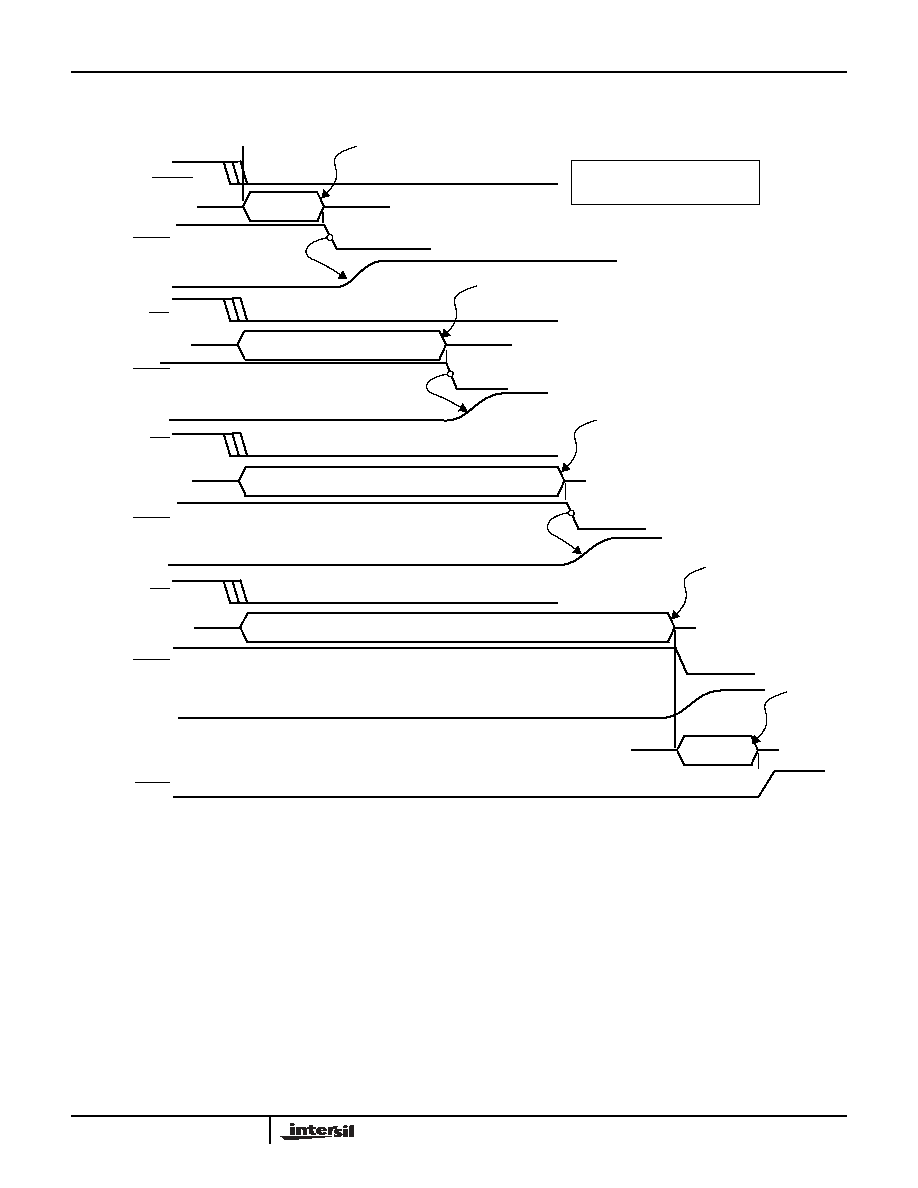
26
FN8148.0
March 18, 2005
EN2 In
t
DELAY1
V1GDO
Power Supply
#1 turns ON
Power Supply
Power Supply
#3 turns ON
V2GDO
100ms
V3GDO
Programmable
Delay
Programmable
Delay
#1 OUTPUT
500ms
1sec
5sec
100ms
500ms
1sec
5sec
t
DELAY2
Power Supply
#2 turns ON
100ms
500ms
1sec
5sec
t
DELAY3
Power Supply
#2 OUTPUT
Power Supply
#3 OUTPUT
t
DELAY4
Programmable
Delay
V4GDO
(from PWRGD)
(3.3V)
(2.5V)
(1.8V)
t
RESET
Programmable
Delay
RESET
100ms
500ms
1sec
5sec
100ms
500ms
1sec
5sec
FET
turns ON
Select t
DELAYx
and t
RESET
via the 2-wire interface.
EN2
EN3
Power Supply
#4 OUTPUT
(1.2V)
EN4
Programmable
Delay
Power Supply
#4 turns ON
FIGURE 34. PARALLEL SEQUENCING OF DC-DC SUPPLIES (TIMING)
X80000, X80001
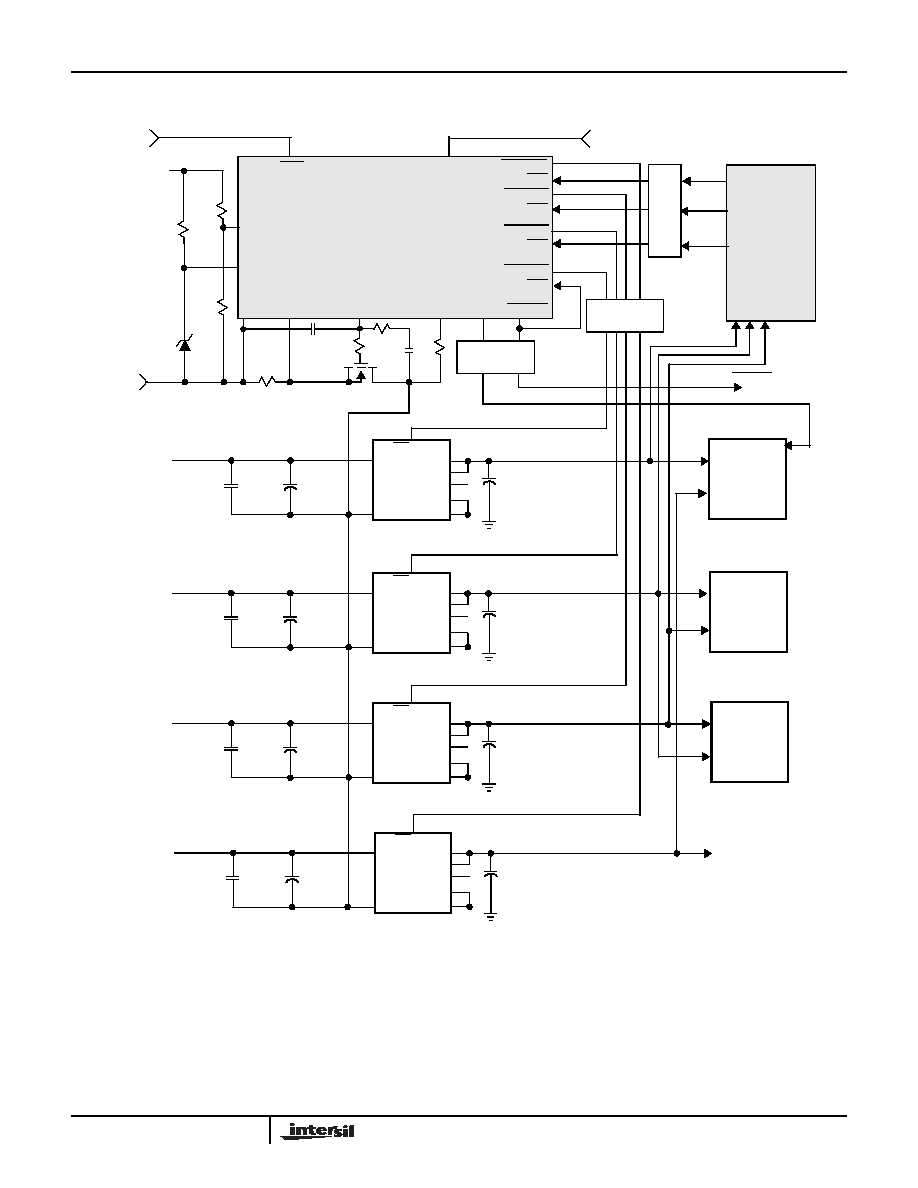
27
FN8148.0
March 18, 2005
V
DD
V3GOOD
EN3
V2GOOD
EN2
V1GOOD
EN1
PWRGD
X80000
V
UV/OV
V
EE
SENSE
DRAIN
-48V
UV=37V
OV=71V
-48V
GATE
Rs
0.02
5%
ON/OFF
C3
0.1µF
100V
C4
100µF
100V
1
4
V
IN+
V
IN-
V
OUT
+
V
OUT
SENSE+
TRIM
SENSE-
+
9
8
7
6
5
3.3V
ON/OFF
C6
0.1µF
100V
C7
100µF
100V
1
4
V
IN+
V
IN-
V
OUT
+
V
OUT
SENSE+
TRIM
SENSE-
+
9
8
7
6
5
2.5V
ON/OFF
C9
0.1µF
100V
C10
100µF
100V
1
4
V
IN+
V
IN-
V
OUT
+
V
OUT
SENSE+
TRIM
SENSE-
+
9
8
7
6
5
1.8V
R4
182k
1%
R6
10k
1%
Q1
IRFR120
C5
100µF
16V
C8
100µF
16V
C11
100µF
16V
+
+
+
V4GOOD
EN4
ON/OFF
C12
0.1µF
100V
C13
100µF
100V
1
4
V
IN+
V
IN-
V
OUT
+
V
OUT
SENSE+
TRIM
SENSE-
+
9
8
7
6
5
1.2V
C14
100µF
16V
+
RESET
OP
T
O
COUP
LER
RESET
X40430
OPTO
COUPLER
VMON<1:3>
VF
A
I
L<1:3
>
PWRGD
RESET
µC
V
CC1
FPGA
V
CC1
ASIC
V
CC1
V
CC2
V
CC2
V
CC2
MRH
MRC
R5
30k
1%
Return
100K
OPTO
COUPLER
X80001
(Optional)
0.1µF
100
4.7K
3.3n
-48V
Return
-48V
Return
-48V
Return
-48V
Return
FIGURE 35. TYPICAL APPLICATION OF HOTSWAP AND DC-DC RELAY SEQUENCING
X80000, X80001

28
FN8148.0
March 18, 2005
Control Registers and Memory
The user addressable internal control, status and memory
components of the X80000 can be split up into four parts:
∑ Control Register (CR)
∑ Fault Detection Register (FDR)
∑ Remote Shutdown Register (RSR)
∑ EEPROM array
Registers
The Control Registers, Remote Shutdown Register and
Fault Detection Register are summarized in Table 15.
Changing bits in these registers change the operation of the
device or clear fault conditions. Reading bits from these
registers provides information about device configuration or
fault conditions. Reads and writes are done through the
SMBus serial port. It is important to remember that, in most
cases, the SMBus serial port must be isolated between the
X80000, which is referenced to -48V, and the system
controller, which is referenced to ground.
EN2 In
t
DELAY1
V1GDO
Power Supply
#1 turns ON
Power Supply
V2MON
threshold
Power Supply
#3 turns ON
V2GDO
100ms
V3GDO
Programmable
Delay
Programmable
Delay
#1 OUTPUT
500ms
1sec
5sec
100ms
500ms
1sec
5sec
t
DELAY2
Power Supply
#2 turns ON
V3MON
threshold
100ms
500ms
1sec
5sec
t
DELAY3
Programmable
Delay
Power Supply
#2 OUTPUT
V4MON
Power Supply
#3 OUTPUT
threshold
t
DELAY4
Programmable
Delay
V4GDO
(from PWRGD)
(3.3V)
(2.5V)
(1.8V)
t
RESET
Programmable
Delay
RESET
100ms
500ms
1sec
5sec
100ms
500ms
1sec
5sec
FET
turns ON
Select t
DELAYx
and t
RESET
via the 2-wire interface.
EN2
EN3
Power Supply
#4 OUTPUT
(1.2V)
EN4
Power Supply
#4 turns ON
FIGURE 36. RELAY SEQUENCING OF DC-DC SUPPLIES (TIMING)
X80000, X80001
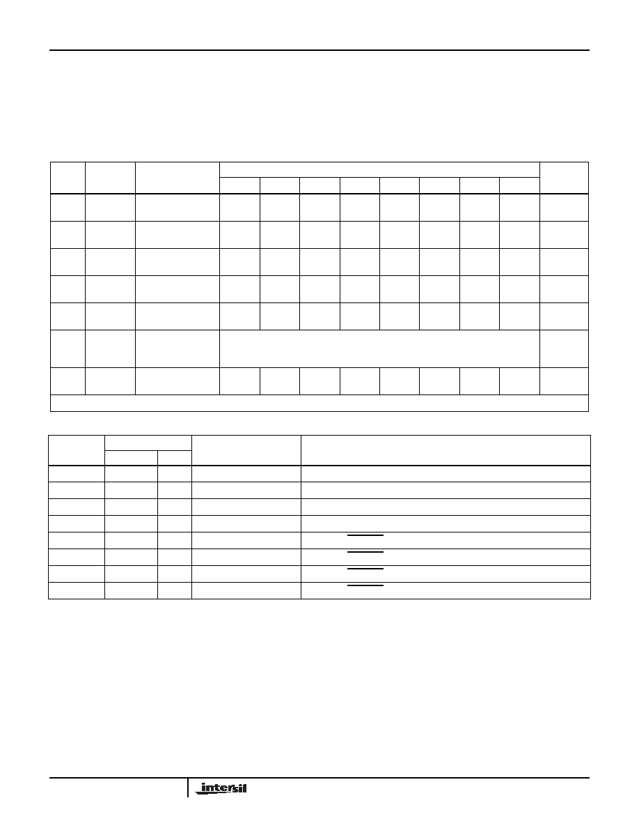
29
FN8148.0
March 18, 2005
All of the Control Register bits are nonvolatile (except for the
WEL bit), so they do not change when power is removed.
The values of the Register Block can be read at any time by
performing a random read (see Serial Interface) at the
specific byte address location. Only one byte is read by each
register read operation.
Bits in the registers can be modified by performing a single
byte write operation directly to the address of the register
and only one data byte can change for each register write
operation.
TABLE 15. REGISTER ADDRESS MAP
BYTE
ADDR.
REGISTER
NAME
DESCRIPTION
BIT
MEMORY
TYPE
7
6
5
4
3
2
1
0
00H
CR0
Control
Register 0
WEL
0
0
0
0
0
0
0
Volatile
01H
CR1
Control
Register 1
WPEN
0
0
BP1
BP0
NR2
NR1
NR0
EEPROM
02H
CR2
Control
Register 2
IG3
IG2
IG1
IG0
TPOR1
TPOR0
TSC1
TSC0
EEPROM
03H
CR3
Control
Register 3
T4D1
T4D0
T3D1
T3D0
T2D1
T2D0
T1D1
T1D0
EEPROM
04H
CR4
Control
Register 4
VS1
VS0
F1
F0
0
0
0
0
EEPROM
05H
RSR
(Note 1)
Remote Shutdown
Register
AAh: Override FET control and shutdown the FET
00h: Turn off override
(All other data combinations to RSR are reserved.)
Volatile
FF
FDR
Fault Detection
Register
FOV
FUV1/2
FOC
FAR_
STAT
V40S
V30S
V20S
V10S
Volatile
(1) This register is write only
TABLE 16. FAULT DETECTION BITS SUMMARY
SYMBOL
LOCATION(S)
CONTROL FUNCTION/
STATUS INDICATION
DESCRIPTION
REGISTER
BITS
FAR_STAT
FDR
4
Retry Violation
FAR_STAT = 0 : Failure After retry detected (must be preset to 1).
FOC
FDR
5
Overcurrent Violation
FOC = 0 : Over current detected (must be preset to 1).
FOV
FDR
7
Overvoltage Violation
FOV = 0 : Over voltage detected (must be preset to 1).
FUV1/2
FDR
6
Undervoltage Violation
FUV1/2 = 0 : Under voltage detected (must be preset to 1).
V1OS
FDR
0
1st Voltage Good
V1OS = 0 : V1GOOD pin has been asserted (must be preset to 1).
V2OS
FDR
1
2nd Voltage Good
V2OS = 0 : V2GOOD pin has been asserted (must be preset to 1).
V3OS
FDR
2
3rd Voltage Good
V3OS = 0 : V3GOOD pin has been asserted (must be preset to 1).
V4OS
FDR
3
4th Voltage Good
V4OS = 0 : V4GOOD pin has been asserted (must be preset to 1).
X80000, X80001
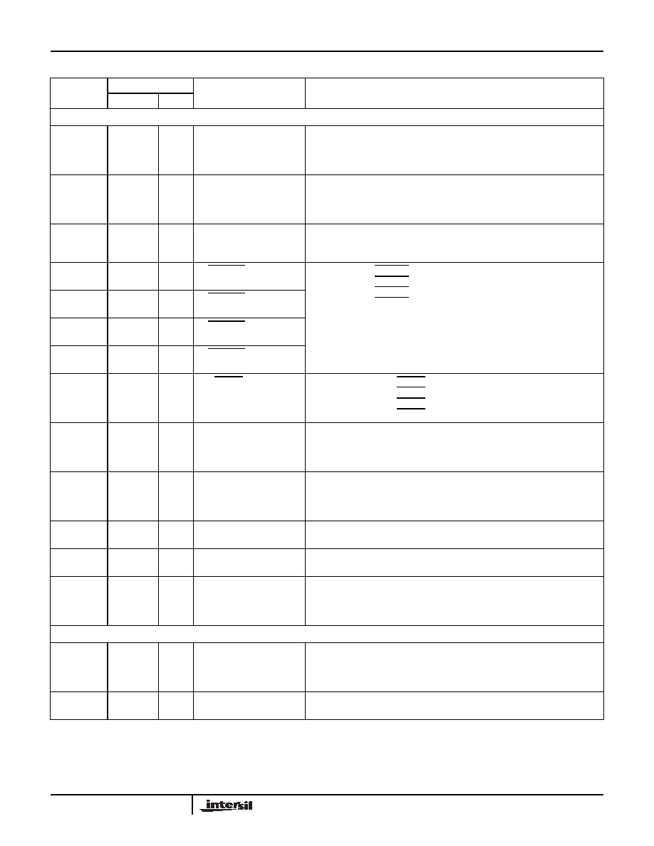
30
FN8148.0
March 18, 2005
TABLE 17. HARDWARE/SOFTWARE CONTROL AND FAULT DETECTION BITS SUMMARY
SYMBOL
LOCATION(S)
CONTROL FUNCTION/
STATUS INDICATION
DESCRIPTION
REGISTER
BITS
SOFTWARE CONTROL BITS
F0
F1
CR4
5:4
Insertion Current Filter
F1=0, F0=0 ; t
NF
= 0
F1=0, F0=1 ; t
NF
= 5µs
F1=1, F0=0 ; t
NF
= 10µs
F1=1, F0=1 ; t
NF
= 20µs
IG0
IG1
IG2
IG3
CR2
7:4
Gate Current Select
See Table 10.
NR0
NR1
NR2
CR1
2:0
Retry Sequence Options
See Table 6.
T1D0
T1D1
CR3
1:0
V1GOOD Time Delay
TiD1=0, TiD0=0 : ViGOOD delay = 100ms
TiD1=0, TiD0=1 : ViGOOD delay = 500ms
TiD1=1, TiD0=0 : ViGOOD delay = 1s
TiD1=1, TiD0=1 : ViGOOD delay = 5s
T2D0
T2D1
CR3
3:2
V2GOOD Time Delay
T3D0
T3D1
CR3
5:4
V3GOOD Time Delay
T4D0
T4D1
CR3
7:6
V4GOOD Time Delay
TPOR0
TPOR1
CR2
3:2
RESET delay time
TPOR1=0, TPOR0=0 : RESET delay = 100ms
TPOR1=0, TPOR0=1 : RESET delay = 500ms
TPOR1=1, TPOR0=0 : RESET delay = 1s
TPOR1=1, TPOR0=1 : RESET delay = 5s
TSC0
TSC1
CR2
1:0
Overcurrent Retry Delay
Time
TSC1=0, TSC0=0 ; t
SC_RETRY
= 100ms
TSC1=0, TSC0=1 ; t
SC_RETRY
= 500ms
TSC1=1, TSC0=0 ; t
SC_RETRY
= 1s
TSC1=1, TSC0=1 ; t
SC_RETRY
= 5s
VS0
VS1
CR4
7:6
Insertion Overcurrent Limit VS1=0, VS0=0 ; Insertion Overcurrent Limit = 1X
VS1=0, VS0=1 ; Insertion Overcurrent Limit = 2X
VS1=1, VS0=0 ; Insertion Overcurrent Limit = 3X
VS1=1, VS0=1 ; Insertion Overcurrent Limit = 4X
WEL
CR0
7
Write Enable
WEL = 1 enables write operations to the control registers and EEPROM.
WEL = 0 prevents write operations.
WPEN
CR1
7
Write Protect
WPEN = 1 (and WP pin HIGH) prevents writes to the control registers and the
EEPROM.
BP1
BP0
CR1
4:3
EEPROM Block Protect
BP1=0, BP0=0 : No EEPROM memory protected.
BP1=0, BP0=1 : Upper 1/4 of EEPROM memory protected
BP1=1, BP0=0 : Upper 1/2 of EEPROM memory protected.
BP1=1, BP0=1 : All of EEPROM memory protected.
HARDWARE SELECT BITS
IGQ0
IGQ1
Input pins
Gate Current Select
IGQ1=0, IGQ0=0 : I
GATE
= set by IG0-IG3
IGQ1=0, IGQ0=1 : I
GATE
= 10µA
IGQ1=1, IGQ0=0 : I
GATE
= 70µA
IGQ1=1, IGQ0=1 : I
GATE
= 150µA
BATTON
Input pin
Main or Battery
BATTON = 0 ; Undervoltage Threshold = V
UV1
BATTON = 1 ; Undervoltage Threshold = V
UV2
X80000, X80001
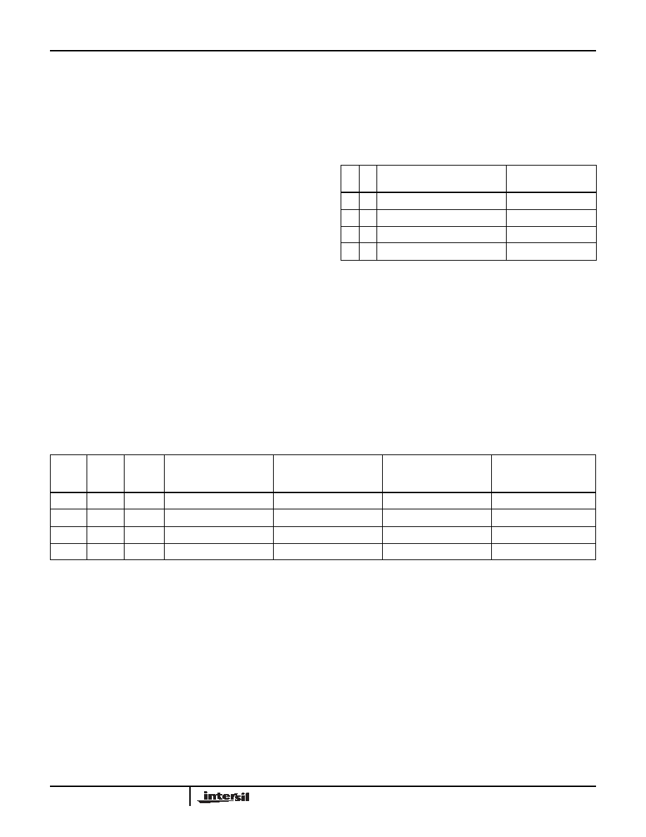
31
FN8148.0
March 18, 2005
Memory
The X80000 contains a 2kbit EEPROM memory array. This
array can contain information about manufacturing location
and dates, board configuration, fault conditions, service
history, etc. Access to this memory is through the SMBus
serial port. Read and write operations are similar to those of
the control registers, but a single command can write up to
16 bytes at one time. A single read command can return the
entire contents of the EEPROM memory.
Register and Memory Protection
In order to reduce the possibility of inadvertent changes to
either a control register of the contents of memory, several
protection mechanisms are built into the X80000. These are
a Write Enable Latch, Block Protect bits, a Write Protect
Enable bit and a Write Protect pin.
WEL: Write Enable Latch
A write enable latch (WEL) bit controls write accesses to the
nonvolatile registers and the EEPROM memory array in the
X80000. This bit is a volatile latch that powers up in the LOW
(disabled) state. While the WEL bit is LOW, writes to any
address (registers or memory) will be ignored. The WEL bit
is set by writing a "1" to the WEL bit and zeroes to the other
bits of the control register 0 (CR0). It is important to write
only 00h or 80h to the CR0 register.
Once set, WEL remains set until either it is reset to 0 (by
writing a "0" to the WEL bit and zeroes to the other bits of the
control register) or until the part powers up again.
Note, a write to FDR or RSR does not require that WEL=1.
BP1 and BP0: Block Protect Bits
The Block Protect Bits, BP1 and BP0, determines which
blocks of the memory array are write protected. A write to a
protected block of memory is ignored. The block protect bits
will prevent write operations to one of four segments of the
array.
WPEN: Write Protect Enable
The Write Protect pin and Write Protect Enable bit in the
CR1 register control the Programmable Hardware Write
Protect feature. Hardware Protection is enabled when the
WP pin is HIGH and WPEN bit is HIGH and disabled when
WP pin is LOW or the WPEN bit is LOW. When the chip is
Hardware Write Protected, non-volatile writes to all control
registers (CR1, CR2, CR3, and CR4) are disabled including
BP bits, the WPEN bit itself, and the blocked sections in the
memory Array. Only the section of the memory array that are
not block protected can be written.
BP1
BP0
PROTECTED ADDRESSES
(SIZE)
ARRAY LOCK
0
0
None (Default)
None (Default)
0
1
C0h - FFh (64 bytes)
Upper 1/4
1
0
80h - FFh (128 bytes)
Upper 1/2
1
1
00h - FFh (256 bytes)
All
TABLE 18. WRITE PROTECT CONDITIONS
WEL
WP
WPEN
MEMORY ARRAY
NOT BLOCK
PROTECTED
MEMORY ARRAY
BLOCK PROTECTED
WRITES TO
CR1, CR2, CR3, CR4
PROTECTION
LOW
X
X
Writes Blocked
Writes Blocked
Writes Blocked
Hardware
HIGH
LOW
X
Writes Enabled
Writes Blocked
Writes Enabled
Software
HIGH
HIGH
LOW
Writes Enabled
Writes Blocked
Writes Enabled
Software
HIGH
HIGH
HIGH
Writes Enabled
Writes Blocked
Writes Blocked
Hardware
X80000, X80001
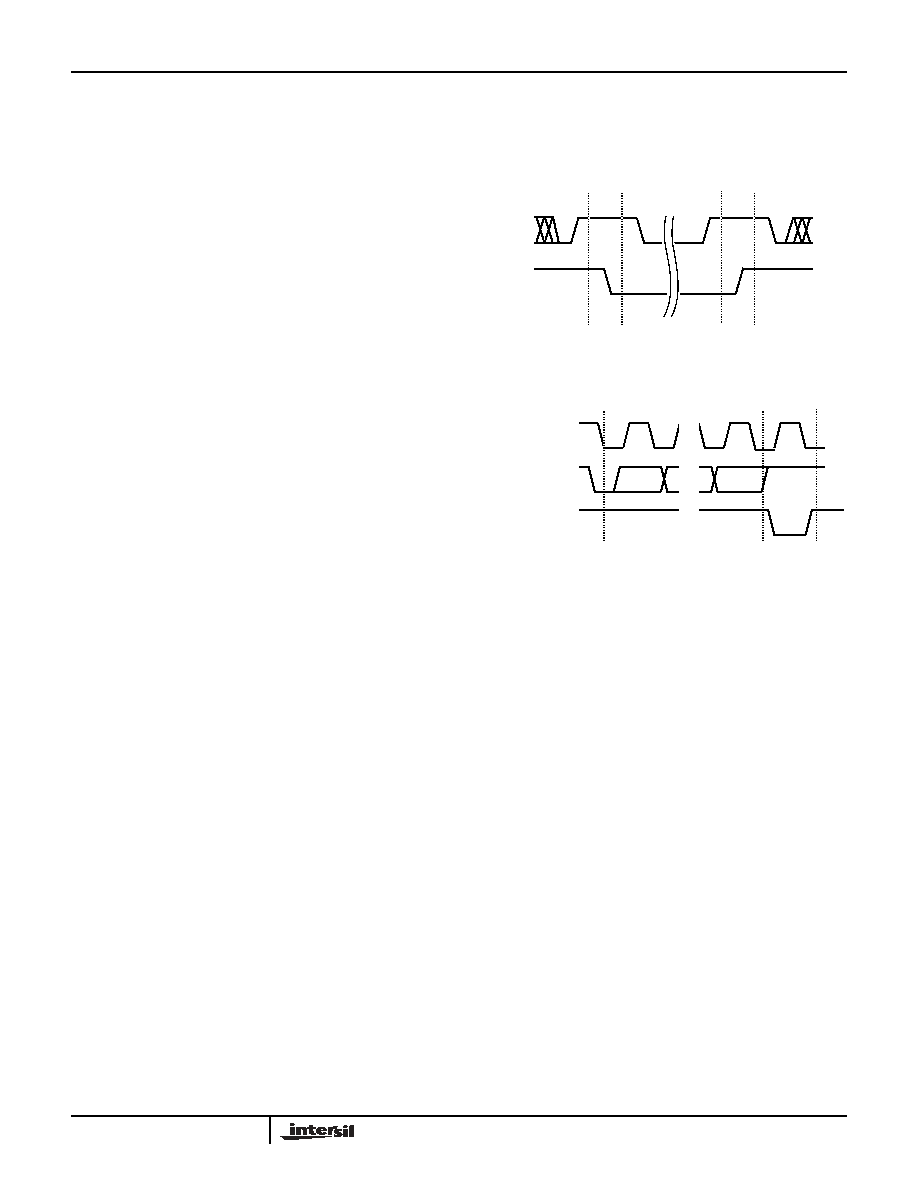
32
FN8148.0
March 18, 2005
Bus Interface Information
Interface Conventions
The device supports a bidirectional bus oriented protocol.
The protocol defines any device that sends data onto the
bus as a transmitter, and the receiving device as the
receiver. The device controlling the transfer is called the
master and the device being controlled is called the slave.
The master always initiates data transfers, and provides the
clock for both transmit and receive operations. Therefore,
the devices in this family operate as slaves in all
applications.
It should be noted that the ninth clock cycle of the read
operation is not a "don't care." To terminate a read operation,
the master must either issue a stop condition during the
ninth cycle or hold SDA HIGH during the ninth clock cycle
and then issue a stop condition.
Serial Clock and Data
Data states on the SDA line can change only during SCL
LOW. SDA state changes during SCL HIGH are reserved for
indicating start and stop conditions (See Figure 37).
Serial Start Condition
All commands are preceded by the start condition, which is a
HIGH to LOW transition of SDA when SCL is HIGH. The
device continuously monitors the SDA and SCL lines for the
start condition and will not respond to any command until
this condition has been met.
Serial Stop Condition
All communications must be terminated by a stop condition,
which is a LOW to HIGH transition of SDA when SCL is
HIGH, followed by a HIGH to LOW transition of SCL. The
stop condition is also used to place the device into the
Standby power mode after a read sequence.
Serial Acknowledge
Acknowledge is a software convention used to indicate
successful data transfer. The transmitting device, either
master or slave, will release the bus after transmitting eight
bits. During the ninth clock cycle, the receiver will pull the
SDA line LOW to acknowledge that it received the eight bits
of data (See Figure 38).
The device will respond with an acknowledge after
recognition of a start condition and if the correct Device
Identifier and Select bits are contained in the Slave Address
Byte. If a write operation is selected, the device will respond
with an acknowledge after the receipt of each subsequent
eight bit word. The device will acknowledge all incoming data
and address bytes, except for the Slave Address Byte when
the Device Identifier and/or Select bits are incorrect.
In the read mode, the device will transmit eight bits of data,
release the SDA line, then monitor the line for an
acknowledge. If an acknowledge is detected and no stop
condition is generated by the master, the device will continue
to transmit data. The device will terminate further data
transmissions if an acknowledge is not detected. The master
must then issue a stop condition to return the device to
Standby mode and place the device into a known state.
Device Addressing
Addressing Protocol Overview
Depending upon the operation to be performed on each of
these individual parts, a 1, 2 or 3 Byte protocol is used. All
operations however must begin with the Slave Address Byte
being clocked into the SMBus port on the SCL and SDA
pins. The Slave address selects the part of the device to be
addressed, and specifies if a Read or Write operation is to
be performed.
Slave Address Byte
Following a START condition, the master must output a
Slave Address Byte. This byte consists of three parts:
∑ The Device Type Identifier which consists of the most
significant four bits of the Slave Address (SA7 - SA4). The
SCL
SDA
Start
Stop
FIGURE 37. VALID START AND STOP CONDITIONS
Data Output from
Transmitter
Data Output from
Receiver
8
1
9
Start
Acknowledge
SCL from
Master
FIGURE 38. ACKNOWLEDGE RESPONSE FROM RECEIVER
X80000, X80001

33
FN8148.0
March 18, 2005
Device Type Identifier MUST be set to 1010 in order to
select the device.
∑ The next two bits (SA3 - SA2) are slave address bits. The
bits received via the SMBus are compared to A0 and A1
pins and must match or the communication is aborted.
∑ The next bit, SA1, selects the device memory sector.
There are two addressable sectors: the memory array and
the control, fault detection and remote shutdown registers.
∑ The Least Significant Bit of the Slave Address (SA0) Byte
is the R/W bit. This bit defines the operation to be
performed. When the R/W bit is "1", then a READ
operation is selected. A "0" selects a WRITE operation
(Refer to Figure 39).
Serial Write Operations
In order to perform a write operation to either a Control
Register or the EEPROM array, the Write Enable Latch
(WEL) bit must first be set.
Writes to the WEL bit do not cause a high voltage write
cycle, so the device is ready for the next operation
immediately after the stop condition.
Byte Write
For a write operation, the device requires the Slave Address
Byte and a Word Address Byte. This gives the master
access to any one of the words in the array. After receipt of
the Word Address Byte, the device responds with an
acknowledge, and awaits the next eight bits of data. After
receiving the 8 bits of the Data Byte, the device again
responds with an acknowledge. The master then terminates
the transfer by generating a stop condition, at which time the
device begins the internal write cycle to the nonvolatile
memory. During this internal write cycle, the device inputs
are disabled, so the device will not respond to any requests
from the master. The SDA output is at high impedance.
A write to a protected block of memory will suppress the
acknowledge bit.
Page Write
The device is capable of a page write operation (See Figure
40). It is initiated in the same manner as the byte write
operation; but instead of terminating the write cycle after the
first data byte is transferred, the master can transmit an
unlimited number of 8-bit bytes. After the receipt of each
byte, the device will respond with an acknowledge, and the
address is internally incremented by one. The page address
remains constant. When the counter reaches the end of the
page, it "rolls over" and goes back to `0' on the same page
(See Figure 41).
This means that the master can write 16 bytes to the page
starting at any location on that page. If the master begins
writing at location 10, and loads 12 bytes, then the first 6
bytes are written to locations 10 through 15, and the last 6
bytes are written to locations 0 through 5. Afterwards, the
address counter would point to location 6 of the page that
was just written. If the master supplies more than 16 bytes of
data, then new data overwrites the previous data, one byte
at a time.
The master terminates the Data Byte loading by issuing a
stop condition, which causes the device to begin the
nonvolatile write cycle. As with the byte write operation, all
inputs are disabled until completion of the internal write
cycle.
Stop and Write Modes
Stop conditions that terminate write operations must be sent
by the master after sending at least 1 full data byte plus the
subsequent ACK signal. If a stop is issued in the middle of a
data byte, or before 1 full data byte plus its associated ACK
is sent, then the device will reset itself without performing the
write. The contents of the array will not be effected.
Acknowledge Polling
The disabling of the inputs during high voltage cycles can be
used to take advantage of the typical 5ms write cycle time.
Once the stop condition is issued to indicate the end of the
master's byte load operation, the device initiates the internal
high voltage cycle. Acknowledge polling can be initiated
immediately. To do this, the master issues a start condition
followed by the Slave Address Byte for a write or read
operation. If the device is still busy with the high voltage
cycle then no ACK will be returned. If the device has
completed the write operation, an ACK will be returned and
the host can then proceed with the read or write operation
(See Figure 44).
SA6
SA7
SA5
SA3
SA2
SA1
SA0
DEVICE TYPE
IDENTIFIER
READ /
SA4
R/W
1
0
1
0
WRITE
ADDRESS
EXTERNAL
DEVICE
Memory
Select
A1
A0
MS
INTERNAL
ADDRESS (SA1)
INTERNALLY ADDRESSED
DEVICE
0
EEPROM Array
1
Control Register,
Fault Detection Register,
Remote Shutdown Register
BIT SA0
OPERATION
0
WRITE
1
READ
FIGURE 39. SLAVE ADDRESS FORMAT
X80000, X80001
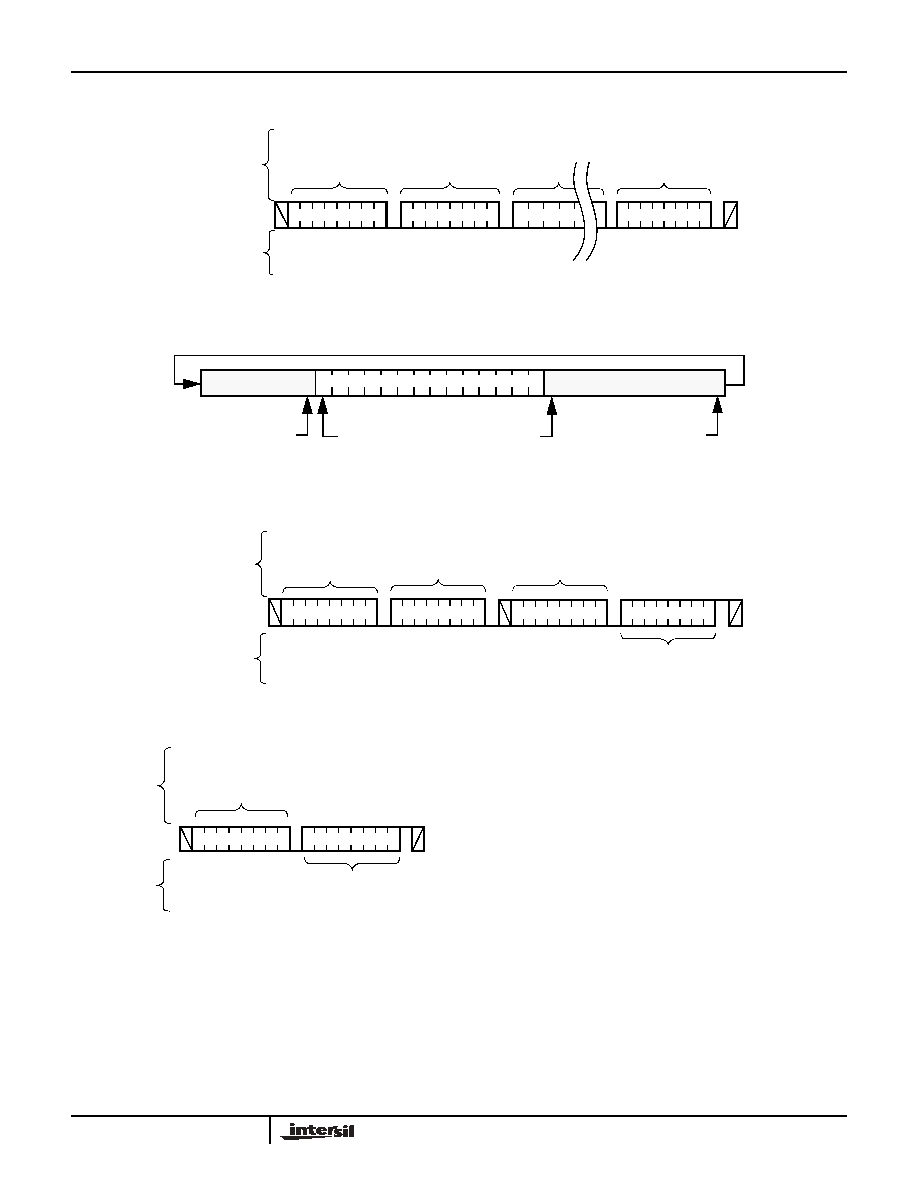
34
FN8148.0
March 18, 2005
S
t
a
r
t
S
t
o
p
Slave
Address
Byte
Address
Data
(n)
A
C
K
A
C
K
A
C
K
SDA Bus
Signals from
the Slave
Signals from
the Master
0
Data
(1)
A
C
K
(1 to n to 16)
1 0 1 0
FIGURE 40. PAGE WRITE OPERATION
address
address
10
5 Bytes
n-1
7 Bytes
address
= 6
address pointer
ends here
Addr = 7
FIGURE 41. WRITING 12 BYTES TO A 16-BYTE PAGE STARTING AT LOCATION 10
0
Slave
Address
Byte
Address
A
C
K
A
C
K
S
t
a
r
t
S
t
o
p
Slave
Address
Data
A
C
K
1
S
t
a
r
t
SDA Bus
Signals from
the Slave
Signals from
the Master
1 0 1 0
1 0 1 0
FIGURE 42. RANDOM ADDRESS READ SEQUENCE
S
t
a
r
t
S
t
o
p
Slave Address
Data
SDA Bus
Signals from
the Slave
Signals from
the Master
1
A
C
K
1 0 1 0
FIGURE 43. CURRENT ADDRESS READ SEQUENCE
X80000, X80001

35
FN8148.0
March 18, 2005
Serial Read Operations
Read operations are initiated in the same manner as write
operations with the exception that the R/W bit of the Slave
Address Byte is set to one. There are three basic read
operations: Current Address Reads, Random Reads, and
Sequential Reads.
Random Read
Random read operation allows the master to access any
memory location in the array. Prior to issuing the Slave
Address Byte with the R/W bit set to one, the master must
first perform a "dummy" write operation. The master issues
the start condition and the Slave Address Byte, receives an
acknowledge, then issues the Word Address Bytes. After
acknowledging receipts of the Word Address Bytes, the
master immediately issues another start condition and the
Slave Address Byte with the R/W bit set to one. This is
followed by an acknowledge from the device and then by the
eight bit word. The master terminates the read operation by
not responding with an acknowledge and then issuing a stop
condition. See Figure 42 for the address, acknowledge, and
data transfer sequence.
Current Address Read
Internally the device contains an address counter that
maintains the address of the last word read incremented by
one. Therefore, if the last read was to address n, the next
read operation would access data from address n+1. On
power up, the address of the address counter is undefined,
requiring a read or write operation for initialization.
Upon receipt of the Slave Address Byte with the R/W bit set
to one, the device issues an acknowledge and then
transmits the eight bits of the Data Byte. The master
terminates the read operation when it does not respond with
an acknowledge during the ninth clock and then issues a
stop condition. See Figure 43 or the address, acknowledge,
and data transfer sequence.
Operational Notes
The device powers-up in the following state:
∑ The device is in the low power standby state.
∑ The WEL bit is set to `0'. In this state, it is not possible to
write to the device.
∑ SDA pin is the input mode.
Data Protection
The following circuitry has been included to prevent
inadvertent writes:
∑ The WEL bit must be set to allow write operations.
∑ The proper clock count and bit sequence is required prior
to the stop bit in order to start a nonvolatile write cycle.
ACK
Returned?
Issue Slave Address
Byte (Read or Write)
Byte Load Completed by
Issuing STOP.
Enter ACK Polling
Issue STOP
Issue START
NO
YES
High Voltage Cycle
Complete. Continue
Command Sequence?
Issue STOP
NO
Continue Normal Read
or Write Command
Sequence
PROCEED
YES
FIGURE 44. ACKNOWLEDGE POLLING SEQUENCE
X80000, X80001

36
FN8148.0
March 18, 2005
Packaging Information
0.009 (0.23)
0.015 (0.38)
0.185
(4.70)
0.025 (0.65) BSC
0.014 (0.35)
0.029 (0.75)
(4.70)
0.185
(4.70)
0.027 (0.70)
0.031 (0.80)
0.000 (0.00)
0.030 (0.76)
0.007 (0.19)
0.009 (0.25)
0.000 (0.00)
0.002 (0.05)
0.271 (6.90)
0.279 (7.10)
0.271 (6.90)
0.279 (7.10)
PIN 1 INDENT
32-Lead Very Very Thin Quad Flat No Lead Package
7mm x 7mm Body with 0.65mm Lead Pitch
X80000, X80001

37
All Intersil U.S. products are manufactured, assembled and tested utilizing ISO9000 quality systems.
Intersil Corporation's quality certifications can be viewed at www.intersil.com/design/quality
Intersil products are sold by description only. Intersil Corporation reserves the right to make changes in circuit design, software and/or specifications at any time without
notice. Accordingly, the reader is cautioned to verify that data sheets are current before placing orders. Information furnished by Intersil is believed to be accurate and
reliable. However, no responsibility is assumed by Intersil or its subsidiaries for its use; nor for any infringements of patents or other rights of third parties which may result
from its use. No license is granted by implication or otherwise under any patent or patent rights of Intersil or its subsidiaries.
For information regarding Intersil Corporation and its products, see www.intersil.com
FN8148.0
March 18, 2005
X80000, X80001