
1
Æ
FN8149.0
CAUTION: These devices are sensitive to electrostatic discharge; follow proper IC Handling Procedures.
1-888-INTERSIL or 321-724-7143
|
Intersil (and design) is a registered trademark of Intersil Americas Inc.
Copyright Intersil Americas Inc. 2005. All Rights Reserved
All other trademarks mentioned are the property of their respective owners.
PRELIMINARY
X80010, X80011, X80012, X80013
Penta-Power Sequence Controller
with Hot swap and System Management
The X80010, X80011, X80012, X80013 contain three major
functions: a power sequencing controller, a hotswap
controller, and systems management support.
The power sequencer controller time sequences up to five
DC/DC modules. The device allows various DC/DC power
sequencing configurations, either parallel or relay modes.
The power good, enable, and voltage good signals provide
for flexible DC/DC timing configurations. Each voltage
enable signal has a built-in delay while additional delay can
be added with simple external passive components.
The hot swap controller allows a board to be safely inserted
and removed from a live backplane without turning off the
main power supply. The X80010 family of devices offers a
modular, power distribution approach by providing flexibility
to solve the hotswap and power sequencing issues for
insertion, operations, and extraction. Hardshort Detection
and Retry with Delay, Noise filtering, Insertion Overcurrent
Bypass, and Gate Current selection are some of the
integrated features of the device. During insertion, the gate
of an external power MOSFET is clamped low to suppress
contact bounce. The undervoltage/overvoltage circuits and
the power on reset circuitry suppress the gate turn on until
the mechanical bounce has ended. The X80010 turns on the
gate with a user set slew rate to limit the inrush current and
incorporates an electronic circuit breaker set by a sense
resistor. After the load is successfully charged, the PWRGD
signal is asserted; indicating that the device is ready to
power sequence the DC/DC power bricks.
Systems management function provides a reset signal
indicating that the power good and all the voltage good
signals are active. The reset signal is asserted after a wait
state delay. This signal is used to coordinate the hotswap
and DC/DC module latencies during power up to avoid
"power hang up". In addition, the CPU host can initiate soft
insertion or DC voltage module re-sequencing.
Features
∑ Integrates Three Major Functions
- Power Sequencing
- Hot Swap Controller
- System Management Functions
∑ Penta-Power Sequencing
- Sequence up to 5 DC/DC converters.
- Four independent voltage enable pins
- Four time delay circuits
- Soft Power Sequencing - MRC pin restarts sequence
without power cycling.
∑ Hot Swap Controller
- Programmable overvoltage and undervoltage protection
- Undervoltage lockout for battery/redundant supplies
- Electronic circuit breaker - Overcurrent Detection and
Gate Shut-off
- Overcurrent limit during Insertion
- Hardshort retry with retry failure flag
- Selectable gate current using IGQ pins (10, 70, 150µA)
- MRH pin controls board insertion/extraction.
- Typically operates from -30V to -80V. Tolerates
transients to -200V (limited by external components)
∑ System Management
- Reset output, with delay, holds off host until all supplies
are good
- Host control of reinsertion with MRH input
- Host control of resequencing using MRC input
∑ Available packages
- 32-lead Quad No-Lead Frame (QFN)
Applications
∑ -48V Hot Swap Power Backplane/Distribution Central
Office, Ethernet for VOIP
∑ Card Insertion Detection
∑ Power Sequencing DC/DC/Power Bricks
∑ IP Phone Applications
∑ Databus Power Interfacing
∑ Custom Industrial Power Backplanes
∑ Distributed Power Systems
Data Sheet
January 13, 2005

2
FN8149.0
January 13, 2005
Pinout
Typical Application
V1GOOD
MRC
NA1
V3GOOD
V2GOOD
EN4
EN3
EN1
RESET
NA1
V4GOOD
DRAI
N
PW
R
G
D
SE
NS
E
V
UV/O
V
I
GQ
0
V
EE
GA
TE
V
DD
FA
R
BA
T
T
-
O
N
MRH
I
GQ
1
NA2
1
2
3
4
5
6
7
9 10 11 12 13 14
18
19
20
21
22
23
24
26
27
28
29
30
31
32
NA2
EN2
8
17
NA1
V
EE
15
25
V
RGO
16
NA1
NC
NC
QFN package
(Top view)
(7mm x 7mm)
Ordering Information
ORDER
NUMBER
OV
(V)
UV1
(V)
UV2
(V)
t
NF
(us)
V
OC
(mV)
V
OCI
(mV)
OVER
CURRENT
RETRY
RETRY
DELAY
(ms)
I
GATE
(µA)
T
DELAY
(ms)
t
POR
(ms)
TEMP RANGE
(∞C)
PART
MARK
X80010Q32I
74.9
42.4
33.2
5
50
150
Always
100
50
100
100
-40 to 85
80010I
X80011Q32I
68.0
42.4
33.2
5
50
150
Always
100
50
100
100
-40 to 85
80011I
X80012Q32I
74.9
42.4
33.2
5
50
150
5 retries
100
50
100
100
-40 to 85
80012I
X80013Q32I
68.0
42.4
33.2
5
50
150
5 retries
100
50
100
100
-40 to 85
80013I
V
DD
X80010, X80011,
V
UV/OV
V
EE
SENSE
DRAIN
-48V
UV=37V
OV=71V
-48V
GATE
Rs
0.02
5%
R4
182k
1%
R5
30k
1%
R6
10k
1%
Q1
IRFR120
RTN
V1GOOD
V2GOOD
V3GOOD
DC/DC
Module
1
ON/OFF
DC/DC
Module
2
ON/OFF
DC/DC
Module
3
ON/OFF
DC/DC
Module
4
ON/OFF
PWRGD
EN1
EN2
EN3
4.7V
12V
V1
V2
V3
V4
100
0.1uF
Back-
Plane
100K
4.7K
3.3n
X80012, X80013
X80010, X80011, X80012, X80013
3
FN8149.0
January 13, 2005
Absolute Maximum Ratings
Recommended Operating Conditions
Temperature under bias . . . . . . . . . . . . . . . . . . . . . ≠65∞C to +135∞C
Storage temperature . . . . . . . . . . . . . . . . . . . . . . . ≠65∞C to +150∞C
Voltage on given pin (Hot Side Functions):
V
ov/uv pin
. . . . . . . . . . . . . . . . . . . . . . . . . . . . . . . . . . . . .5.5V + V
EE
SENSE pin . . . . . . . . . . . . . . . . . . . . . . . . . . . . . . . . . .400mV + V
EE
V
EE
pin . . . . . . . . . . . . . . . . . . . . . . . . . . . . . . . . . . . . . . . . . . . -80V
DRAIN pin . . . . . . . . . . . . . . . . . . . . . . . . . . . . . . . . . . . . 48V + V
EE
PWRGD pin . . . . . . . . . . . . . . . . . . . . . . . . . . . . . . . . . . . . 7V + V
EE
GATE pin . . . . . . . . . . . . . . . . . . . . . . . . . . . . . . . . . . . . . V
DD
+ V
EE
FAR pin . . . . . . . . . . . . . . . . . . . . . . . . . . . . . . . . . . . . . . . 7V + V
EE
MRH pin . . . . . . . . . . . . . . . . . . . . . . . . . . . . . . . . . . . . . .5.5V + V
EE
BATT_ON pin. . . . . . . . . . . . . . . . . . . . . . . . . . . . . . . . . .5.5V + V
EE
Voltage on given pin (Cold Side Functions):
ENi pins (i = 1 to 4) . . . . . . . . . . . . . . . . . . . . . . . . . . . . . . . . . . . .5V
ViGOOD pins (i = 1 to 4) . . . . . . . . . . . . . . . . . . . . . . . . .5.5V + V
EE
RESET pin . . . . . . . . . . . . . . . . . . . . . . . . . . . . . . . . . . . .5.5V + V
EE
MRC pin . . . . . . . . . . . . . . . . . . . . . . . . . . . . . . . . . . . . . .5.5V + V
EE
IGQ1 and IGQ0 pins . . . . . . . . . . . . . . . . . . . . . . . . . . . .5.5V + V
EE
V
DD
pin . . . . . . . . . . . . . . . . . . . . . . . . . . . . . . . . . . . . . . 14V + V
EE
D.C. output current. . . . . . . . . . . . . . . . . . . . . . . . . . . . . . . . . . . 5mA
Lead temperature (soldering, 10 seconds) . . . . . . . . . . . . . . . 300∞C
Temperature Range (Industrial) . . . . . . . . . . . . . . . . . . -40∞C to 85∞C
Supply Voltage (V
DD
) . . . . . . . . . . . . . . . . . . . . . . . . . . . . . . . . .12V
CAUTION: Stresses above those listed under "Absolute Maximum Ratings" may cause permanent damage to the device. This is a stress rating only; functional
operation of the device (at these or any other conditions above those listed in the operational sections of this specification) is not implied. Exposure to absolute maximum
rating conditions for extended periods may affect device reliability.
Electrical Specifications
(Standard Settings)
Over the recommended operating conditions unless otherwise specified.
SYMBOL
PARAMETER
TEST CONDITIONS
MIN
TYP
MAX
UNIT
DC CHARACTERISTICS
V
DD
Supply Operating Range
10
12
14
V
I
DD
Supply Current
2.5
5
mA
V
RGO
Regulated 5V output
I
RGO
= 10µA
4.5
6.0
I
RGO
V
RGO
current output
50
µA
I
GATE
Gate Pin Current
Gate Drive On,
V
GATE
= V
EE
,
V
SENSE
= V
EE
(sourcing)
46.2
52.5
58.8
µA
V
GATE
- V
EE
= 3V
V
SENSE
-V
EE
= 0.1V (sinking)
9
mA
V
GATE
External Gate Drive (Slew Rate Control)
I
GATE
= 50µA
V
DD
-1
V
DD
V
V
PGA
Power Good Threshold
(PWRGD High to Low)
Referenced to V
EE
V
UV1
< V
UV/OV
< V
OV
0.9
1
1.1
V
V
IHB
Voltage Input High (BATT_ON)
V
EE
+ 4
V
EE
+ 5
V
V
ILB
Voltage Input Low (BATT_ON)
V
EE
+ 2
V
I
LI
Input Leakage Current (MRH, MRC)
V
IL
= GND to V
CC
10
µA
I
LO
Output Leakage Current
(V1GOOD, V2GOOD, V3GOOD, V4GOOD,
RESET)
All ENi = V
RGO
for i = 1 to 4
10
µA
V
IL
(3)
Input LOW Voltage (MRH, MRC, IGQ0, IGQ1)
-0.5 + V
EE
(V
EE
+ 5) x
0.3
V
V
IH
(3)
Input HIGH Voltage (MRH, MRC, IGQ0, IGQ1)
(V
EE
+ 5)
x
0.7
(V
EE
+ 5) +
0.5
V
X80010, X80011, X80012, X80013
4
FN8149.0
January 13, 2005
V
OL
Output LOW Voltage
(RESET, RESET, V1GOOD, V2GOOD,
V3GOOD, V4GOOD, FAR, PWRGD)
I
OL
= 4.0mA
(V
EE
+ 2.7 to V
EE
+ 5.5V)
I
OL
= 2.0mA
(V
EE
+ 2.7 to V
EE
+ 3.6V)
V
EE
+ 0.4
V
C
OUT
(1)
Output Capacitance
(RESET, V1GOOD, V2GOOD, V3GOOD,
V4GOOD, FAR)
V
OUT
= 0V
8
pF
C
IN
(1)
Input Capacitance (MRH, MRC)
V
IN
= 0V
6
pF
V
OC
Over-current threshold
V
OC
= V
SENSE
- V
EE
45
50
55
mV
V
OCI
Over-current threshold (Insertion)
V
OC
= V
SENSE
- V
EE
PWRGD = HIGH
Initial Power Up condition
135
150
165
mV
V
OVR
Overvoltage threshold (rising)
X80010, X80012
X80011, X80013
Referenced to V
EE
3.85
3.49
3.90
3.54
3.95
3.59
V
V
OVH
Overvoltage hysteresis
Referenced to V
EE
12
18
24
mV
V
UV1H
Undervoltage 1 hysteresis
Referenced to V
EE
BATT-ON = V
EE
12
18
24
mV
V
UV1F
Undervoltage 1 threshold (falling)
2.16
2.21
2.26
V
V
UV2H
Undervoltage 2 hysteresis
Referenced to V
EE
BATT-ON = V
RGO
12
18
24
mV
V
UV2F
Undervoltage 2 threshold (falling)
1.68
1.73
1.78
V
V
DRAINF
Drain sense voltage threshold
(falling)
Referenced to V
EE
0.9
1
1.1
V
V
DRAINR
Drain sense voltage threshold
(rising)
Referenced to V
EE
1.2
1.3
1.4
V
V
TRIP1
EN1 Trip Point Voltage
Referenced to V
EE
2.25
2.5
2.75
V
V
TRIP2
EN2 Trip Point Voltage
Referenced to V
EE
2.25
2.5
2.75
V
V
TRIP3
EN3 Trip Point Voltage
Referenced to V
EE
2.25
2.5
2.75
V
V
TRIP4
EN4 Trip Point Voltage
Referenced to V
EE
2.25
2.5
2.75
V
AC CHARACTERISTICS
t
FOC
Sense High to Gate Low
1.5
2.5
3.5
µs
t
FUV
Under Voltage conditions to Gate Low
0.5
1.0
1.5
µs
t
FOV
Overvoltage Conditions to Gate Low
1.0
1.5
2
µs
t
VFR
Overvoltage/undervoltage failure recovery time
to Gate =1V.
V
DD
does not drop below 3V, No
other failure conditions.
1.2
1.6
2
µs
t
BATT_ON
Delay BATT_ON Valid
100
ns
t
MRC
Minimum time high for reset valid on the MRC
pin
5
µs
t
MRH
Minimum time high for reset valid on the MRH
pin
5
µs
t
MRCE
Delay from MRC enable to PWRGD HIGH
No Load
1.0
1.6
µs
t
MRCD
Delay from MRC disable to PWRGD LOW
Gate is On, No Load
200
400
µs
t
MRHE
Delay from MRH enable to Gate Pin LOW
I
GATE
= 60µA, No Load
1.0
1.6
2.4
µs
t
MRHD
Delay from MRH disable to GATE reaching 1V I
GATE
= 60µA, No Load
1.8
2.6
µs
Electrical Specifications
(Standard Settings)
Over the recommended operating conditions unless otherwise specified. (Continued)
SYMBOL
PARAMETER
TEST CONDITIONS
MIN
TYP
MAX
UNIT
X80010, X80011, X80012, X80013
5
FN8149.0
January 13, 2005
Equivalent A.C. Output Load Circuit
t
RESET_E
Delay from PWRGD or ViGOOD to RESET
valid LOW
1
µs
t
QC
Delay from IGQ1 and IGQ0 to valid Gate pin
current
1
µs
t
SC_RETRY
Delay between Retries
85
100
115
ms
t
NF
Noise Filter for Overcurrent
4.5
5
5.5
µs
t
DPOR
Device Delay before Gate assertion
45
50
55
ms
t
SPOR
Delay after PWRGD and all ViGOOD signals
are active before RESET assertion
85
100
115
ms
t
DELAY1
Power Sequencing Time Delay
T
i
D1 = 0; T
i
D0 = 0
85
100
115
ms
t
DELAY2
t
DELAY3
t
DELAY4
t
TO
ViGOOD turn off time
50
ns
t
PDHLPG
(1)
Delay from Drain good to PWRGD LOW
Gate = V
DD
1
µs
t
PDLHPG
(1)
Delay from Drain fail to PWRGD HIGH
Gate = V
DD
1
µs
t
PGHLPG
(1)
Delay from Gate good to PWRGD LOW
Drain = V
EE
1
µs
t
PGLHPG
(1)
Delay from Gate fail to PWRGD HIGH
Drain = V
EE
1
µs
NOTE:
1.
This parameter is based on characterization data.
Electrical Specifications
(Standard Settings)
Over the recommended operating conditions unless otherwise specified. (Continued)
SYMBOL
PARAMETER
TEST CONDITIONS
MIN
TYP
MAX
UNIT
A.C. Test Conditions
Input pulse levels
V
CC
x 0.1 to V
CC
x 0.9
Input rise and fall times
10ns
Input and output timing levels
V
CC
x 0.5
Output load
Standard output load
4.6k
RESET
30pF
V1GOOD,
5V
4.6k
30pF
V2GOOD,
V3GOOD,
V4GOOD
FAR
5V
PWRGD
X80010, X80011, X80012, X80013

6
FN8149.0
January 13, 2005
SENSE
V
UV/OV
V
OV
V
UV
V
DD
V
TH
MRH
GATE
V
OC
V
OCI
t
VFR
t
FOV
t
FUV
t
DPOR
t
VFR
1V
1V
FIGURE 1. OVERVOLTAGE/UNDERVOLTAGE GATE TIMING
SENSE
V
DD
V
TH
GATE
V
OC
V
OCI
t
DPOR
t
SC_RETRY
t
FOC
t
FOC
Always Retry
V
UV
< V
UV/OV
<
V
OV
t
SC_RETRY
MRH = HIGH
FIGURE 2. OVERCURRENT GATE TIMING
ENi
t
TO
ViGOOD
V
TRIPi
t
DELAYi
i = 1, 2, 3, 4
Initial
Power-up
t
TO
V
DD
Enable DC/DC supply
FIGURE 3. ViGOOD TIMINGS
X80010, X80011, X80012, X80013

7
FN8149.0
January 13, 2005
t
MRHD
GATE
t
MRHE
MRH
t
MRH
1V
FIGURE 4. MANUAL RESET (HOT SIDE) MRH
t
MRCD
PWRGD
MRC
t
MRCE
t
MRC
FIGURE 5. MANUAL RESET (COLD SIDE) MRC
PWRGD
t
DELAY1
V1GOOD
t
DELAY2
V2GOOD
t
DELAY3
V3GOOD
t
DELAY4
V4GOOD
t
SPOR
RESET
t
RESET_E
PWRGD or
V
DRAIN
t
GLHPG
t
GHLPG
V
GATE
t
DLHPG
t
DHLPG
ENi
any ENi LOW to HIGH
(1st occurance)
FIGURE 6. RESET TIMINGS
X80010, X80011, X80012, X80013
8
FN8149.0
January 13, 2005
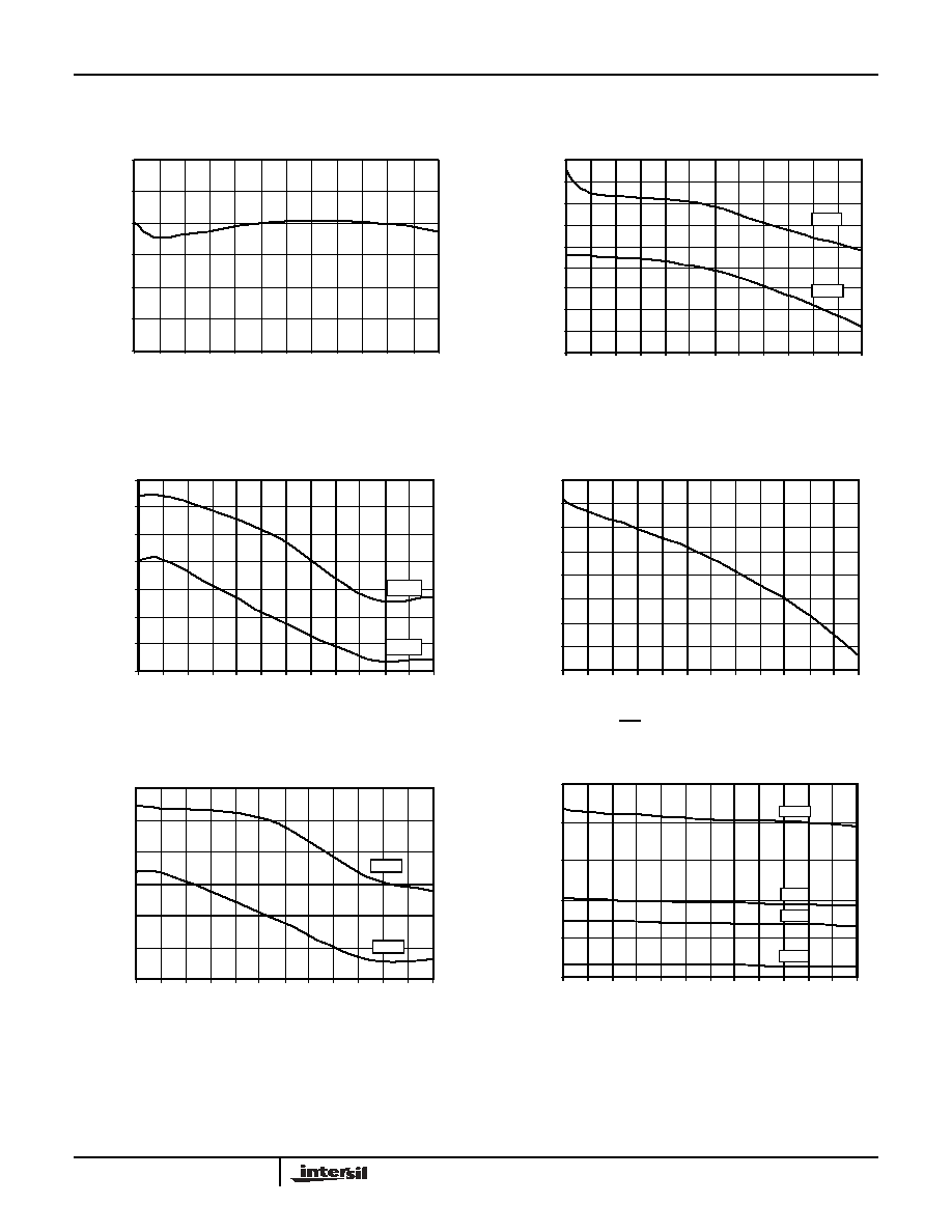
Typical Performance Characteristics
FIGURE 7. OVER CURRENT THRESHOLD vs
TEMPERATURE
FIGURE 8. UNDERVOLTAGE 2 THRESHOLD vs
TEMPERATURE
FIGURE 9. OVERVOLTAGE THRESHOLD vs TEMPERATURE
FIGURE 10. ENi THRESHOLD vs TEMPERATURE
FIGURE 11. UNDERVOLTAGE 1 THRESHOLD vs
TEMPERATURE
FIGURE 12. I
GATE
(SOURCE) vs TEMPERATURE
46.000
47.000
48.000
49.000
50.000
51.000
52.000
-55
-40 -25 -10
5
20
35
50
65
80
95
110 125
TEMPERATURE
INRUSH CURRENT
LIMIT (m
V
)
1.690
1.700
1.710
1.720
1.730
1.740
1.750
1.760
1.770
1.780
-55
-40 -25 -10
5
20
35
50
65
80
95
110 125
TEMPERATURE
Rising
Falling
UNDER VOLTAGE
2 THRESHOL
D (V)
3.85
3.86
3.87
3.88
3.89
3.90
3.91
3.92
-55 -40 -25 -10
5
20
35
50
65
80
95 110 125
TEMPERATURE
Rising
Falling
OV THRESHOL
D (V)
2.475
2.480
2.485
2.490
2.495
2.500
2.505
2.510
2.515
-55 -40 -25 -10
5
20
35
50
65
80
95 110 125
TEMPERATURE
ENi THRESHO
L
D (V)
2.190
2.200
2.210
2.220
2.230
2.240
2.250
-55
-40 -25 -10
5
20
35
50
65
80
95 110 125
TEMPERATURE
Rising
Falling
UND
E
R
V
O
LTAGE 1 TH
RE
SHOLD (V)
0
40
80
120
160
200
-55 -40 -25 -10
5
20
35
50
65
80
95 110 125
TEMPERATURE
150µA
70µA
50µA
10µA
GATE CURRENT
(µA)
X80010, X80011, X80012, X80013

9
FN8149.0
January 13, 2005
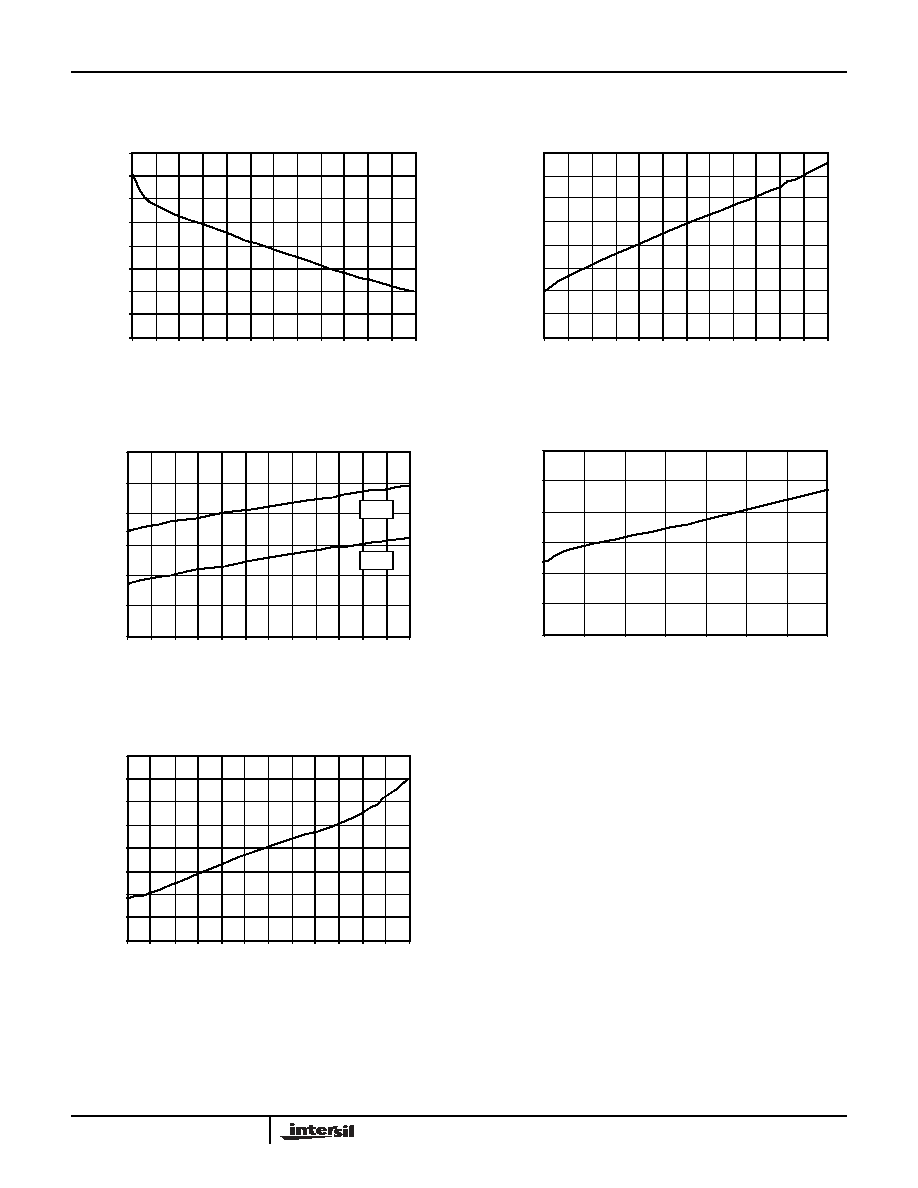
FIGURE 13. I
GATE
(SINK) vs TEMPERATURE
FIGURE 14. T
FOC
vs TEMPERATURE
FIGURE 15. t
FUV
vs TEMPERATURE
FIGURE 16. t
DELAYi
vs TEMPERATURE
FIGURE 17. t
FOV
vs TEMPERATURE
Typical Performance Characteristics
(Continued)
7.0
7.5
8.0
8.5
9.0
9.5
10.0
10.5
11.0
-55 -40 -25 -10
5
20
35
50
65
80
95 110 125
TEMPERATURE
GATE CU
RRE
N
T
- SINK
(mA)
1.7
1.8
1.9
2.0
2.1
2.2
2.3
2.4
2.5
-55 -40 -25 -10
5
20
35
50
65
80
95 110 125
TEMPERATURE
t
OC
(µs)
0.500
0.550
0.600
0.650
0.700
0.750
0.800
-55
-40 -25 -10
5
20
35
50
65
80
95 110 125
TEMPERATURE
tUV1
tUV2
t
UV
(µs)
0.90
0.92
0.94
0.96
0.98
1.00
1.02
-55
-35
-15
5
25
45
65
85
TEMPERATURE
t
DELA
Y
(N
OR
M
A
L
I
Z
E
D
)
1.0
1.1
1.1
1.2
1.2
1.3
1.3
1.4
1.4
-55 -40
-25 -10
5
20
35
50
65
80
95 110 125
TEMPERATURE
t
OV
(µs)
X80010, X80011, X80012, X80013
10
FN8149.0
January 13, 2005
FIGURE 18. OVER CURRENT THRESHOLD vs TEMPERATURE
FIGURE 19. UNDERVOLTAGE 2 THRESHOLD vs
TEMPERATURE
FIGURE 20. OVERVOLTAGE THRESHOLD vs TEMPERATURE
FIGURE 21. ENi THRESHOLD vs TEMPERATURE
FIGURE 22. UNDERVOLTAGE 1 THRESHOLD vs
TEMPERATURE
FIGURE 23. I
GATE
(SOURCE) vs TEMPERATURE
Typical Performance Characteristics
(Continued)
46.000
47.000
48.000
49.000
50.000
51.000
52.000
-55
-40 -25 -10
5
20
35
50
65
80
95
110 125
TEMPERATURE
INRUSH CUR
RE
NT
LIMIT (m
V
)
1.690
1.700
1.710
1.720
1.730
1.740
1.750
1.760
1.770
1.780
-55
-40 -25 -10
5
20
35
50
65
80
95
110 125
TEMPERATURE
Rising
Falling
UNDER VOLTAGE
2 THRESHOL
D (V
)
3.85
3.86
3.87
3.88
3.89
3.90
3.91
3.92
-55 -40 -25 -10
5
20
35
50
65
80
95 110 125
TEMPERATURE
Rising
Falling
OV
T
HRESHO
L
D
(V
)
2.475
2.480
2.485
2.490
2.495
2.500
2.505
2.510
2.515
-55 -40 -25 -10
5
20
35
50
65
80
95 110 125
TEMPERATURE
ENi THRES
H
OLD (
V
)
2.190
2.200
2.210
2.220
2.230
2.240
2.250
-55
-40 -25 -10
5
20
35
50
65
80
95 110 125
TEMPERATURE
Rising
Falling
UNDER
V
O
LTAGE 1 THR
E
SHOLD (V)
0
40
80
120
160
200
-55 -40 -25 -10
5
20
35
50
65
80
95 110 125
TEMPERATURE
150µA
70µA
50µA
10µA
GATE C
URRENT (µA)
X80010, X80011, X80012, X80013
11
FN8149.0
January 13, 2005
FIGURE 24. I
GATE
(SINK) vs TEMPERATURE
FIGURE 25. t
FOC
vs TEMPERATURE
FIGURE 26. t
FUV
vs TEMPERATURE
FIGURE 27. t
DELAYi
vs TEMPERATURE
FIGURE 28. t
FOV
vs TEMPERATURE
Typical Performance Characteristics
(Continued)
7.0
7.5
8.0
8.5
9.0
9.5
10.0
10.5
11.0
-55 -40 -25 -10
5
20
35
50
65
80
95 110 125
TEMPERATURE
GATE
CURRENT -
SINK (
m
A)
1.7
1.8
1.9
2.0
2.1
2.2
2.3
2.4
2.5
-55 -40 -25 -10
5
20
35
50
65
80
95 110 125
TEMPERATURE
t
OC
(µs)
0.500
0.550
0.600
0.650
0.700
0.750
0.800
-55
-40 -25 -10
5
20
35
50
65
80
95 110 125
TEMPERATURE
tUV1
tUV2
t
UV
(µ
s)
0.90
0.92
0.94
0.96
0.98
1.00
1.02
-55
-35
-15
5
25
45
65
85
TEMPERATURE
t
DELA
Y
(N
OR
M
A
L
I
Z
E
D
)
1.0
1.1
1.1
1.2
1.2
1.3
1.3
1.4
1.4
-55 -40
-25 -10
5
20
35
50
65
80
95 110 125
TEMPERATURE
t
OV
(µs)
X80010, X80011, X80012, X80013
12
FN8149.0
January 13, 2005
SENSE
V
EE
GATE
IGQ1
IGQ0
DRAIN
BATT-ON
MRC
MRH
RESET
V
DD
FAR
PWRGD
Power Good
Logic
Slew Rate
Selection
5V reg.
V
RGO
V
EE
V
EE
V
EE
V
OV
Ref
V
UV1
Ref
V
UV2
Ref
V
UV/OV
2:1
MUX
V
EE
Gate
Control
V
DD
1V Ref
V
RGO
V
OC
REF
38R
3R
Reset Logic
and Delay
V
EE
Over current
logic, Hard short
relay, Retry logic
status and delay
POR
Sequence
and Timing
Control logic
50µA
EN1
EN2
EN3
EN4
V4GOOD
V3GOOD
V2GOOD
V1GOOD
V
EE
V
EE
Divider
4
Reset
OSC
0.1s
0.5s
1s
5s
Select
4
delay1
delay2
delay3
delay4
Delay circuit
repeated 4 times
V
RGO
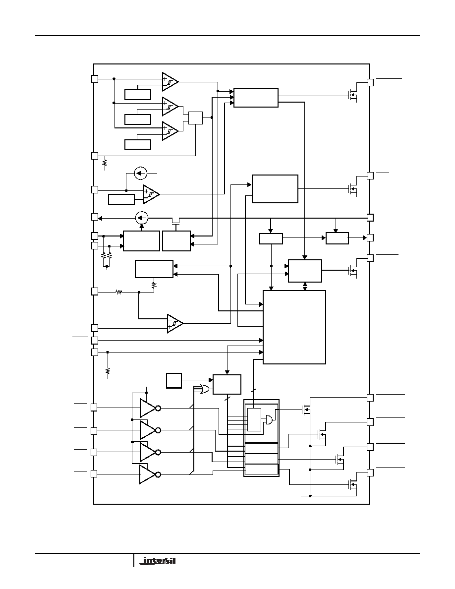
FIGURE 29. BLOCK DIAGRAM
X80010, X80011, X80012, X80013
13
FN8149.0
January 13, 2005
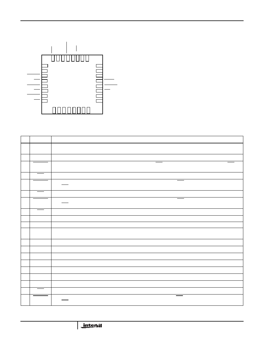
Pin Configuration
V1GOOD
MRC
NA1
V3GOOD
V2GOOD
EN4
EN3
EN1
RESET
NA1
V4GOOD
DR
AI
N
PW
RG
D
SEN
S
E
V
UV/O
V
I
GQ0
V
EE
GA
TE
V
DD
FA
R
BA
TT
-
O
N
MR
H
I
GQ
1
NA2
1
2
3
4
5
6
7
9 10 11 12 13 14
18
19
20
21
22
23
24
26
27
28
29
30
31
32
X80010, X80011, X80012, X80013
32-lead QFN Quad Package
NA2
EN2
8
17
NA
1
V
EE
15
25
V
RGO
16
NA
1
NC
NC
(7mm x 7mm)
Pin Descriptions
PIN
NAME
DESCRIPTION
1
V
RGO
Regulated 5V output. Used to pull-up
user programmable inputs IGQ0, IGQ1, BATT-ON (if needed).
2
NA1
Not Available. Do not connect to this pin.
3
V4GOOD
V4 Voltage Good Output. This open drain output goes LOW when EN4 is less than V
TRIP4
and goes HIGH when EN4 is
greater than V
TRIP4
. There is a user selectable delay circuitry on this pin.
4
EN4
V4 Voltage Enable Input. Fourth voltage enable pin. If unused connect to V
RGO
.
5
V3GOOD
V3 Voltage Good Output (Active Low). This open drain output goes LOW when EN3 is less than V
TRIP3
and goes HIGH
when EN3 is greater than V
TRIP3
. There is a user selectable delay circuitry on this pin.
6
EN3
V3 Voltage Enable Input. Third voltage enable pin. If unused connect to V
RGO
.
7
V2GOOD
V2 Voltage Good Output (Active Low). This open drain output goes LOW when EN2 is less than V
TRIP2
and goes HIGH
when EN2 is greater than V
TRIP2
. There is a user selectable delay circuitry on this pin.
8
EN2
V2 Voltage Enable Input. Second voltage enable pin. If unused connect to V
RGO
.
9
V
DD
Positive Supply Voltage Input.
10
V
EE
Negative Supply Voltage Input.
11
V
UV/OV
Analog Undervoltage and Overvoltage Input. Turns off the external N-channel MOSFET when there is an undervoltage or
overvoltage condition.
12
SENSE
Circuit Breaker Sense Input. This input pin detects the overcurrent condition.
13
GATE
Gate Drive Output. Gate drive output for the external N-channel MOSFET.
14
DRAIN
Drain. Drain sense input of the external N-channel MOSFET.
15
NA1
Not Available. Do not connect to this pin.
16
NA1
Not Available. Do not connect to this pin.
17
NA2
Not Available. Connect to V
RGO
.
18
NA2
Not Available. Connect to V
RGO
.
19
EN1
V1 Voltage Enable Input. First voltage enable pin. If unused connect to V
RGO
.
20
V1GOOD
V1 Voltage Good Output (Active Low).This open drain output goes LOW when EN1 is less than V
TRIP1
and goes HIGH
when EN1 is greater than V
TRIP1
. There is a user selectable delay circuitry on this pin.
X80010, X80011, X80012, X80013
14
FN8149.0
January 13, 2005
Functional Description
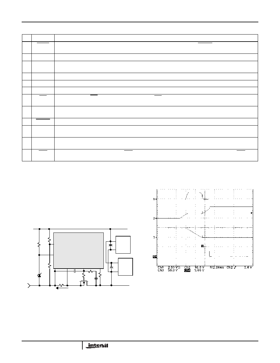
Hot Circuit Insertion
When circuit boards are inserted into a live backplane, the
bypass capacitors at the input of the board's power module
or DC/DC converter can draw huge transient currents as
they charge up (See Figure 30). This transient current can
cause permanent damage to the board's components and
cause transients on the system power supply.
The X80010 is designed to turn on a board's supply voltage
in a controlled manner (see Figure 31), allowing the board to
be safely inserted or removed from a live backplane. The
device also provides undervoltage, overvoltage and
overcurrent protection while keeping the power module
(DC/DC converter) off until the backplane input voltage is
stable and within tolerance.
Overvoltage and Undervoltage Shutdown
The X80010 provides overvoltage and undervoltage
protection circuits. When an overvoltage (V
OV
) or
undervoltage (V
UV1
and V
UV2
) condition is detected, the
GATE pin immediately pulls low. The undervoltage threshold
V
UV1
applies to the normal operation with a mains supply.
The undervoltage threshold V
UV2
assumes the system is
powered by a battery. When using a battery backup, the
21
RESET
RESET Output. This open drain pin is an active LOW output. This pin will be active until PWRGD goes active and the power
sequencing is complete. This pin will be released after a programmable delay.
22
NA1
Not Available. Do not connect to this pin.
23
MRC
Manual Reset Input Cold-side. Pulling the MRC pin HIGH initiates a system side RESET. The MRC signal must be held HIGH
for 5
µs. It has an internal pulldown resistor. (>10m typical)
24
NC
No Connect. No internal connections.
25
V
EE
Negative Supply Voltage Input.
26
NC
No Connect. No internal connections.
27
FAR
Failure After Re-try (FAR) output signal. Failure After Re-try (FAR) is asserted after a number of retries. Used for Overcurrent
and hardshort detection.
28
BATT-ON
Battery On Input. This input signals that the battery backup (or secondary supply) is supplying power to the backplane. It has
an internal pulldown resistor. (>10m
typical)
29
PWRGD
Power Good Output. This output pin enables a power module.
30
IGQ1
Gate Current Quick Select Bit 1 Input. This pin is used to change the gate current drive and is intended to allow for current
ramp rate control of the gate pin of an external FET. It has an internal pulldown resistor. (>10m
typical)
31
IGQ0
Gate Current Quick Select Bit 0 Input. This pin is used to change the gate current drive and is intended to allow for current
ramp rate control of the gate pin of an external FET. It has an internal pulldown resistor. (>10m
typical)
32
MRH
Manual Reset Input Hot-side. Pulling the MRH pin LOW initiates a GATE pin reset (GATE pin pulled LOW). The MRH signal
must be held LOW for 5
µs (minimum).
Pin Descriptions
(Continued)
PIN
NAME
DESCRIPTION
V
DD
X80010
V
UV/OV
V
EE
SENSE
DRAIN
-48V
UV=37V
OV=71V
-48V
GATE
Rs
0.02
5%
R4
182K
1%
R5
30k
1%
R6
10K
1%
Q1 IRFR120
Return
100K
-48V
DC/DC
Converter
DC/DC
Converter
I
inrush
X80011
0.1µF
100
4.7k
3.3n
X80012
X80013
FIGURE 30. TYPICAL -48V HOTSWAP APPLICATION CIRCUIT
FIGURE 31. TYPICAL INRUSH WITH GATE SLEW RATE
CONTROL
X80010, X80011, X80012, X80013

15
FN8149.0
January 13, 2005
BATT-ON pin is pulled to V
RGO
. The default thresholds have
been set so the external resistance values in Figure 30
provide an overvoltage threshold of 74.9V (X80010/X80012)
or 68V (X80011/X80013), a main undervoltage threshold of
43V and a battery undervoltage threshold of 33.8V.
As shown in Figure 34, this circuit block contains
comparators and voltage references to monitor for a single
overvoltage and dual undervoltage trip points. The
overvoltage and undervoltage trip points as shown in Table 1.
A resistor divider connected between the plus and minus
input voltages and the V
UV/OV
pin (see Figure 32)
determines the overvoltage and undervoltage shutdown
voltages and the operating voltage range. Using the
thresholds in Table and the equations of Figure 32 the
desired operating voltage can be determined. Figure 33
shows the resistance values for various operating voltages
(X80010 and X80012).
Battery Back Up Operations
An external signal, BATT_ON is provided to switch the
undervoltage trip point. The BATT_ON signal is a LOGIC
HIGH if V
IHB
> V
EE
+ 4V and is a LOGIC LOW if V
ILB
< V
EE
+ 2V. The time from a BATT_ON input change to a valid new
undervoltage threshold is 100ns. See Electrical
Specifications for more details.
Note: The V
UV/OV
pin must be limited to less than V
EE
+
5.5V in worst case conditions. Values for R1 and R2 must be
chosen such that this condition is met. Intersil recommends
R1 = 182k
and R2 = 10k to conform to factory settings.
TABLE 1. OVERVOLTAGE/UNDERVOLTAGE DEFAULT
THRESHOLDS
THRESHOLD
SYMBOL
DESCRIPTION
FALLING RISING
MAX/MIN
VOLTAGE
1
LOCKOUT
VOLTAGE
2
V
OV
Overvoltage
(X80010/12)
3.87V
3.9V
74.3
74.9
V
OV
Overvoltage
(X80011/13)
3.51V
3.54V
67.4
68
V
UV1
Undervoltage 1
2.21V
2.24V
43.0
42.4
V
UV2
Undervoltage 2
1.73V
1.76V
33.8
33.2
Notes: 1: Max/Min Voltage is the maximum and minimum operat-
ing voltage assuming the recommended V
UV/OV
resis-
tor divider.
2: Lockout voltage is the voltage where the X8001x turns
off the FET.
R1
R2
V
P
V
UV/OV
V
N
Voltage divider:
or:
V
UV OV
/
V
S
R2
R1 R2
+
----------------------
=
V
S
V
UV OV
/
R1 R2
+
R2
----------------------
=
V
S
FIGURE 32. OVERVOLTAGE UNDERVOLTAGE DIVIDER
TABLE 2. SELECTING BETWEEN UNDERVOLTAGE TRIP
POINTS
PIN
DESCRIPTION
TRIP POINT SELECTION
BATT_ON
Undervoltage Trip
Point
Selection Pin
If BATT_ON = 0,
V
UV1
trip point is selected;
If BATT_ON = 1,
V
UV2
trip point is selected.
V
UV1
and V
UV2
are undervoltage thresholds.
BATT-ON = V
EE
V
OV
V
UV1
V
UV2
Operating
Voltage
BATT-ON = V
RGO
100
90
80
70
60
50
40
30
20
10
0
150
158
166
175
182
190
198
206
214
222
OP
ERAT
ING VOL
T
AGE (V)
R1 in k
(for R2=10K)
FIGURE 33. OPERATING VOLTAGe vs RESISTOR RATIO
Voltage
Voltage
2:1
Mux
Voltage
-48V
V
UV/OV
BATT_ON
R1
R2
V
UV1
V
UV2
To Gate
To Gate
+
-
+
-
+
-
V
OV
Reference
Reference
Reference
Control
Control
10K
182K
FIGURE 34. OVERVOLTAGE UNDERVOLTAGE FOR PRIMARY
AND BATTERY BACKUP
X80010, X80011, X80012, X80013
16
FN8149.0
January 13, 2005
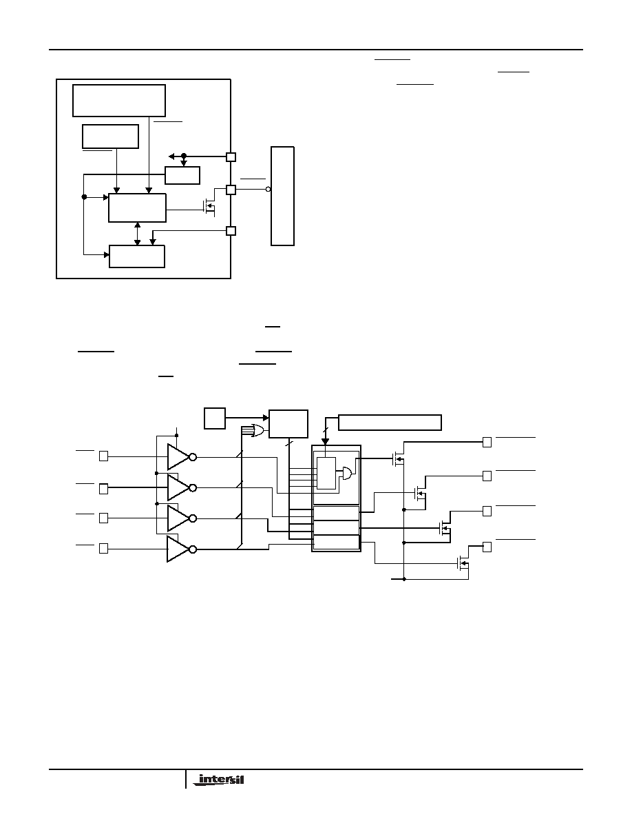
Overcurrent Protection (Circuit Breaker Function)
The X80010 over-current circuit provides the following
functions:
- Over-current shut-down of the power FET and external
power good indicators.
- Noise filtering of the current monitor input.
- Relaxed over-current limits for initial board insertion.
- Over-current recovery retry operation.
A sense resistor, placed in the supply path between V
EE
and
SENSE (see Figure 30) generates a voltage internal to the
X80010. When this voltage exceeds 50mV an over current
condition exists and an internal "circuit breaker" trips, turning
off the gate drive to the external FET. The actual over-
current level is dependent on the value of the current sense
resistor. For example a 20m
sense resistor sets the over-
current level to 2.5A.
Intersil's X80010 provides a safety mechanism during
insertion of the board into the back plane. During insertion of
the board into the backplane large currents may be induced.
In order to prevent premature shut down, the overcurrent
detect circuit of the X80010 allows up to 3 times the standard
overcurrent setting during insertion.
After the PWRGD signal is asserted, the X80010 switches
back to the normal overcurrent setting. The over-current
threshold voltage during insertion is 150mV.
After the Power FET turns off due to an over-current
condition, a retry circuit turns the FET back on after a delay
of 100ms. If the over-current condition remains, the FET
again turns off. For the X80010 and X80012, this sequence
repeats indefinitely until the over-current condition is
released. For the X80011 and X80013, the X80010 retries
five times, then, sets an output signal, FAR, to indicate a
failure after retry.
Over-current shut-down
As shown in Figure 35, this circuit block contains a resistor
divider, a comparator, a noise filter and a voltage reference
to monitor for over-current conditions.
The overcurrent voltage threshold (V
OC
) is 50mV. This can
be factory set, by special order, to any setting between
30mV and 100mV. V
OC
is the voltage between the SENSE
and V
EE
pins and across the R
SENSE
resistor. If the
selected sense resistor is 20mW, then 50mV corresponds to
an overcurrent of 2.5A.
If an over-current condition is detected, the GATE is turned
off and all power good indicators go inactive.
Overcurrent Noise Filter
The X80010 has a noise (low pass) filter built into the over-
current comparator. The comparator will thus require the
current spikes to exceed the overcurrent limit for more than
5µs.
Overcurrent During Insertion
Insertion is defined as the first plug-in of the board to the
backplane. In this case, the X80010 is initially fully powered
off prior to the hot plug connection to the mains supply. This
condition is different from a situation where the mains supply
has temporarily failed resulting in a partial recycle of the
power. This second condition will be referred to as a power
cycle.
During insertion, the board can experience high levels of
current for short periods of time as power supply capacitors
charge up on the power bus. To prevent the over-current
sensor from turning off the FET inadvertently, the X80010
has the ability to allow more current to flow through the
powerFET and the sense resistor for a short period of time
until the FET turns on and the PWRGD signal goes active. In
the X80010, 150mV is allowed across sense resistor the
during insertion (10A assuming a 20m
resistor). This
provides a mechanism to reduce insertion issues associated
with huge current surges.
Overcurrent/
Gate
Short-Circuit
Retry Logic
RETRY
Voltage
5µs
noise
38R
3R
+
≠
-48V
Overcurrent Event
R
Sense
Reference
Delay
Control
Block
filtering
FIGURE 35. OVERCURRENT DETECTION/SHORT CIRCUIT
PROTECTION
X80010, X80011, X80012, X80013

17
FN8149.0
January 13, 2005
Hardshort Protection - FET Turn-on Retry
In the event on an over-current or hard short condition, the
X80010 includes a retry circuit. This circuit waits for 100ms,
then attempts to again turn on the FET. If the fault condition
still exists, the FET turns off and the sequence repeats. For
the X80010 and X80012, this process continues indefinitely
until the overcurrent condition does not exist. For the X80011
and X80013, this process repeats five times, only then will
keep the FET off and set the FAR pin active. After FAR is
asserted, it can be cleared using the master reset pin, MRH
(upon MRH assertion the FAR output is cleared) or cycling
the power on V
DD
.
If an overcurrent condition does not occur on any retry, the
gate pin proceeds to open at the user defined slew rate.
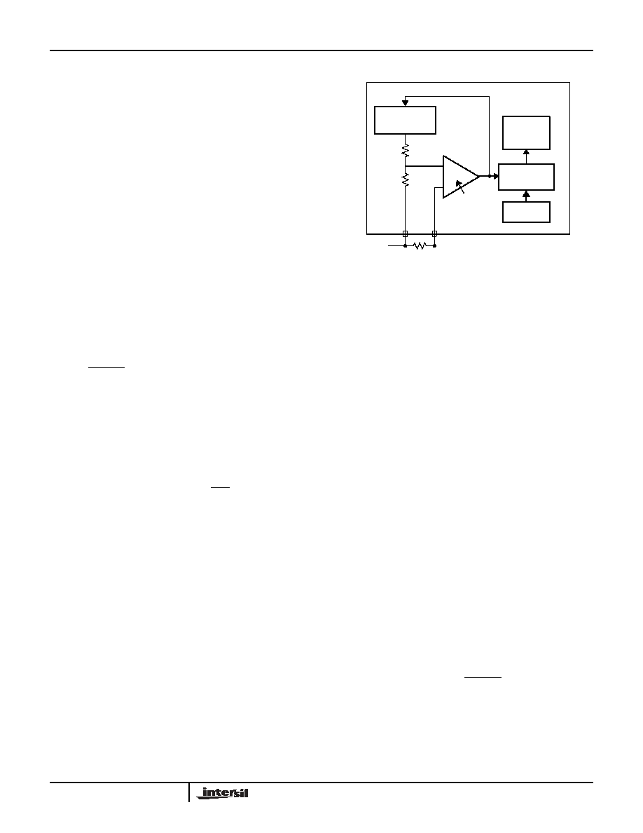
Gate Drive Output Slew Rate (Inrush Current)
Control
The gate output drives an external N-Channel FET. The
GATE pin goes high when no overcurrent, undervoltage or
overvoltage conditions exist.
The X80010 provides an I
GATE
current of 50µA to provide
on-chip slew rate control to minimize inrush current. This
I
GATE
current limits the inrush current and provides the best
charge time for a given load, while avoiding overcurrent
conditions.
For applications that require different ramp rates during
insertion and start-up and operations modes, the X80010
provides two external pins, IGQ1 and IGQ0, that allow the
user to switch to different GATE currents on-the-fly by
selecting one of four pre-selected I
GATE
currents. When
IGQ0 and IGQ1 are left unconnected, the gate current is
50µA. The other three settings are 10µA, 70µA and 150µA
(See Figure 36). Typically, the delay from IGQ1 and IGQ0
selection to a change in the GATE pin current is less than
1
µs.
Slew Rate (Gate) Control
As shown in Figure 37, this circuit block contains a current
source (I
GATE
) that drives the 50µA current into the GATE
pin. This current provides a controlled slew rate for the FET.
For applications that require different ramp rates during
insertion and operation or for applications where a different
gate current is desired, the X80010 provides two external
pins, IGQ1 and IGQ0, that allow the system to switch to a
different GATE current with pre-selected options.
The IGQ1 and IGQ0 pins can be used to select from one of
four set values.
Typically, the delay from IGQ1 and IGQ0 selection to a
change in the GATE pin current is less than 1
µs.
Gate Capacitor, Filtering and Feedback
In Figure 37, the FET control circuit includes an FET
feedback capacitor C
2
, which provides compensation for the
FET during turn on. The capacitor value depends on the
load, the FET gate current, and the maximum desired inrush
current.
The value of C2 can be selected with the following formula.
Where:
I
GATE
= FET Gate current
I
INRUSH
= Maximum desired inrush current
C
LOAD
= DC/DC bulk capacitance
In
rush Curren
t
overcurrent
I
GATE
I
GATE
= 150µA
70µA
50µA
10µA
T1
Time, ms
T2
T3
T4
T5
FIGURE 36. SELECTING I
GATE
CURRENT FOR SLEW RATE
CONTROL ON THE GATE PIN
IGQ1
PIN
IGQ0
PIN
CONTENTS
0
0
Defaults to gate current 50
µA
0
1
Gate Current is 10
µA
1
0
Gate Current is 70
µA
1
1
Gate Current is 150
µA
SENSE
V
EE
R
SENSE
LOAD
V
DD
=12V
Slew
Selection
GATE
10µA
I
INRUSH
DRAIN
100K
Gate Current
IGQ1
IGQ0
-48V
Control
Registers
150µA
Logic
Rate
Quick Select
Logic
100*
100nF*
* Optional Components
See Section "Gate Capacitor, Filtering and Feedback"
22K
3.3nF
C2
R2
50µA
70µA
FIGURE 37. SLEW RATE (INRUSH CURRENT) CONTROL
C2
I
GATE
C
◊
LOAD
I
INRUSH
-------------------------------------------
=
X80010, X80011, X80012, X80013
18
FN8149.0
January 13, 2005
With the X80010, there is some control of the gate current
with the IGQ pins, so one selection of C2 can cover a wide
range of possible loading conditions. Typical values for C2
range from 2.2 to 4.7nF.
When power is applied to the system, the FET tries to turn
on due to its internal gate to drain capacitance (Cgd) and the
feedback capacitor C2 (see Figure 37.) The X80010 device,
when powered, pulls the gate output low to prevent the gate
voltage from rising and keep the FET from turning on.
However, unless V
DD
powers up very quickly, there will be a
brief period of time during initial application of power when
the X80010 circuits cannot hold the gate low. The use of an
external capacitor (C1) prevents this. Capacitors C1 and C2
form a voltage divider to prevent the gate voltage from rising
above the FET turn on threshold before the X80010 can hold
the gate low. Use the following formula for choosing C1.
Where:
V1 = Maximum input voltage,
V2 = FET threshold voltage,
C1 = Gate capacitor,
C2 = Feedback capacitor.
In a system where V
DD
rises very fast, a smaller value of C1
may suffice as the X80010 will control voltage at the gate
before the voltage can rise to the FET turn on threshold. The
circuit of Figure 37 assumes that the input voltage can rise to
80V before the X80010 sees operational voltage on V
DD
. If
C1 is used then the series resistor R1 will be required to
prevent high frequency oscillations.
Drain Sense and Power Good Indicator
The X80010 provides a drain sense and power good
indicator circuit. The PWRGD signal asserts LOW when
there is no overvoltage, no undervoltage, and no overcurrent
condition, the Gate voltage exceeds VDD-1V, and the
voltage at the DRAIN pin is less V
EE
+V
DRAIN
.
As shown in Figure 38, this circuit block contains a drain
sense voltage trip point (
V
DRAIN
) and a gate voltage trip
point (
V
GATE
), two comparators, and internal voltage
references. These provide both a drain sense and a gate
sense circuit to determine the whether the FET has turned
on as requested. If so, the power good indicator (PWRGD)
goes active.
The drain sense circuit checks the DRAIN pin. If the voltage
on this pin is greater that 1V above V
EE
, then a fault
condition exists.
The gate sense circuit checks the GATE pin. If the voltage
on this pin is less than V
EE
- 1V, then a fault condition exists.
The PWRGD signal asserts (Logic LOW) only when all of the
below conditions are true:
- there is no overvoltage or no undervoltage condition,
(i.e. undervoltage < V
EE
< overvoltage.)
- There is no overcurrent condition (i.e. V
EE
- V
SENSE
<
V
OC
.)
- The FET is turned on (i.e. V
DRAIN
< V
EE
+ 1V and
V
GATE
> V
DD
- 1V).
Power On/System Reset and Delay
Application of power to the X80010 activates a Power On
Reset circuit that pulls the RESET pin active. This signal, if
used, provides several benefits.
- It prevents the system microprocessor from starting to
operate with insufficient voltage.
- It prevents the processor from operating prior to
stabilization of the oscillator.
- It allows time for an FPGA to download its configuration
prior to initialization of the circuit.
The POR/RESET circuit is activated when all voltages are
within specified ranges and the following time-out conditions
are met: PWRGD and V1GOOD, V2GOOD, V3GOOD, and
V4GOOD. The POR/RESET circuit will then wait 100ms and
assert the RESET pin.
C1
V1 V2
≠
V2
---------------------C2
=
(Factory
Programmable)
SENSE
V
EE
R
SENSE
LOAD
GATE
DRAIN
100K
-48V
PWRGD
+
≠
1V
V
EE
Control/Status
Registers
Power
Good
Logic
V
DRAIN
+
≠
VDD-1V
V
GATE
FIGURE 38. DRAIN SENSE AND POWER GOOD INDICATOR
X80010, X80011, X80012, X80013
19
FN8149.0
January 13, 2005
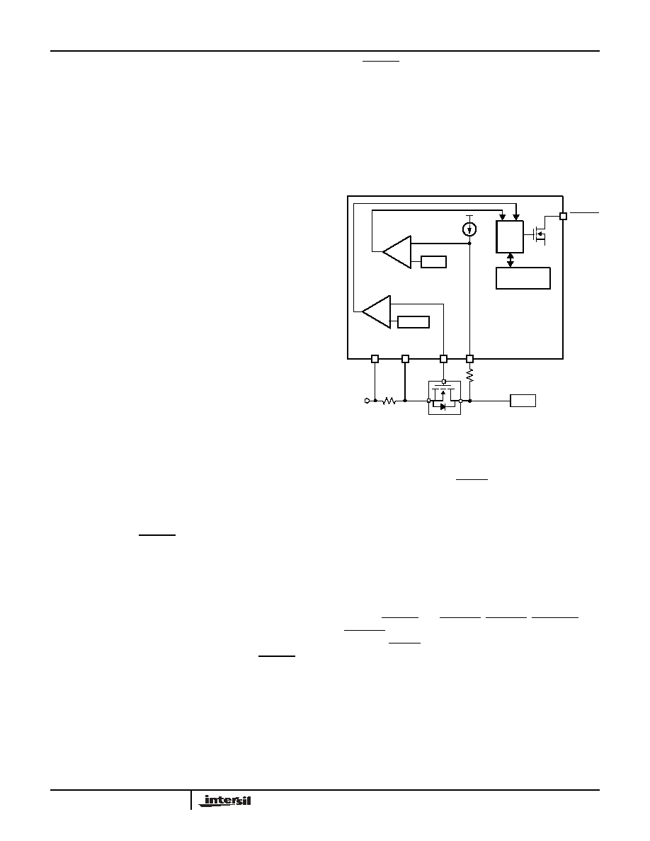
Quad Voltage Monitoring
X80010 monitors 4 voltage enable inputs. When the ENi
(i=1-4) input is detected to be below the input threshold, the
output ViGOOD (i = 1 to 4) goes active LOW. The ViGOOD
signal is asserted after a delay of 100ms. The ViGOOD
signal remains active until ENi rises above threshold.
Once the PWRGD signal is asserted, the power sequencing
of the DC/DC modules can commence. RESET goes active
100ms after all ViGOOD (i=1 to 4) outputs are asserted (See
Figure 39).
As shown in Figure 40, this circuit block contains four
separate voltage enable pins, a time delay circuit, and an
output driver.
Control
Registers
RESET Logic
SPOR
MRC
V
DD
Drain Sense
& Power
Good Logic
Enable
Logic
t
SPOR
Delay
RESET
PWRGD
ViGOOD
i = 1 to 4
µ
P
V
EE
FIGURE 39. POWER ON/SYSTEM RESET AND DELAY
EN1
EN2
EN3
EN4
V4GOOD
V3GOOD
V2GOOD
V1GOOD
V
EE
Divider
4
Reset
OSC
0.1s
0.5s
1s
5s
Select
4
delay1
delay2
delay3
delay4
Delay circuit
repeated 4 times
V
RGO
Control Register
FIGURE 40. VOLTAGE MONITORS AND VGOOD OUTPUTS
X80010, X80011, X80012, X80013

20
FN8149.0
January 13, 2005
Manual Reset (Hot Side and Cold Side)
The manual reset option allows a hardware reset of either
the Gate control or the PWRGD indicator. These can be
used to recover the system in the event of an abnormal
operating condition.The X80010 has two manual reset pins:
MRH (manual reset hot side) and MRC (manual reset cold
side). The MRH signal is used as a manual reset for the
GATE pin. This pin is used to initiate Soft Reinsert. When
MRH is pulled LOW the GATE pin will be pulled LOW. It also
clears the FAR signal. When the MRH pin goes HIGH, it
removes the override signal and the gate will turn on based
on the selected gate control mechanism.
The MRC signal is used as a manual reset for the PWRGD
signal. This pin is used to initiate a Soft Restart. When the
MRC is pulled HIGH, the PWRGD signal is pulled HIGH.
When MRC pin goes LOW, the PWRGD pin goes
operational. It will go LOW if all constraints on the GATE are
within limits.
Flexible Power Sequencing of Multiple Power
Supplies
The X80010 provides several circuits such as multiple
voltage enable pins, programmable delays, and a power
good signals can be used to set up flexible power
sequencing schemes for downstream DC/DC supplies.
Below are examples of parallel and relay sequencing.
1. Power Up of DC/DC Supplies In Parallel Sequencing
Using Programmable Delays on Power Good (See Figure
41 and Figure 42).
Several DC/DC power supplies and their respective
power up start times can be controlled using the X80010
such that each of the DC/DC power supplies will start up
following the issue of the PWRGD signal. The PWRGD
signal is fed into the ENi inputs to the X80010. When
PWRGD is valid, the internal voltage enable circuits issue
ViGOOD signals after a time delay. The ViGOOD signals
control the ON/OFF pins of the DC/DC supplies. Each
DC/DC converter is instructed to turn on 100ms after the
PWRGD goes active. However, each ViGOOD delay can
be increased with the use of external R-C circuits.
TABLE 3. MANUAL RESET OF THE HOT SIDE (GATE SIGNAL)
MRH
GATE PIN
REQUIREMENTS
1
Operational When
MRH is HIGH the Manual Reset
(Hot) function is disabled
0
OFF
MRH must be held LOW minimum of 5
µs
TABLE 4. MANUAL RESET OF THE COLD SIDE (PWRGD
SIGNAL)
MRC
PWRGD
REQUIREMENTS
1
HIGH
MRC must be held HIGH minimum of 5
µs
0
Operational When MRC is LOW the MRC
function is disabled
X80010, X80011, X80012, X80013

21
FN8149.0
January 13, 2005
V
DD
V3GOOD
EN3
V2GOOD
EN2
V1GOOD
EN1
PWRGD
X80010, X80011,
V
UV/OV
V
EE
SENSE
DRAIN
-48V
UV=37V
OV=71V
-48V
GATE
Rs
0.02
5%
ON/OFF
C3
0.1µF
100V
C4
100µF
100V
1
4
V
IN+
V
IN-
V
OUT
+
V
OUT
SENSE+
TRIM
SENSE-
+
9
8
7
6
5
RESET
µC
V
CC1
3.3V
GND
ON/OFF
C6
0.1µF
100V
C7
100µF
100V
1
4
V
IN+
V
IN-
V
OUT
+
V
OUT
SENSE+
TRIM
SENSE-
+
9
8
7
6
5
FPGA
V
CC1
2.5V
GND
ON/OFF
C9
0.1µF
100V
C10
100µF
100V
1
4
V
IN+
V
IN-
V
OUT
+
V
OUT
SENSE+
TRIM
SENSE-
+
9
8
7
6
5
ASIC
V
CC1
1.8V
GND
R4
182k
1%
R5
30k
1%
R6
10k
1%
Q1
IRFR120
C5
100µF
16V
C8
100µF
16V
C11
100µF
16V
+
+
+
V4GOOD
EN4
ON/OFF
C12
0.1µF
100V
C13
100µF
100V
1
4
V
IN+
V
IN-
V
OUT
+
V
OUT
SENSE+
TRIM
SENSE-
+
9
8
7
6
5
1.2V
GND
C14
100µF
16V
+
RESET
OPTO
COUPLER
PWRGD
RESET `
V
CC2
V
CC2
V
CC2
MRH
MRC
Return
OPTO
COUPLER
0.1µF
100
4.7K
3.3n
100K
FIGURE 41. TYPICAL APPLICATION OF HOTSWAP AND DC/DC PARALLEL POWER SEQUENCING
X80013, X80014
X80010, X80011, X80012, X80013
22
FN8149.0
January 13, 2005
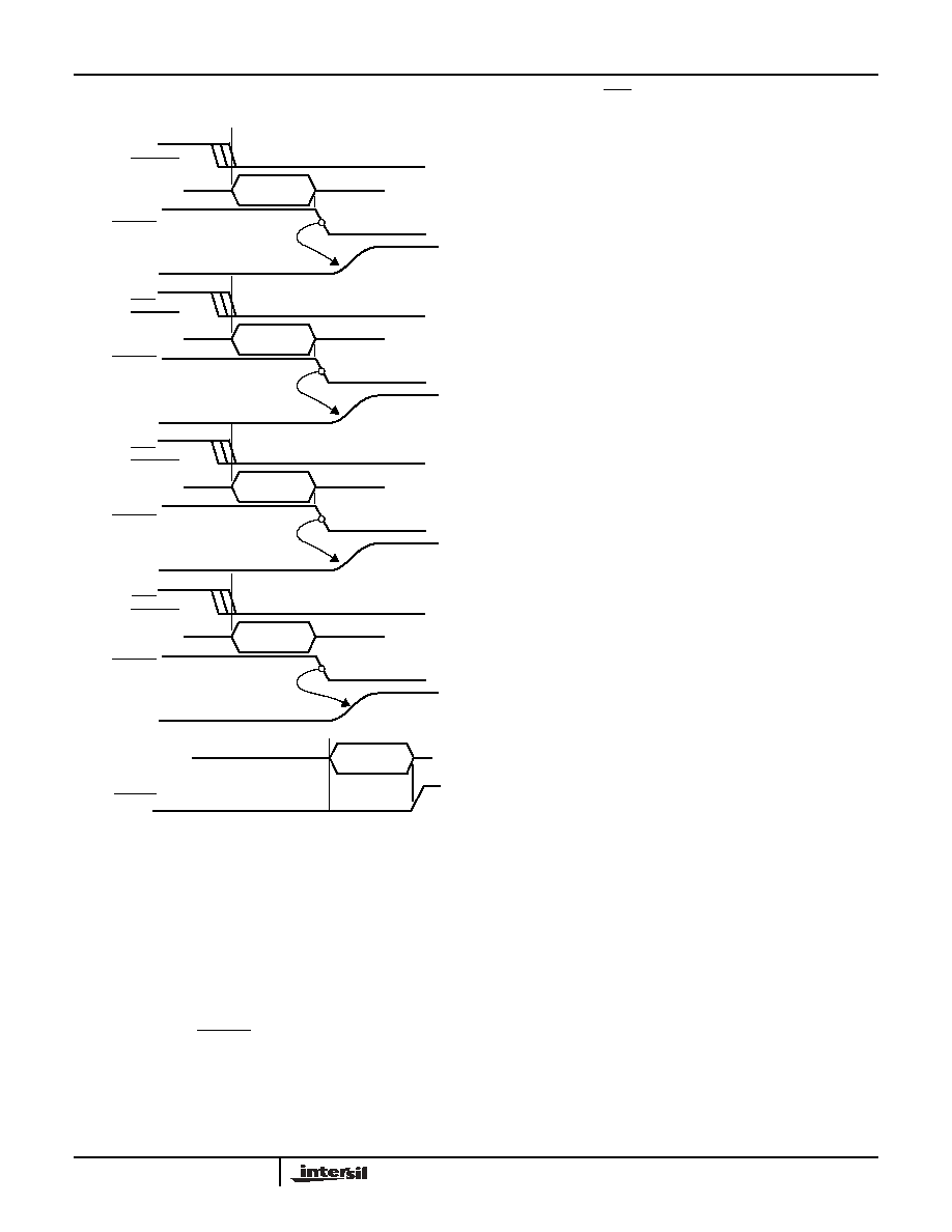
1. Power Up of DC/DC Supplies Via Relay Sequencing
Using Power Good and Voltage Monitors (see Figure 43
and Figure 44).
Several DC/DC power supplies and their respective
power up start times can be controlled using the X80010
such that each of the DC/DC power supplies will start in
a relay sequencing fashion. The 1st DC/DC supply will
power up when PWRGD is LOW after a 100ms delay.
Subsequent DC/DC supplies will power up after the prior
supply has reached its operating voltage. One way to do
this is by using an external CPU Supervisor (for example
the Intersil X40430) to monitor the DC/DC output. When
the DC/DC voltage is good, the supervisor output signals
the X80010 EN1 input to sequence the next supply. An
opto-coupler is recommended in this connection for
isolation. This configuration ensures that each
subsequent DC/DC supply will power up after the
preceding DC/DC supply voltage output is valid.
EN1
t
DELAY1
V1GDO
Power Supply
#1 turns ON
Power Supply
V2GDO
100ms
V3GDO
#1 OUTPUT
t
DELAY2
t
DELAY3
Power Supply
#2 OUTPUT
Power Supply
#3 OUTPUT
t
DELAY4
V4GDO
(from PWRGD)
(3.3V)
(2.5V)
(1.8V)
RESET
Main FET
turns ON
EN2
EN3
Power Supply
#4 OUTPUT
(1.2V)
EN4
Power Supply
#2 turns ON
100ms
Power Supply
#3 turns ON
100ms
Power Supply
#4 turns ON
100ms
100ms
t
SPOR
All ViGOOD=LOW
(from PWRGD)
(from PWRGD)
(from PWRGD)
FIGURE 42. PARALLEL SEQUENCING OF DC/DC SUPPLIES.
(TIMING)
X80010, X80011, X80012, X80013

23
FN8149.0
January 13, 2005
V
DD
V3GOOD
EN3
V2GOOD
EN2
V1GOOD
EN1
PWRGD
X80010, X80011,
V
UV/OV
V
EE
SENSE
DRAIN
-48V
UV=37V
OV=71V
-48V
GATE
Rs
0.02
5%
100
ON/OFF
C3
0.1µF
100V
C4
100µF
100V
1
4
V
IN+
V
IN-
V
OUT
+
V
OUT
SENSE+
TRIM
SENSE-
+
9
8
7
6
5
3.3V
GND
ON/OFF
C6
0.1µF
100V
C7
100µF
100V
1
4
V
IN+
V
IN-
V
OUT
+
V
OUT
SENSE+
TRIM
SENSE-
+
9
8
7
6
5
2.5V
GND
ON/OFF
C9
0.1µF
100V
C10
100µF
100V
1
4
V
IN+
V
IN-
V
OUT
+
V
OUT
SENSE+
TRIM
SENSE-
+
9
8
7
6
5
1.8V
GND
R4
182k
1%
R6
10k
1%
Q1
IRFR120
C5
100µF
16V
C8
100µF
16V
C11
100µF
16V
+
+
+
V4GOOD
EN4
ON/OFF
C12
0.1µF
100V
C13
100µF
100V
1
4
V
IN+
V
IN-
V
OUT
+
V
OUT
SENSE+
TRIM
SENSE-
+
9
8
7
6
5
1.2V
GND
C14
100µF
16V
+
RESET
OP
T
O
COUPL
E
R
RESET
X40430
OPTO
COUPLER
VMON<1:3>
VF
AI
L<1
:
3>
PWRGD
RESET
µC
V
CC1
FPGA
V
CC1
ASIC
V
CC1
V
CC2
V
CC2
V
CC2
MRH
MRC
R5
30k
1%
Return
OPTO
COUPLER
0.1µF
4.7K
3.3n
100K
FIGURE 43. TYPICAL APPLICATION OF HOTSWAP AND DC/DC RELAY SEQUENCING
X80012, X80013
X80010, X80011, X80012, X80013

24
All Intersil U.S. products are manufactured, assembled and tested utilizing ISO9000 quality systems.
Intersil Corporation's quality certifications can be viewed at www.intersil.com/design/quality
Intersil products are sold by description only. Intersil Corporation reserves the right to make changes in circuit design, software and/or specifications at any time without
notice. Accordingly, the reader is cautioned to verify that data sheets are current before placing orders. Information furnished by Intersil is believed to be accurate and
reliable. However, no responsibility is assumed by Intersil or its subsidiaries for its use; nor for any infringements of patents or other rights of third parties which may result
from its use. No license is granted by implication or otherwise under any patent or patent rights of Intersil or its subsidiaries.
For information regarding Intersil Corporation and its products, see www.intersil.com
FN8149.0
January 13, 2005
EN2 In
t
DELAY1
V1GDO
Power Supply
#1 turns ON
Power Supply
V2MON
threshold
Power Supply
#3 turns ON
V2GDO
100ms
V3GDO
#1 OUTPUT
100ms
t
DELAY2
Power Supply
#2 turns ON
V3MON
threshold
100ms
t
DELAY3
Power Supply
#2 OUTPUT
V4MON
Power Supply
#3 OUTPUT
threshold
t
DELAY4
V4GDO
(from PWRGD)
(3.3V)
(2.5V)
(1.8V)
t
RESET
RESET
100ms
100ms
FET
turns ON
EN2
EN3
Power Supply
#4 OUTPUT
(1.2V)
EN4
Power Supply
#4 turns ON
FIGURE 44. RELAY SEQUENCING OF DC/DC SUPPLIES. (TIMING)
X80010, X80011, X80012, X80013
25
FN8149.0
January 13, 2005
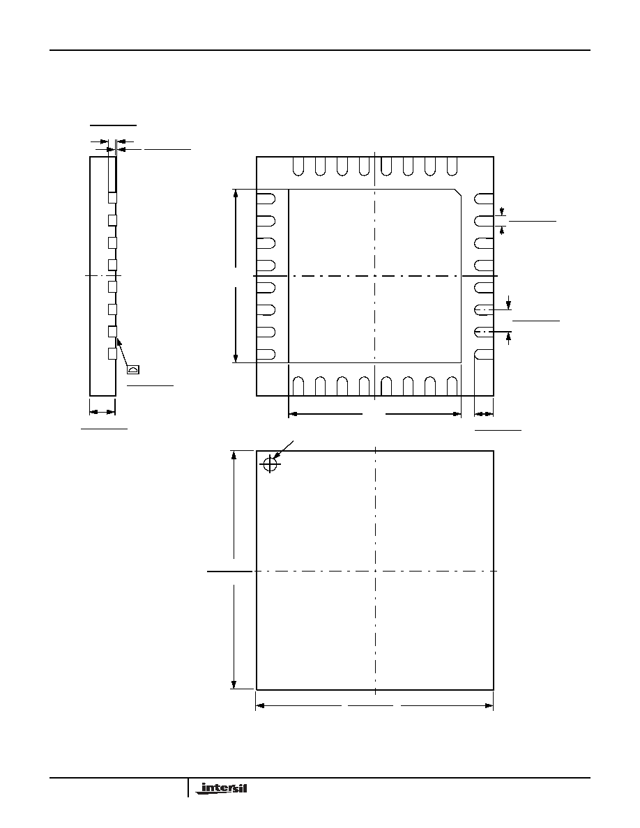
Packaging Information
0.009 (0.23)
0.015 (0.38)
0.185
(4.70)
0.271 (6.90)
0.279 (7.10)
0.014 (0.35)
0.029 (0.75)
(4.70)
0.185
(4.70)
0.027 (0.70)
0.031 (0.80)
0.000 (0.00)
0.030 (0.76)
0.007 (0.19)
0.009 (0.25)
0.000 (0.00)
0.002 (0.05)
0.271 (6.90)
0.279 (7.10)
0.271 (6.90)
0.279 (7.10)
PIN 1 INDENT
32-Lead Very Very Thin Quad Flat No Lead Package
7mm x 7mm Body with 0.65mm Lead Pitch
X80010, X80011, X80012, X80013