 | –≠–ª–µ–∫—Ç—Ä–æ–Ω–Ω—ã–π –∫–æ–º–ø–æ–Ω–µ–Ω—Ç: X80073 | –°–∫–∞—á–∞—Ç—å:  PDF PDF  ZIP ZIP |

1
Æ
FN8150.0
CAUTION: These devices are sensitive to electrostatic discharge; follow proper IC Handling Procedures.
1-888-INTERSIL or 1-888-352-6832
|
Intersil (and design) is a registered trademark of Intersil Americas Inc.
Copyright Intersil Americas Inc. 2005. All Rights Reserved
All other trademarks mentioned are the property of their respective owners.
X80070, X80071, X80072, X80073
Hot Swap Controller with
Advanced Fault Protection and
Voltage Regulator Output
FEATURES
∑ Hot swap controller
-- Overvoltage and undervoltage protection
-- Undervoltage lockout for battery/redundant supplies
-- Electronic circuit breaker
-- Slew Rate for External FET Gate Control
-- Overcurrent Detection and Gate Shut-off
-- 3X overcurrent limit on insertion
-- 5µs overcurrent filter
-- Hardshort Retry and Indicator
-- Typically operates from -30V to -80V. Tolerates tran-
sients to -200V (limited by external components)
-- Positive Voltages (low side switching) from 12V to 60V
-- Soft Re-insertion
-- Soft extraction
∑ Battery backup mode
∑ Hardshort retry
∑ Overcurrent Filter
∑ Insertion Limits.
∑ Selectable Gate Current
∑ Voltage Regulator Output for Supervisory Functions
∑ Debounced manual reset input
∑ Available packages
-- 20-lead Quad No-Lead Frame (QFN)
APPLICATIONS
∑ -48V Hot Swap Power Backplane/Distribution Central
Office, Ethernet for VOIP
∑ Positive Voltage Hotswap 12V to 60V Applications
(low side switching)
∑ Card Insertion Detection
∑ IP Phone Applications
∑ Databus Power Interfacing
∑ Custom Industrial Power Backplanes
∑ Distributed Power Systems
DESCRIPTION
The X80070 is a hot swap controller that allows a board to be
safely inserted and removed from a live backplane without
turning off the main power supply.
During insertion, the gate of an external power MOSFET is
clamped low to suppress contact bounce. The
undervoltage/overvoltage circuits and the power-on reset
circuitry suppress the gate turn on until the mechanical bounce
has ended. The X80070 turns on the gate with a slew rate to
limit the inrush current and incorporates an electronic circuit
breaker set by a sense resistor. After the load is successfully
charged, the PWRGD signal is asserted; indicating that the
device is ready to power sequence the DC-DC power bricks.
At all times, the X80070 monitors for undervoltage, overvoltage,
and overcurrent conditions. If any fault occurs, the gate will be
immediately shut off and the PWRGD will be returned to the
inactive state. The X80070 contains overvoltage, undervoltage
and overcurrent detection, hardshort retry, gate control slew
rate and power good control.
TYPICAL APPLICATION
V
DD
X80070
V
UV/OV
V
EE
SENSE
UV=43V
OV=75V
-48V
GATE
Rs
0.02
5%
R4
182k
1%
R5
30k
1%
R6
10k
1%
Q1
IRFR120
DC-DC
Module
1
ON/OFF
PWRGD
100
22K
3.3n
100n
V
RGO
I
GQ1
I
GQ0
Gate
Current
Select
-48V
Return
*
*
*
*
Optional components
Depends on choice of DC-DC Module
Data Sheet
March 15, 2005

2
FN8150.0
March 15, 2005
ORDERING INFORMATION
ABSOLUTE MAXIMUM RATINGS
Temperature under bias ..............................-65∞C to +135∞C
Storage temperature ...................................-65∞C to +150∞C
Voltage on given pin (Hot Side Functions):
V
ov / uv pin
............................................................ 5.5V + V
EE
SENSE pin ...................................................... 400mV + V
EE
V
EE
pin .......................................................................... -80V
PWRGD pin........................................................... 7 V + V
EE
GATE pin.............................................................. V
DD
+ V
EE
FAR pin .................................................................. 7V + V
EE
MR pin ................................................................. 5.5V + V
EE
BATT-ON pin....................................................... 5.5V + V
EE
Voltage on given pin (Cold Side Functions):
IGQ1 and IGQ0 pins............................................ 5.5V + V
EE
V
DD
pin ................................................................. 14V + V
EE
D.C. output current ........................................................ 5mA
Lead temperature (soldering, 10 seconds)..................300∞C
COMMENT
Stresses above those listed under "Absolute Maximum
Ratings" may cause permanent damage to the device. This is a
stress rating only; functional operation of the device (at these or
any other conditions above those listed in the operational
sections of this specification) is not implied. Exposure to
absolute maximum rating conditions for extended periods
may affect device reliability.
RECOMMENDED OPERATING CONDITIONS
ORDER
NUMBER
OV
(V)
UV1
(V)
UV2
(V)
t
NF
(us)
V
OC
(mV)
V
OCI
(mV)
Over-
current
Retry
Retry
Delay
(ms)
I
GATE
(uA)
T
DELAY
(ms)
t
POR
(ms)
Temp
PART
MARK
X80070Q20I
74.9
42.4
33.2
5
50
150
Always
100
50
100
100
-40
o
C to 85
o
C 80070I
X80071Q20I
68.0
42.4
33.2
5
50
150
Always
100
50
100
100
-40
o
C to 85
o
C 80071I
X80072Q20I
74.9
42.4
33.2
5
50
150
5 retries
100
50
100
100
-40
o
C to 85
o
C 80072I
X80073Q20I
68.0
42.4
33.2
5
50
150
5 retries
100
50
100
100
-40
o
C to 85
o
C 80073I
QFN package
(Top view)
I
GQ1
MR
V
RGO
DNC
I
GQ0
DNC
NA
DNC
GATE
NA
V
UV/OV
SE
N
S
E
FAR
PW
RGD
BA
TT-O
N
V
DD
DNC
DNC
DNC
V
EE
1
2
3
4
5
6 7 8 9 10
11
12
13
14
15
16
17
18
19
20
5mm x 5mm
Temperature
Min.
Max.
Industrial
-40∞C
+85∞C
Supply Voltage
V
DD
= 12V
X80070, X80071, X80072, X80073

3
FN8150.0
March 15, 2005
ELECTRICAL CHARACTERISTICS
(Standard Settings)
(Over the recommended operating conditions unless otherwise specified).
Symbol
Parameter
Min.
Typ.
Max.
Unit
Test Conditions
DC Characteristics
V
DD
Supply Operating Range
10
12
14
V
I
DD
Supply Current
2.5
5
mA
V
RGO
Regulated 5V output
4.5
5.5
I
RGO
= 10uA
I
RGO
V
RGO
current output
50
µA
I
GATE
Gate Pin Current
46.2
52.5
58.8
µA Gate Drive On,
V
GATE
= V
EE
,
V
SENSE
= V
EE
(sourcing)
9
mA V
GATE
- V
EE
= 3V
V
SENSE
-V
EE
= 0.1V (sinking)
V
GATE
External Gate Drive (Slew Rate Con-
trol)
V
DD
-1
V
DD
V
I
GATE
= 50uA
V
PGA
Power Good Threshold
(PWRGD High to Low)
0.9
1
1.1
V
Referenced to V
EE
V
UV1
< V
UV/OV
< V
OV
V
IHB
Voltage Input High (BATT-ON)
V
EE
+ 4
V
EE
+ 5
V
V
ILB
Voltage Input Low (BATT-ON)
V
EE
+ 2
V
I
LI
Input Leakage Current (MR, IGQ0,
IGQ1)
10
µA V
IL
= GND to
V
CC
I
LO
Output Leakage Current (PWRGD)
10
µA Gate is Off
V
IL
Input LOW Voltage (MR, IGQ0, IGQ1)
-0.5 + V
EE
(V
EE
+ 5) x 0.3
V
V
IH
Input HIGH Voltage (MR, IGQ0, IGQ1) (V
EE
+ 5)
x 0.7
(V
EE
+ 5) + 0.5
V
V
OL
Output LOW Voltage
(FAR, PWRGD)
V
EE
+
0.4
V
I
OL
= 4.0 mA
(V
EE
+ 2.7 to V
EE
+ 5.5V)
I
OL
= 2.0 mA
(V
EE
+ 2.7 to V
EE
+ 3.6V)
C
OUT
(1)
Output Capacitance (FAR)
8
pF V
OUT
= 0V
C
IN
(1)
Input Capacitance (MR) 6
pF V
IN
= 0V
V
OC
Overcurrent threshold
45
50
55
mV V
OC
= V
SENSE
- V
EE
V
OCI
Overcurrent threshold (Insertion)
135
150
165
mV V
OC
= V
SENSE
- V
EE
PWRGD = HIGH
Initial Power-up condition
V
OVR
Overvoltage threshold (rising)
X80070, X80072
X80071, X80073
3.85
3.49
3.90
3.54
3.95
3.59
V
Referenced to V
EE
V
OVF
Overvoltage threshold (falling)
X80070, X80072
X80071, X80073
3.82
3.46
3.87
3.51
3.92
3.56
V
Referenced to V
EE
V
UV1R
Undervoltage 1 threshold (rising)
2.19
2.24
2.29
V
Referenced to V
EE
BATT-ON = V
EE
V
UV1F
Undervoltage 1 threshold (falling)
2.16
2.21
2.26
V
V
UV2R
Undervoltage 2 threshold (rising)
1.71
1.76
1.81
V
Referenced to V
EE
BATT-ON = V
RGO
V
UV2F
Undervoltage 2 threshold (falling)
1.68
1.73
1.78
V
AC Characteristics
t
FOC
Sense High to Gate Low
1.5
2.5
3.5
µ
s
X80070, X80071, X80072, X80073

4
FN8150.0
March 15, 2005
Notes: (1) This parameter is based on characterization data.
EQUIVALENT A.C. OUTPUT LOAD CIRCUIT
A.C. TEST CONDITIONS
t
FUV
Undervoltage conditions to Gate Low
0.5
1.0
1.5
µ
s
t
FOV
Overvoltage Conditions to Gate Low
1.0
1.5
2
µ
s
t
VFR
Overvoltage/undervoltage failure re-
covery time to Gate =1V.
1.2
1.6
2
µ
s
V
DD
does not drop below 3V,
No other failure conditions.
t
BATT-ON
Delay BATT-ON Valid
100
ns
t
MR
Minimum time high for reset valid on
the MR pin
5
µ
s
t
MRE
Delay from MR enable to Gate Pin
LOW
1.0
1.6 2.4
µ
s
I
GATE
= 60µA, No Load
t
MRD
Delay from MR disable to GATE
reaching 1V
1.8
2.6
µ
s
I
GATE
= 60µA, No Load
t
QC
Delay from IGQ1 and IGQ0 to valid
Gate pin current
1
µ
s
t
SC_RETRY
Delay between Retries
90
100
110
ms
t
NF
Noise Filter for Overcurrent
4.5
5
5.5
µs
t
DPOR
Device Delay before Gate assertion
45
50
55
ms
Input pulse levels
V
CC
x 0.1 to
V
CC
x 0.9
Input rise and fall times
10ns
Input and output timing levels
V
CC
x 0.5
Output load
Standard output load
ELECTRICAL CHARACTERISTICS
(Standard Settings)
(Continued)
(Over the recommended operating conditions unless otherwise specified).
Symbol
Parameter
Min.
Typ.
Max.
Unit
Test Conditions
5V
4.6k
30pF
FAR
PWRGD
X80070, X80071, X80072, X80073

5
FN8150.0
March 15, 2005
Figure 1. Overvoltage/Undervoltage GATE Timing
Figure 2. Overcurrent GATE Timing
Figure 3. Manual Reset
SENSE
V
UV/OV
V
OV
V
UV
V
DD
V
TH
MR
GATE
V
OC
V
OCI
t
VFR
t
FOV
t
FUV
t
DPOR
t
VFR
1V
1V
SENSE
V
DD
V
TH
GATE
V
OC
V
OCI
t
DPOR
t
SC_RETRY
t
FOC
t
FOC
Always Retry
V
UV <
V
UV/OV <
V
OV
t
SC_RETRY
MR = HIGH
t
MRD
GATE
t
MRE
MR
t
MR
1V
X80070, X80071, X80072, X80073

6
FN8150.0
March 15, 2005
TYPICAL PERFORMANCE CHARACTERISTICS
Overcurrent Threshold vs. Temperature
Overvoltage Threshold vs. Temperature
Undervoltage 1 Threshold vs. Temperature
Undervoltage 2 Threshold vs. Temperature
I
GATE
(source) vs. Temperature
I
GATE
(sink) vs. Temperature
46.000
47.000
48.000
49.000
50.000
51.000
52.000
-55 -40 -25 -10
5
20
35
50
65
80
95 110 125
Temperature
In
rus
h
C
u
rre
nt L
i
m
i
t (mV
)
3.85
3.86
3.87
3.88
3.89
3.90
3.91
3.92
-55 -40 -25 -10 5
20
35
50
65 80
95 110 125
Temperature
Rising
Falling
O
V
Thr
e
s
ho
ld (V)
2.190
2.200
2.210
2.220
2.230
2.240
2.250
-55 -40 -25 -10
5
20
35 50
65
80
95 110 125
Temperature
Rising
Falling
Undervol
t
a
ge 1
Threshold
(V)
1.690
1.700
1.710
1.720
1.730
1.740
1.750
1.760
1.770
1.780
-55 -40 -25 -10
5
20
35
50 65
80 95 110 125
Temperature
Rising
Falling
Undervol
ta
ge 2
Threshol
d
(V)
0
40
80
120
160
200
-55 -40 -25 -10
5
20
35
50 65
80
95 110 125
Temperature
150µA
70µA
50µA
10µA
G
a
te Current (µA)
7.0
7.5
8.0
8.5
9.0
9.5
10.0
10.5
11.0
-55 -40 -25 -10
5
20 35
50
65 80
95 110 125
Temperature
Ga
te Current - Si
n
k
(mA)
X80070, X80071, X80072, X80073

7
FN8150.0
March 15, 2005
t
FUV
vs. Temperature
t
FOV
vs. Temperature
t
FOC
vs. Temperature
0.500
0.550
0.600
0.650
0.700
0.750
0.800
-55 -40 -25 -10
5
20 35
50
65
80
95 110 125
Temperature
tUV1
tUV2
t
UV
(µs)
1.0
1.1
1.1
1.2
1.2
1.3
1.3
1.4
1.4
-55 -40 -25 -10
5
20
35
50
65 80
95 110 125
Temperature
t
OV
(µs)
1.7
1.8
1.9
2.0
2.1
2.2
2.3
2.4
2.5
-55 -40 -25 -10 5
20
35
50
65 80
95 110 125
Temperature
t
OC
(µ
s
)
X80070, X80071, X80072, X80073

8
FN8150.0
March 15, 2005
Figure 4. Block Diagram
SENSE
V
EE
GATE
IGQ1
IGQ0
BATT-ON
MR
V
DD
FAR
PWRGD
Power Good
Logic
Slew Rate
Selection
5V reg
V
RGO
V
EE
V
EE
V
OV
Ref
V
UV1
Ref
V
UV2
Ref
V
UV/OV
2:1
MUX
V
EE
Gate
Control
V
DD
V
OC
REF
38R
3R
Reset Logic
and Delay
V
EE
Overcurrent logic,
Hard short relay,
Retry logic status
and delay
POR
Timing/
Control logic
50uA
X80070, X80071, X80072, X80073

9
FN8150.0
March 15, 2005
PIN CONFIGURATION
FUNCTIONAL DESCRIPTION
Hot Circuit Insertion
When circuit boards are inserted into a live backplane, the
bypass capacitors at the input of the board's power module or
DC/DC converter can draw huge transient currents as they
charge up. This transient current can cause permanent
damage to the board's components and cause transients on
the system power supply.
The X80070 is designed to turn on a board's supply voltage in a
controlled manner (see Figure 5), allowing the board to be
safely inserted or removed from a live backplane. The device
also provides undervoltage, overvoltage and overcurrent
protection while keeping the power module (dc-dc converter)
off until the backplane input voltage is stable and within
tolerance.
Figure 5. Typical Inrush with Gate Slew Rate Control
PIN DESCRIPTIONS
Pin
Name
Description
1
V
RGO
Regulated 5V output. Used to pull-up
user programmable inputs IGQ0, IGQ1,
BATT-ON and MRH (if needed).
2
DNC
Pin not used. Do not connect to this pin.
3
NA2
Not Available. Connect to V
EE
.
4
NA2
Not Available. Connect to V
EE
.
5
V
DD
Positive Supply Voltage Input.
6
V
EE
Negative Supply Voltage Input.
7
V
UV/OV
Analog Undervoltage and Overvoltage
Input. Turns off the external N-channel
MOSFET when there is an undervoltage
or overvoltage condition.
8
SENSE
Circuit Breaker Sense Input. This input
pin detects the overcurrent condition.
9
GATE
FET Gate Drive. This pin supplies the cur-
rent to turn on the FET.
10
DNC
Pin not used. Do not connect to this pin.
11
DNC
Pin not used. Do not connect to this pin.
12
NA1
Not Available. Connect to V
RGO
.
13
NA1
Not Available. Connect to V
RGO
.
14
NA2
Not Available. Connect to V
EE
.
15
FAR
Failure After Re-try (FAR) output signal.
16
BATT-ON Battery On Input. This input signals that
the battery backup (or secondary supply)
is supplying power to the backplane. It has
an internal pulldown resistor. (>10M
typical)
17
PWRGD Power Good Output. This output pin en-
ables a power module.
X80070
20L QFN Package
I
GQ1
MR
V
RGO
DNC
IG
Q
0
NA2
NA1
DN
C
GATE
NA1
V
UV/OV
SENS
E
FAR
PWRGD
BA
TT-ON
V
DD
NA2
DNC
NA2
V
EE
1
2
3
4
5
6 7 8 9 10
11
12
13
14
15
16
17
18
19
20
TOP VIEW
NA1 pins connect to V
RGO
5mm x 5mm
NA2 pins connect to V
EE
18
IGQ1
Gate Current Quick Select Bit 1 Input.
This pin is used to change the gate current
drive and is intended to allow for current
ramp rate control of the gate pin of an
external FET. It has an internal pulldown
resistor. (>10M
typical)
19
IGQ0
Gate Current Quick Select Bit 0 Input.
This pin is used to change the gate current
drive and is intended to allow for current
ramp rate control of the gate pin of an
external FET. It has an internal pulldown
resistor. (>10M
typical)
20
MR
Manual Reset. Pulling the MR pin LOW
initiates a GATE pin reset (GATE pin
pulled LOW). The MR signal must be held
LOW for 5
µ
secs (minimum).
PIN DESCRIPTIONS
(Continued)
Pin
Name
Description
V
GATE
V
FET_DRAIN
PWRGD
I
INRUSH
X80070, X80071, X80072, X80073

10
FN8150.0
March 15, 2005
Figure 6. Typical -48V Hotswap Application circuit
Overvoltage and Undervoltage Shutdown
The X80070 provides overvoltage and undervoltage protection
circuits.
When an overvoltage (V
OV
) or undervoltage (V
UV1
and V
UV2
)
condition is detected, the GATE pin immediately pulls low
turning off the supply to the system. The undervoltage
threshold V
UV1
applies to the normal operation with a main
supply. The undervoltage threshold V
UV2
assumes the system
is powered by a battery. When using a battery backup, the
BATT-ON pin is pulled to V
RGO
. The default thresholds have
been set so the external resistance values in Figure 6 provide
an overvoltage threshold of 74.9V (X80070 and X80072) or
68V (X80071 and X80073), a main undervoltage threshold of
43V and a battery undervoltage threshold of 33.8V.
As shown in Figure 9, this circuit block contains comparators
and voltage references to monitor for a single overvoltage and
dual undervoltage trip points. The overvoltage and undervoltage
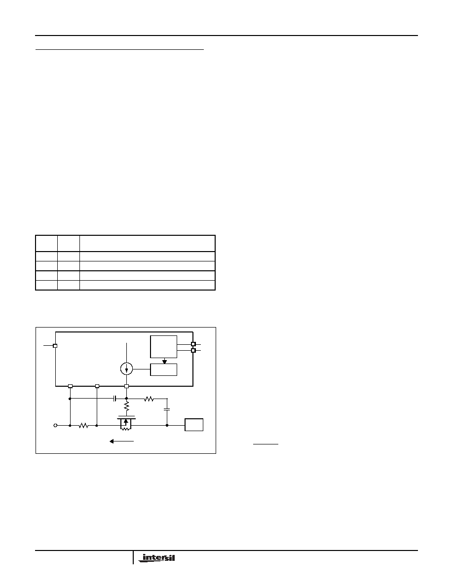
trip points as shown in Table 1 below.
Table 1.
Overvoltage/Undervoltage default thresholds
A resistor divider connected between the plus and minus input
voltages and the V
UV/OV
pin (see Figure 7) determines the
overvoltage and undervoltage shutdown voltages and the
operating voltage range. Using the thresholds in Table 1 and
the equations of Figure 7 the desired operating voltage can be
determined. Figure 8 shows the resistance values for various
operating voltages (X80070 and X80072).
Figure 7. Overvoltage Undervoltage Divider
Figure 8. Operating voltage vs. resistor ratio
Battery back up operations
An external signal, BATT-ON is provided to switch the
undervoltage trip point. The BATT-ON signal is a LOGIC HIGH
if V
IHB
> V
EE
+ 4V and is a LOGIC LOW if V
ILB
< V
EE
+ 2V. The
time from a BATT-ON input change to a valid new undervoltage
threshold is 100ns. See Electrical Specifications for more
details.
Note: The V
UV/OV
pin must be limited to less than V
EE
+ 5.5V.
in worst case conditions. Values for R1 and R2 must be chosen
such that this condition is met. Intersil recommends
R1 = 182k
and R2 = 10k
to conform to factory settings.
These should be 1% resistors.
Table 2.
Selecting between Undervoltage Trip Points
Threshold
Symbol Description falling rising
Max/Min
Voltage
1
Lockout
Voltage
2
V
OV
Overvoltage
(X80070/72)
3.87V 3.9V
74.3
74.9
V
OV
Overvoltage
(X80071/73)
3.51V 3.54V
67.4
68
V
UV1
Undervoltage 1 2.21V 2.24V
43.0
42.4
V
UV2
Undervoltage 2 1.73V 1.76V
33.8
33.2
Notes:
1: Max/Min Voltage is the maximum and mimimum
operating voltage assuming the recommended V
UV/OV
resistor divider.
2: Lockout voltage is the voltage where the X8007x turns
off the FET.
V
DD
X80070
V
UV/OV
V
EE
SENSE
-48V
UV=43V
OV=75V/72V
-48V
GATE
Rs
0.02
5%
R4
182K
1%
R5
30K
1%
R6
10K
1%
Q1
IRFR120
Return
-48V
DC/DC
Converter
I
inrush
PWRGD
ON/OFF
V
RGO
100n
100
22K
3.3n
100uF
10K
Pin
Description
Trip Point Selection
BATT-ON Undervoltage
Trip Point
Selection Pin
If BATT-ON = 0,
V
UV1
trip point is selected;
If BATT-ON = 1,
V
UV2
trip point is selected.
V
UV1
and V
UV2
are undervoltage thresholds.
R1
R2
V
P
V
UV/OV
V
N
Voltage divider:
or:
V
UV OV
/
V
S
R2
R1 R2
+
----------------------
=
V
S
V
UV OV
/
R1 R2
+
R2
----------------------
=
V
S
BATT-ON = V
EE
V
OV
V
UV1
V
UV2
Operating
Voltage
BATT-ON = V
RGO
100
90
80
70
60
50
40
30
20
10
0
15
0
15
8
16
6
17
5
18
2
19
0
19
8
20
6
21
4
22
2
Ope
r
at
ing Volt
age
(
V
olt
s
)
R1 in k
(for R2=10K)
X80070, X80071, X80072, X80073

11
FN8150.0
March 15, 2005
Figure 9. Overvoltage/Undervoltage for Primary and
Battery Backup
Overcurrent Protection (Circuit Breaker Function)
The X80070 overcurrent circuit provides the following functions:
≠ Overcurrent shut-down of the power FET and external
power good indicators.
≠ Noise filtering of the current monitor input.
≠ Relaxed overcurrent limits for initial board insertion.
≠ Overcurrent recovery retry operation.
Overcurrent shut-down
A sense resistor, placed in the supply path between V
EE
and
SENSE (see Figure 6) generates a voltage internal to the
X80070. When this voltage exceeds 50mV, an overcurrent
condition exists and an internal "circuit breaker" trips, turning
off the gate drive to the external FET. The actual overcurrent
level is dependent on the value of the current sense resistor.
For example a 20m
sense resistor sets the overcurrent level
to 2.5A.
As shown in Figure 10, this overcurrent circuit block contains a
resistor ladder, a comparator, a noise filter and a voltage
reference to monitor for overcurrent conditions.
The overcurrent voltage threshold (V
OC
) is 50mV. This can be
factory set, by special order, to any setting between 30mV and
100mV.
If an overcurrent condition is detected, the GATE output is shut
down and the power good indicator goes inactive.
Overcurrent during insertion
Insertion is defined as the first plug-in of the board to the
backplane. In this case, the X80070 is initially fully powered off
prior to the hot plug connection to the main supply. This
condition is different from a situation where the main supply has
temporarily failed resulting in a partial recycle of the power. This
second condition will be referred to as a power cycle.
During insertion, the board can experience high levels of
current for short periods of time as power supply capacitors
charge up on the power bus. To prevent the overcurrent sensor
from turning off the FET inadvertently, the X80070 has the
ability to allow more current to flow through the power FET and
the sense resistor for a short period of time until the FET turns
on and the PWRGD signal goes active.
In the X80070, 150mV is allowed across sense resistor during
insertion (7.5A assuming a 20mW resistor). This provides a
mechanism to reduce insertion issues associated with huge
current surges. Insertion currents of 1X, 2X, or 4X are also
available. Please contact Intersil for these factory options.
After the PWRGD signal is asserted, the X80070 switches back
to the normal overcurrent setting.
Hardshort Protection - (Retry)
In the event on an overcurrent or hard short condition, the
X80070 includes a retry circuit. This circuit waits for 100ms,
then attempts to again turn on the FET. If the fault condition still
exists, the FET turns off and the sequence repeats. For
versions X80070 and X80072, this process continues indefinely
until the overcurrent condition does not exist. For the X80071
and X80073, this process repeats five times only, then will keep
the FET off and set the FAR pin active. After FAR is asserted, it
can be cleared using the master reset pin, MR, or cycling the
power-on V
DD
. When using the MR pin, the FAR output is
cleared upon MR assertion.
If an overcurrent condition does not occur on any retry, the gate
pin will proceed to open at the user defined slew rate.
Figure 10. Overcurrent Detection/Short Circuit
Protection.
Overcurrent noise filter
The X80070 has a noise (low pass) filter built into the
overcurrent comparator. The comparator will thus require
the current spikes to exceed the overcurrent limit for more
than 5µs.
Voltage
Voltage
2:1
Mux
Voltage
-48V
V
UV/OV
BATT-ON
R1
R2
V
UV1
V
UV2
To Gate
To Gate
+
-
+
-
+
-
V
OV
Reference
Reference
Reference
Control
Control
25K
450K
Overcurrent/
Gate
Short-Circuit
Retry Logic
RETRY
Voltage
5us
noise
38R
3R
+
≠
-48V
Overcurrent Event
R
Sense
Reference
Delay
Control
Block
filtering
X80070, X80071, X80072, X80073
12
FN8150.0
March 15, 2005
Gate Drive Output Slew Rate (Inrush Current) Control
The gate output drives an external N-Channel FET. The GATE
pin goes high when no overcurrent, undervoltage or
overvoltage conditions exist.
The X80070 provides an I
GATE
current of 50uA to provide on-
chip slew rate control to minimize inrush current and provide
the best turn on time for a given load, while avoiding
overcurrent conditions.
Slew Rate (Gate) Control
As shown in Figure 11, this circuit block contains a current
source (I
GATE
) that drives the 50uA current into the GATE pin.
This current provides a controlled slew rate for the FET.
To give the designer flexibility in the design of the hot swap
circuit, the X80070 provides two external pins, IGQ1 and IGQ0.
These pins allow the user to switch to different GATE currents
on-the-fly by selecting one of four pre-selected I
GATE
currents.
When IGQ0 and IGQ1 are left unconnected, the gate current is
50uA. The other three settings are 10uA, 70uA and 150uA, as
shown in Table 3.
Typically, the delay from IGQ1 and IGQ0 selection to a change
in the GATE pin current is less than 1
µ
second.
Figure 11. Slew Rate (Inrush Current) Control
Gate Capacitor, Filtering and Feedback
The FET control circuit includes an FET feedback capacitor
C
2
, which provides compensation for the FET during turn on.
The capacitor value depends on the load, the choice of FET
(because of the FET internal capacitances) and the FET
gate current.
The value of C2 can be selected with the following formula.
Where:
I
GATE
= FET Gate current
I
INRUSH
= Maximum desired inrush current
C
LOAD
= DC/DC bulk capacitance
With the X80070, there is some control of the gate current
with the IGQ pins, so one selection of C2 can cover a wide
range of possible loading conditions. Typical values for C2
range from 2.2 to 4.7nF.
When power is applied to the system, the FET tries to turn on
due to its internal gate to drain capacitance (Cgd) and the
feedback capacitor C2 (see Figure 11.) The X80070 device,
when powered, pulls the gate output low to prevent the gate
voltage from rising and keep the FET from turning on. However,
unless V
DD
powers up very quickly, there will be a brief period
of time during initial application of power when the X80070
circuits cannot hold the gate low. The use of an external
capacitor (C1) prevents this. Capacitors C1 and C2 form a
voltage divider to prevent the gate voltage from rising above the
FET turn on threshold before the X80070 can hold the gate low.
Use the following formula for choosing C1.
Where:
V1 = Maximum input voltage,
V2 = FET threshold Voltage,
C1 = Gate capacitor,
C2 = Feedback capacitor.
In a system where V
DD
rises very fast, a smaller value of C1
may suffice as the X80070 will control voltage at the gate
before the voltage can rise to the FET turn on threshold. The
circuit of Figure 11 assumes that the input voltage can rise to
80V before the X80070 sees operational voltage on V
DD
. If C1
is used then the series resistor R1 will be required to revent
high frequency oscillations.
Power Good Indication
The PWRGD signal asserts (Logic LOW) only when all of the
below conditions are true:
≠ there is no overvoltage or no undervoltage condition, (i.e.
undervoltage < V
EE
< overvoltage.)
≠ There is no overcurrent condition (i.e. V
EE
- V
SENSE
<
V
OC
.)
≠ The FET is turned on (i.e. V
GATE
> V
DD
- 1V)
Table 3.
IGQ Gate Current Selection
IGQ1
pin
IGQ0
pin
Operation
0
0
Defaults to gate current 50
µ
A
0
1
Gate Current is 10
µ
A
1
0
Gate Current is 70
µ
A
1
1
Gate Current is 150
µ
A
SENSE
V
EE
R
SENSE
LOAD
RDS
ON
V DD
i.e. 12V
Slew Rate
Logic
GATE
50µA
I
INRUSH
Gate
Select
Logic
IGQ1
IGQ0
-48V
Current
100
100n
22K
3.3nF
C1
C2
R2
R1
C2
I
GATE
C
◊
LOAD
I
INRUSH
-------------------------------------------
=
C1
V1 V2
≠
V2
---------------------C2
=
X80070, X80071, X80072, X80073

13
FN8150.0
March 15, 2005
As shown in Figure 12, this circuit block contains a
comparator, and an internal voltage reference. These
provide a circuit to determine the whether the gate drive to
the FET has fully turned on as requested. If so, the power
good indicator (PWRGD) goes active.
Figure 12. Power Good Indicator
Manual Reset
The X80070 has a manual reset pin. MR (manual reset). The
MR signal is used as a manual reset for the GATE pin. This pin
is used to initiate Soft Reinsert. When MR is pulled LOW the
GATE pin will be pulled LOW. It also clears the FAR signal.
When the MR pin goes HIGH, it removes the override signal
and the gate will turn on based on the selected gate control
mechanism. (See Figure 3.)
Table 4.
Manual Reset (Gate Signal)
V
EE
R
SENSE
GATE
Power
Logic
LOAD
PWRGD
V
DD
- 1V
-48V
Good
Output
Drive
ref
Overvoltage Good Signal
Undervoltage Good Signal
Overcurrent Good Signal
MR
Gate Pin
Requirements
1
Operational When MR is HIGH the reset
function is disabled
0
OFF
MR must be held LOW minimum of
5
µ
secs
X80070, X80071, X80072, X80073

14
All Intersil U.S. products are manufactured, assembled and tested utilizing ISO9000 quality systems.
Intersil Corporation's quality certifications can be viewed at www.intersil.com/design/quality
Intersil products are sold by description only. Intersil Corporation reserves the right to make changes in circuit design, software and/or specifications at any time without
notice. Accordingly, the reader is cautioned to verify that data sheets are current before placing orders. Information furnished by Intersil is believed to be accurate and
reliable. However, no responsibility is assumed by Intersil or its subsidiaries for its use; nor for any infringements of patents or other rights of third parties which may result
from its use. No license is granted by implication or otherwise under any patent or patent rights of Intersil or its subsidiaries.
For information regarding Intersil Corporation and its products, see www.intersil.com
FN8150.0
March 15, 2005
PACKAGING INFORMATION
20-Lead Quad Flat No Lead Package (Package Code: Q20)
5mm x 5mm Body with 0.65mm Lead Pitch
Note:
1. The package outline drawing is compa-
tilbe with JEDEC MO-220; variations:
WHHC-2, except dimensions D2 and E2.
2. The terminal #1 identifier is a laser
marked feature
Symbols
Dimensions in Millimeters
Min
Nom
Max
A
0.70
0.75
0.80
A1
0.00
0.02
0.05
b
0.25
0.30
0.35
A3
0.19
0.20
0.25
D
4.90
5.00
5.10
D2
3.70
3.80
3.90
E
4.90
5.00
5.10
E2
3.70
3.80
3.90
e
--
0.65
--
L
0.35
0.40
0.45
y
--
0.08
Pin 1 Indent
E
D
A
A1
E2
D2
b
e
A3
L
C
y C
X80070, X80071, X80072, X80073