 | –≠–ª–µ–∫—Ç—Ä–æ–Ω–Ω—ã–π –∫–æ–º–ø–æ–Ω–µ–Ω—Ç: X80130 | –°–∫–∞—á–∞—Ç—å:  PDF PDF  ZIP ZIP |

1
Æ
FN8152.0
CAUTION: These devices are sensitive to electrostatic discharge; follow proper IC Handling Procedures.
1-888-INTERSIL or 321-724-7143
|
Intersil (and design) is a registered trademark of Intersil Americas Inc.
Copyright Intersil Americas Inc. 2005. All Rights Reserved
All other trademarks mentioned are the property of their respective owners.
PRELIMINARY
X80130, X80131, X80132, X80133, X80134
Voltage Supervisor/Sequencer
Triple Programmable Time Delay with
Local/Remote Voltage Monitors
The X80130 is a voltage supervisor/sequencer with three
built in voltage monitors. This allows the designer to monitor
up to three voltages and sequence up to four events.
Low voltage detection circuitry protects the system from
power supply failure or "brown out" conditions, resetting the
system and resequencing the voltages when any of the
monitored inputs fall below the minimum threshold level. The
RESET pin is active until all monitored voltages reach proper
operating levels and stabilize for a selectable period of time.
Five common low voltage combinations are available,
however, Intersil's unique circuits allow any voltage monitor
threshold to be reprogrammed for special needs or for
applications requiring higher precision.
A manual reset input provides debounce circuitry for
minimum reset component count. Activating the manual
reset both controls the RESET output and resequences the
supplies through control of the ViGDO pins.
The X80130 has 2kb of EEPROM for system configuration,
manufacturing or maintenance information. This memory is
protected to prevent inadvertent changes to the contents.
Pinout
Features
∑ Triple Voltage Monitor and Sequencing
- Three independent voltage monitors
- Three time delay circuits (in circuit programmable)
- Remote delay via SMBus
- Programmable voltage thresholds and delay times
- Sequence up to 4 power supplies.
∑ Fault Detection Register
- Remote diagnostics of voltage fail event.
∑ Debounced Manual Reset Input
∑ Manufacturing/Configuration Memory
- 2Kbits of EEPROM
- 400kHz SMBus interface
∑ Available Packages
- 20-lead Quad No-Lead Frame (QFN - 5x5mm)
Applications
∑ General Purpose Timers
∑ Long Time Delay Generation
∑ Cycle Timers / Waveform Generation
∑ ON/OFF Delay Timers
∑ Supply Sequencing for Distributed Power
∑ Programmable Delay Event Sequencing
∑ Multiple DC-DC ON/OFF Sequencing
∑ Voltage Window Monitoring with Reset
∑ ON/OFF switches with Programmable Delay
∑ Voltage Supervisor with Programmable Output Delays
∑ Databus Power Sequencing
∑ 100ms to 5 secs Selectable Delay Switches
∑ ATE or Data Acquisition Timing Applications
∑ Datapath/Memory Timing Applications
∑ Data Pipeline Timing Applications
∑ Batch Timer/Sequencers
∑ Adjustable Duty Cycle Applications
X80130/31/32/33/34
V1GDO
MR
NC
V3GDO
DNC
V4MON
V3MON
V1MON
RESET
WP
V4GDO
SCL
1
2
3
4
5
6
7
18
19
20
V
CC
8
17
(5mm x 5mm)
9 10
11
V
P
12
14
15
16
13
A0
DNC
A1
SD
A
V
CC
V
SS
Ordering Information
PART
NUMBER
V
TRIP1
V
TRIP3
V
TRIP4
PACKAGE
X80130Q20I
4.5
3.0
2.25
QFN
X80131Q20I
4.5
2.25
0.9
QFN
X80132Q20I
3.0
2.25
1.7
QFN
X80133Q20I
3.0
2.25
0.9
QFN
X80134Q20I
3.0
0.9
0.9
QFN
Data Sheet
January 20, 2005

2
FN8152.0
January 20, 2005
Block Diagram
MR
V1MON
V3MON
V4MON
V4GDO
V3GDO
V1GDO
A1
A0
WP
SCL
SDA
RESET
V
P
EEPROM
2kbits
VMON LOGIC
V
CC
BU
S IN
T
E
R
F
A
C
E
V
SS
V
SS
V
REF1
V
REF3
V
REF4
POR
CONTROL AND
FAULT
REGISTERS
V
SS
DIVIDER
RESET LOGIC
AND DELAY
V
SS
4
RESET
OSC
0.1s
0.5s
1s
5s
SELECT
4
DELAY1
DELAY3
DELAY4
DELAY CIRCUIT
REPEATED 3 TIMES
X80130, X80131, X80132, X80133, X80134

3
FN8152.0
January 20, 2005
Absolute Maximum Ratings
Recommended Operating Conditions
Temperature under bias . . . . . . . . . . . . . . . . . . . . . .-65∞C to +135∞C
Storage temperature . . . . . . . . . . . . . . . . . . . . . . . .-65∞C to +150∞C
ViMON pins (i = 1, 3, 4) . . . . . . . . . . . . . . . . . . . . . . . . . . . . . . . 5.5V
ViGDO pins (i = 1, 3, 4) . . . . . . . . . . . . . . . . . . . . . . . . . . . . . . . 5.5V
RESET pin . . . . . . . . . . . . . . . . . . . . . . . . . . . . . . . . . . . . . . . . . 5.5V
SDA, SCL, WP, A0, A1 pins. . . . . . . . . . . . . . . . . . . . . . . . . . . . 5.5V
MR pin . . . . . . . . . . . . . . . . . . . . . . . . . . . . . . . . . . . . . . . . . . . . 5.5V
V
P
pin. . . . . . . . . . . . . . . . . . . . . . . . . . . . . . . . . . . . . . . . . . . . . .14V
D.C. output current. . . . . . . . . . . . . . . . . . . . . . . . . . . . . . . . . . . 5mA
Lead temperature (soldering, 10 seconds) . . . . . . . . . . . . . . . 300∞C
Temperature Range (Industrial) . . . . . . . . . . . . . . . . . . -40∞C to 85∞C
V
CC
. . . . . . . . . . . . . . . . . . . . . . . . . . . . . . . . . . . . . . . . . 4.5 to 5.5V
CAUTION: Stresses above those listed under "Absolute Maximum Ratings" may cause permanent damage to the device. This is a stress rating only; functional
operation of the device (at these or any other conditions above those listed in the operational sections of this specification) is not implied. Exposure to absolute
maximum rating conditions for extended periods may affect device reliability.
Electrical Specifications
(Standard Settings) Over the recommended operating conditions unless otherwise specified.
SYMBOL
PARAMETER
TEST CONDITIONS
MIN
TYP
MAX
UNIT
DC CHARACTERISTICS
V
CC
Supply Operating Range
4.5
5.5
V
I
CC
Supply Current
f
SCL
= 0kHz
1.0
2.5
mA
V
P
EEPROM programming voltage
9
12
V
I
P
(Note 3)
Programming Current
10
mA
I
LI
Input Leakage Current (MR)
V
IL
= GND to V
CC
15
µA
I
LO
Output Leakage Current
(V1GDO, V3GDO, V4GDO, RESET)
15
µA
V
IL
Input LOW Voltage (MR)
-0.5
V
CC
x 0.3
V
V
IH
Input HIGH Voltage (MR)
V
CC
x 0.7
5.5
V
V
OL
Output LOW Voltage
(RESET, V1GDO, V3GDO, V4GDO)
I
OL
= 4.0mA
0.4
V
C
OUT
(Note 1)
Output Capacitance
(RESET, V1GDO, V3GDO, V4GDO)
V
OUT
= 0V
8
pF
V
TRIP1
V1MON Trip Point Voltage (Range)
2.20
4.70
V
X80130
4.45
4.50
4.55
V
X80131
4.45
4.50
4.55
V
X80132
2.95
3.00
3.05
V
X80133
2.95
3.00
3.05
V
X80134
2.95
3.00
3.05
V
V
TRIP3
V3MON Trip Point Voltage
0.85
3.5
V
X80130
2.95
3.00
3.05
V
X80131
2.20
2.25
2.30
V
X80132
2.20
2.25
2.30
V
X80133
2.20
2.25
2.30
V
X80134
0.85
0.90
0.95
V
X80130, X80131, X80132, X80133, X80134

4
FN8152.0
January 20, 2005
Equivalent A.C. Output Load Circuit
V
TRIP4
V4MON Trip Point Voltage
0.85
3.5
V
X80130
2.20
2.25
2.30
V
X80131
0.85
0.90
0.95
V
X80132
1.65
1.70
1.75
V
X80133
0.85
0.90
0.95
V
X80134
0.85
0.90
0.95
V
VREF
Voltage Reference Long Term Drift
10 years
0
100
mV
AC CHARACTERISTICS
t
MR
(Note 3) Minimum time high for reset valid on the
MR pin
5
µs
t
MRE
(Note 3) Delay from MR enable to V1GDO LOW
1.6
µs
t
DPOR
(Note 3)
Device Delay before Gate assertion
45
50
55
ms
t
TO
(Note 3)
ViGDO turn off time
50
ns
Electrical Specifications
(Standard Settings) Over the recommended operating conditions unless otherwise specified. (Continued)
SYMBOL
PARAMETER
TEST CONDITIONS
MIN
TYP
MAX
UNIT
Electrical Specifications
(Programmable Parameters) Over the recommended operating conditions unless otherwise specified.
SYMBOL
PARAMETER
TEST CONDITIONS
MIN
TYP
MAX
UNIT
t
SPOR
Delay before RESET assertion
TPOR1 = 0 TPOR0 = 0
Factory Default
90
100
110
ms
TPOR1 = 0 TPOR0 = 1
(Note 3)
450
500
550
ms
TPOR1 = 1 TPOR0 = 0
(Note 3)
0.9
1
1.1
s
TPOR1 = 1 TPOR0 = 1
(Note 3)
4.5
5
5.5
s
t
DELAYi
Time Delay used in Power Sequencing
(i = 1, 3, 4)
TiD1 = 0 TiD0 = 0
Factory Default
90
100
110
ms
TiD1 = 0 TiD0 = 1
(Note 3)
450
500
550
ms
TiD1 = 1 TiD0 = 0
(Note 3)
0.9
1
1.1
s
TiD1 = 1 TiD0 = 1
(Note 3)
4.5
5
5.5
s
5V
SDA
30pF
4.6k
RESET
30pF
V1GDO,
5V
4.6k
30pF
V3GDO,
V4GDO
5V
4.6k
A.C. Test Conditions
Input pulse levels
V
CC
x 0.1 to V
CC
x 0.9
Input rise and fall times
10ns
Input and output timing levels
V
CC
x 0.5
Output load
Standard output load
X80130, X80131, X80132, X80133, X80134

5
FN8152.0
January 20, 2005
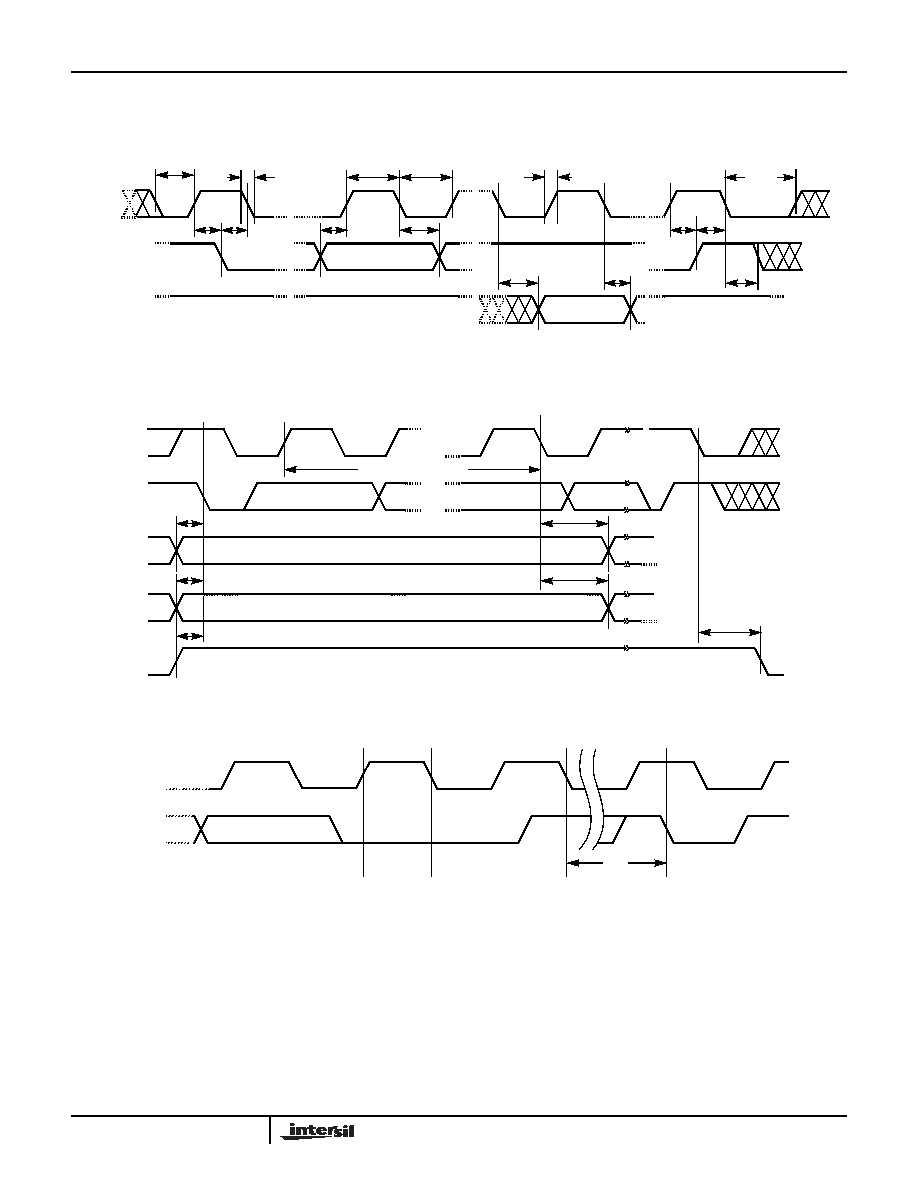
ViMON
ViGDO
V
REFi
t
TO
i = 1, 3, 4
Initial
Power-up
t
DELAYi
V
CC
t
DPOR
t
DELAYi
FIGURE 1. INITIAL POWER UP TIMING
ViGDO
MR
t
MR
t
DELAYi
t
MRE
RESET
t
DELAYi
+ t
SPOR
FIGURE 2. MANUAL RESET (MR)
t
DELAY1
V1GDO
t
DELAY3
V3GDO
t
DELAY4
V4GDO
t
SPOR
RESET
Any ViGDO
(1st occurance)
ViMON
MR
t
DELAY1
t
DELAY3
t
DELAY4
t
SPOR
(i= 1 to 4)
FIGURE 3. ViGDO, RESET TIMINGS
X80130, X80131, X80132, X80133, X80134

6
FN8152.0
January 20, 2005
Serial Interface
Over the recommended operating conditions unless otherwise specified.
SYMBOL
PARAMETER
TEST CONDITIONS
MIN
TYP
MAX
UNIT
DC CHARACTERISTICS
I
CC1
Active Supply Current (V
CC
) Read or Write
to Memory or CRs
V
IL
= V
CC
x 0.1
V
IH
= V
CC
x 0.9,
f
SCL
= 400kHz
2.5
mA
I
LI
Input Leakage Current (SCL, WP, A0, A1)
V
IL
= GND to V
CC
15
µA
I
LO
Output Leakage Current (SDA)
V
SDA
= GND to V
CC
Device is in Standby
15
µA
V
IL
Input LOW Voltage (SDA, SCL, WP, A0, A1)
-0.5
V
CC
x 0.3
V
V
IH
Input HIGH Voltage (SDA, SCL, WP, A0, A1)
V
CC
x 0.7
5.5
V
V
HYS
Schmitt Trigger Input Hysteresis
V
CC
related level
0.05 x 5
V
Fixed input level
0.2
V
V
OL
Output LOW Voltage (SDA)
I
OL
= 4.0mA
0.4
V
AC CHARACTERISTICS
f
SCL
SCL Clock Frequency
400
kHz
t
IN
Pulse width Suppression Time at inputs
50
ns
t
AA
(Note 1) SCL LOW to SDA Data Out Valid
0.1
1.5
µs
t
BUF
(Note 1)
Time the bus is free before start of new
transmission
1.3
µs
t
LOW
Clock LOW Time
1.3
µs
t
HIGH
Clock HIGH Time
0.6
µs
t
SU:STA
Start Condition Setup Time
0.6
µs
t
HD:STA
Start Condition Hold Time
0.6
µs
t
SU:DAT
Data In Setup Time
100
ns
t
HD:DAT
Data In Hold Time
0
µs
t
SU:STO
Stop Condition Setup Time
0.6
µs
t
DH
(Note 1) Data Output Hold Time
50
ns
t
R
(Note 1)
SDA and SCL Rise Time
20 +.1Cb
300
ns
t
F
(Note 1)
SDA and SCL Fall Time
20 +.1Cb
300
ns
t
SU:WP
WP Setup Time
0.6
µs
t
HD:WP
WP Hold Time
0
µs
t
SU:ADR
A0, A1 Setup Time
0.6
µs
t
HD:ADR
A0, A1 Hold Time
0
µs
t
SU:VP
V
P
Setup Time
0.6
µs
Cb
(Note 3) Capacitive load for each bus line
400
pF
t
WC
(Note 2) EEPROM Write Cycle Time
5
10
ms
NOTES:
1. This parameter is based on characterization data.
2. t
WC
is the time from a valid STOP condition at the end of a write sequence to the end of the self-timed internal nonvolatile write cycle. It is the
minimum cycle time to be allowed for any nonvolatile write by the user, unless Acknowledge Polling is used.
3. This parameter is not 100% tested.
X80130, X80131, X80132, X80133, X80134
7
FN8152.0
January 20, 2005
Timing Diagrams
t
SU:STO
t
HIGH
t
SU:STA
t
HD:STA
t
HD:DAT
t
SU:DAT
SCL
SDA IN
SDA OUT
t
F
t
LOW
t
HD:DAT
t
R
t
DH
t
AA
t
BUF
t
HD:STO
t
BUF
FIGURE 4. BUS TIMING
t
HD:WP
SCL
SDA IN
WP
t
SU:WP
Clk 1
Clk 9
Slave Address Byte
START
WP
V
P
t
SU:VP
t
WC
t
HD:ADR
t
SU:ADR
A1, A0
STOP
FIGURE 5. WP, A0, A1, VP PIN TIMING
SCL
SDA
t
WC
8
th
Bit of Last Byte
ACK
Stop
Condition
Start
Condition
FIGURE 6. WRITE CYCLE TIMING
X80130, X80131, X80132, X80133, X80134

8
FN8152.0
January 20, 2005
Symbol Table
Pinout
Must be
steady
Will be
steady
May change
from LOW
Will change
from LOW
to HIGH
May change
from HIGH
to LOW
Will change
from HIGH
to LOW
Don't Care:
Changes
Allowed
Changing:
State Not
Known
WAVEFORM INPUTS
OUTPUTS
to HIGH
QFN package
(Top view)
V1GDO
MR
NC
V3GDO
DNC
V4MON
V3MON
V1MON
RESET
WP
V4GDO
SCL
1
2
3
4
5
6
7
18
19
20
V
CC
8
17
(5mm x 5mm)
9 10
11
V
P
12
14
15
16
13
A0
DNC
A1
SD
A
V
CC
V
SS
Pin Descriptions
PIN
NAME
DESCRIPTION
1
V4GDO
V4 Voltage Good Delay Output (Active LOW). This open drain output goes HIGH when V4MON is less than V
REF4
and goes LOW when V4MON is greater than V
REF4
. There is user selectable delay circuitry on this pin.
2
V4MON
V4 Voltage Monitor Input. Third voltage monitor pin. If unused connect to V
CC
.
3
V3GDO
V3 Voltage Good Delay Output (Active LOW). This open drain output goes HIGH when V3MON is less than V
REF3
and goes LOW when V3MON is greater than V
REF3
. There is user selectable delay circuitry on this pin.
4
V3MON
V3 Voltage Monitor Input. Second voltage monitor pin. If unused connect to V
CC
.
5
DNC
Do Not Connect.
6
V
P
EEPROM programming Voltage.
7
V
CC
Connect to V
CC
.
8
DNC
Do Not Connect.
9
A1
Address Select Input. It has an internal pull-down resistor. (>10M
typical)
The A0 and A1 bits allow for up to 4 X80130 devices to be used on the same SMBus serial interface.
10
SDA
Serial Data. SDA is a bidirectional pin used to transfer data into and out of the device.
It has an open drain output and may be wire ORed with other open drain or open collector outputs. This pin requires
a pull up resistor and the input buffer is always active (not gated).
11
SCL
Serial Clock. The Serial Clock controls the serial bus timing for data input and output.
12
V1MON
V1 Voltage Monitor Input. First voltage monitor pin. If unused connect to V
CC
.
13
V1GDO
V1 Voltage Good Delay Output (Active LOW). This open drain output goes HIGH when V1MON is less than V
REF1
and goes LOW when V1MON is greater than V
REF1
. There is user selectable delay circuitry on this pin.
14
RESET
RESET Output. This open drain pin is an active LOW output. This pin will be active until all ViGDO pins go inactive
and the power sequencing is complete. This pin will be released after a programmable delay.
15
WP
Write Protect. Input Pin. WP HIGH (in conjunction with WPEN bit=1) prevents writes to any memory location in the
device. It has an internal pull-down resistor. (>10M
typical)
16
MR
Manual Reset. Pulling the MR pin HIGH initiates a RESET. The MR signal must be held HIGH for 5
µsecs. It has an
internal pull-down resistor. (>10M
typical)
17
V
SS
Ground Input.
18
NC
No Connect. No internal connections.
19
A0
Address Select Input. It has an internal pull-down resistor. (>10M
typical)
The A0 and A1 bits allow for up to 4 X80130 devices to be used on the same SMBus serial interface.
20
V
CC
Supply Voltage.
X80130, X80131, X80132, X80133, X80134
9
FN8152.0
January 20, 2005
Description
The X80130 is a voltage supervisor/sequencer with three
built in voltage monitors. This allows the designer to monitor
up to three voltages and sequence up to four events.
Low voltage detection circuitry protects the system from
power supply failure or "brown out" conditions, resetting the
system and resequencing the voltages when any of the
monitored inputs fall below the minimum threshold level. The
RESET pin is active until all monitored voltages reach proper
operating levels and stabilize for a selectable period of time.
Five common low voltage combinations are available,
however, Intersil's unique circuits allow the any voltage
monitor threshold to be reprogrammed for special needs or
for applications requiring higher precision.
A manual reset input provides debounce circuitry for
minimum reset component count. Activating the manual
reset both controls the RESET output and resequences the
supplies through control of the ViGDO pins.
The X80130 has 2kb of EEPROM for system configuration,
manufacturing or maintenance information. This memory is
protected to prevent inadvertent changes to the contents.
Functional Description
Power On Reset and System Reset With Delay
Application of power to the X80130 activates a Power On
Reset circuit that pulls the RESET pin active. This signal, if
used, prevents the system microprocessor from starting to
operate while there is insufficient voltage on any of the
supplies. This circuit also does the following:
∑ It prevents the processor from operating prior to
stabilization of the oscillator.
∑ It allows time for an FPGA to download its configuration
prior to initialization of the circuit.
∑ It prevents communication to the EEPROM during
unstable power conditions, greatly reducing the likelihood
of data corruption on power up.
∑ It allows time for all supplies to turn on and stabilize prior
to system initialization.
The POR/RESET circuit is activated when all voltages are
within specified ranges and the V1GDO, V3GDO, and
V4GDO time-out conditions are met. The POR/RESET
circuit will then wait t
SPOR
and de-assert the RESET pin.
The POR delay may be changed by setting the TPOR bits in
register CR2. The delay can be set to 100ms, 500ms, 1
second, or 5 seconds.
Manual Reset
The manual reset option allows a hardware reset of the
power sequencing pins. These can be used to recover the
system in the event of an abnormal operating condition.
Activating the MR pin for more than 5
µs sets all of the
ViGDO outputs and the RESET output active (LOW). When
MR is released (and if all supplies are still at their proper
operating voltage) then the ViGDO and RESET pins will be
released after their programmed delay periods.
Triple Voltage Monitoring
X80130 monitors 3 voltage inputs. When the ViMON (i =1, 3,
4) input is detected to be above the input threshold, the
output ViGDO (i =1, 3, 4) goes inactive (LOW). The ViGDO
signal is de-asserted after a delay of 100ms. This delay can
be changed on each ViGDO output individually with bits in
register CR3. The delay can be 100ms, 500ms, 1s and 5s.
Each ViGDO signal remains active until its associated
ViMON input rises above the threshold.
Fault Detection
The X80130 contains a Fault Detection Register (FDR) that
provides the user the status of the causes for a RESET pin
active (See Table 20).
At power-up, the FDR is defaulted to all "0". The system
needs to initialize the register to 0Dh before the actual
monitoring can take place. In the event that any one of the
monitored sources fail, the corresponding bit in the register
changes from a "1" to a "0" to indicate the failure. When a
RESET is detected by the main controller, the controller
should read the FDR and note the cause of the fault. After
reading the register, the controller can reset the register bit
back to all "1" in preparation for future failure conditions.
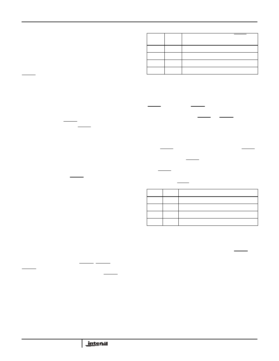
TABLE 1. POR RESET DELAY OPTIONS
TPOR1
TPOR0
t
SPOR
DELAY BEFORE RESET
ASSERTION
0
0
100 miliseconds (default)
0
1
500 miliseconds
1
0
1 second
1
1
5 seconds
TABLE 2. ViGDO OUTPUT TIME DELAY OPTIONS
TiD1
TiD0
t
DELAYi
0
0
100ms (default)
0
1
500ms
1
0
1 secs
1
1
5 secs
where i is the specific voltage monitor (i = 1, 3, 4).
X80130, X80131, X80132, X80133, X80134

10
FN8152.0
January 20, 2005
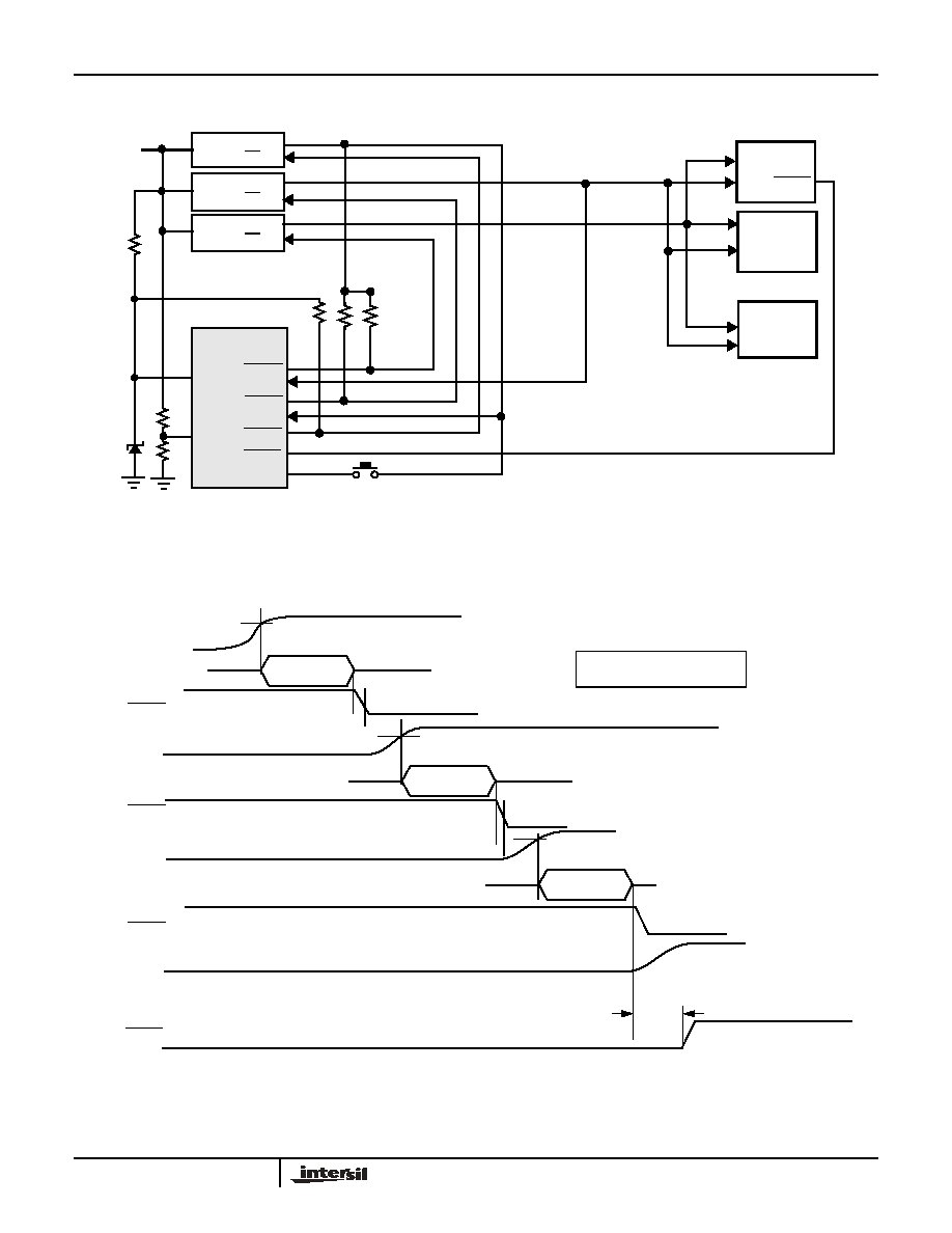
Flexible Power Sequencing of Multiple Power
Supplies
The X80130 provides several circuits such as multiple
voltage monitors, programmable delays, and output drive
signals that can be used to set up flexible power monitoring
or sequencing schemes system power supplies. Below are
two examples:
1. Power Up of Supplies In Parallel Using Programmable
Delays (See Figure 7 and Figure 8).
The X80130 monitors several power supplies, powered
by the same source voltage, that all begin power up at the
same time. Each voltage source is fed into the ViMON
inputs to the X80130. The ViMON inputs monitor the
voltage to make sure it has reached the minimum desired
level. When each voltage monitor determines that its
input is good, a counter starts. After the programmed
delay time, the X80130 sets the ViGDO signals LOW. The
ViGDO signals can be wire ORed together and tied to an
interrupt on the microcontroller. Any individual voltage
failure can be viewed in the Fault Detection Register.
In the factory default condition, each ViGDO output is
instructed to go LOW 100ms after the input voltage
reaches its threshold. However, each ViGDO delay is
individually selectable as 100ms, 500ms, 1s and 5s. The
delay times are charged via the SMBus during calibration
of the system.
2. Power Up of Supplies Via Relay Sequencing Using
Voltage Monitors (See Figure 9 and Figure 10).
Several power supplies and their respective power up
start times can be controlled using the X80130 such that
each of the power supplies will start in a relay sequencing
fashion. In the following example, the 1st supply is
allowed to power up when the input regulated supply
reaches an acceptable threshold. Subsequent supplies
power up after the prior supply has reached its operating
voltage. This configuration ensures that each subsequent
power supply turns on after the preceding supplies
voltage output is valid. Again, the X80130 offers
programmable delays for each voltage monitor and this
delay is selectable via the SMBus during calibration of the
system.
V4GDO
V4MON
V3GDO
V3MON
V1GDO
V1MON
X80130/31/32/33/34
RESET
µC
V
CC1
FPGA
V
CC1
ASIC
V
CC1
RESET
V
CC2
V
CC2
V
CC2
MR
1.2V
2.5V
3.3V
5V
Power
Supplies
IRQ
On/Off
On/Off
On/Off
FIGURE 7. EXAMPLE APPLICATION OF PARALLEL
POWER CONTROL
V1MON
t
DELAY1
V1GDO
Programmable
Delay
Timing
not to scale
100ms
500ms
1sec
5secs
V3MON
t
DELAY3
V3GDO
Programmable
Delay
V4MON
t
DELAY4
V4GDO
Programmable
Delay
t
SPOR
Programmable
Delay
RESET
Can Choose Different
Delays for each
Voltage Monitor
FIGURE 8. PARALLEL POWER CONTROL - TIMING
X80130, X80131, X80132, X80133, X80134
11
FN8152.0
January 20, 2005
X80140/41/42/43
RESET
µC
V
CC1
FPGA
V
CC1
ASIC
V
CC1
V
CC2
V
CC2
V
CC2
On/Off
5V
Power
Supply
On/Off
1.2V
Power
Supply
On/Off
3.3V
Power
Supply
12V
V4GDO
V4MON
V3GDO
V3MON
V1GDO
V1MON
RESET
MR
5V
V
CC
FIGURE 9. EXAMPLE OF RELAY POWER SUPPLY SEQUENCING
V1MON
t
DELAY1
V1GDO
V1MON
threshold
Power Supply
#2 ON
Power Supply
V2MON
threshold
Power Supply
#4 ON
V3GDO
Timing Not
To Scale
Example: Four Independent
Power Supplies in relay timing
100ms
V4GDO
Programmable
Delay
Programmable
Delay
#2 OUTPUT
500ms
1sec
5sec
100ms
500ms
1sec
5sec
t
DELAY3
Power Supply
#3 ON
V3MON
threshold
100ms
500ms
1sec
5sec
t
DELAY4
Programmable
Delay
Power Supply
#3 OUTPUT
Power Supply
#4 OUTPUT
(12V)
(5V)
(1.2V)
(3.3V)
t
SPOR
RESET
FIGURE 10. RELAY SEQUENCING OF DC-DC SUPPLIES (TIMING)
X80130, X80131, X80132, X80133, X80134

12
FN8152.0
January 20, 2005
Control Registers and Memory
The user addressable internal control, status and memory
components of the X80130 can be split up into three parts:
∑ Control Register (CR)
∑ Fault Detection Register (FDR)
∑ EEPROM array
Registers
The Control Registers and Fault Detection Register are
summarized in Table 4. Changing bits in these registers
change the operation of the device or clear fault conditions.
Reading bits from these registers provides information about
device configuration or fault conditions. Reads and writes
are done through the SMBus serial port.
All of the Control Register bits are nonvolatile (except for the
WEL bit), so they do not change when power is removed.
The values of the Register Block can be read at any time by
performing a random read (See Serial Interface) at the
specific byte address location. Only one byte is read by each
register read operation.
Bits in the registers can be modified by performing a single
byte write operation directly to the address of the register
and only one data byte can change for each register write
operation.
The X80130 contains a 2kbit EEPROM memory array. This
array can contain information about manufacturing location
and dates, board configuration, fault conditions, service
history, etc. Access to this memory is through the SMBus
serial port. Read and write operations are similar to those of
the control registers, but a single command can write up to
16 bytes at one time. A single read command can return the
entire contents of the EEPROM memory.
Register and Memory Protection
In order to reduce the possibility of inadvertent changes to
either a control register of the contents of memory, several
protection mechanisms are built into the X80130. These are
a Write Enable Latch, Block Protect bits, a Write Protect
Enable bit and a Write Protect pin.
WEL: Write Enable Latch
A write enable latch (WEL) bit controls write accesses to the
nonvolatile registers and the EEPROM memory array in the
X80130. This bit is a volatile latch that powers up in the LOW
(disabled) state. While the WEL bit is LOW, writes to any
address (registers or memory) will be ignored. The WEL bit
is set by writing a "1" to the WEL bit and zeroes to the other
bits of the control register 0 (CR0). It is important to write
only 00h or 80h to the CR0 register.
Once set, WEL remains set until either it is reset to 0 (by
writing a "0" to the WEL bit and zeroes to the other bits of the
control register) or until the part powers up again.
Note, a write to FDR or RSR does not require that WEL=1.
BP1 and BP0: Block Protect Bits
The Block Protect Bits, BP1 and BP0, determine which
blocks of the memory array are write protected. A write to a
protected block of memory is ignored. The block protect bits
will prevent write operations to one of four segments of the
array.
WPEN: Write Protect Enable
The Write Protect pin and Write Protect Enable bit in the
CR1 register control the Programmable Hardware Write
Protect feature. Hardware Protection is enabled when the
WP pin is HIGH and WPEN bit is HIGH and disabled when
WP pin is LOW or the WPEN bit is LOW. When the chip is
Hardware Write Protected, non-volatile writes to all control
registers (CR1, CR2 and CR3) are disabled including BP
bits, the WPEN bit itself, and the blocked sections in the
memory Array. Only the section of the memory array that are
not block protected can be written.
Non Volatile Programming Voltage (V
P
)
Nonvolatile writes require that a programming voltage be
applied to the VP for the duration of a nonvolatile write
operation.
BP1
BP0
PROTECTED ADDRESSES
(SIZE)
ARRAY LOCK
0
0
None (Default)
None (Default)
0
1
C0h - FFh (64 bytes)
Upper 1/4
1
0
80h - FFh (128 bytes)
Upper 1/2
1
1
00h - FFh (256 bytes)
All
TABLE 3. WRITE PROTECT CONDITIONS
WEL
WP
WPEN
MEMORY ARRAY
NOT BLOCK
PROTECTED
MEMORY ARRAY
BLOCK PROTECTED
WRITES TO
CR1, CR2, CR3
PROTECTION
LOW
X
X
Writes Blocked
Writes Blocked
Writes Blocked
Hardware
HIGH
LOW
X
Writes Enabled
Writes Blocked
Writes Enabled
Software
HIGH
X
LOW
Writes Enabled
Writes Blocked
Writes Enabled
Software
HIGH
HIGH
HIGH
Writes Enabled
Writes Blocked
Writes Blocked
Hardware
X80130, X80131, X80132, X80133, X80134
13
FN8152.0
January 20, 2005
Bus Interface Information
Interface Conventions
The device supports a bidirectional bus oriented protocol.
The protocol defines any device that sends data onto the
bus as a transmitter, and the receiving device as the
receiver. The device controlling the transfer is called the
master and the device being controlled is called the slave.
The master always initiates data transfers, and provides the
clock for both transmit and receive operations. Therefore,
the devices in this family operate as slaves in all
applications.
It should be noted that the ninth clock cycle of the read
operation is not a "don't care." To terminate a read operation,
the master must either issue a STOP condition during the
ninth cycle or hold SDA HIGH during the ninth clock cycle
and then issue a STOP condition.
Serial Clock and Data
Data states on the SDA line can change only during SCL
LOW. SDA state changes during SCL HIGH are reserved for
indicating START and STOP conditions (See Figure 11).
Serial Start Condition
All commands are preceded by the START condition, which
is a HIGH to LOW transition of SDA when SCL is HIGH. The
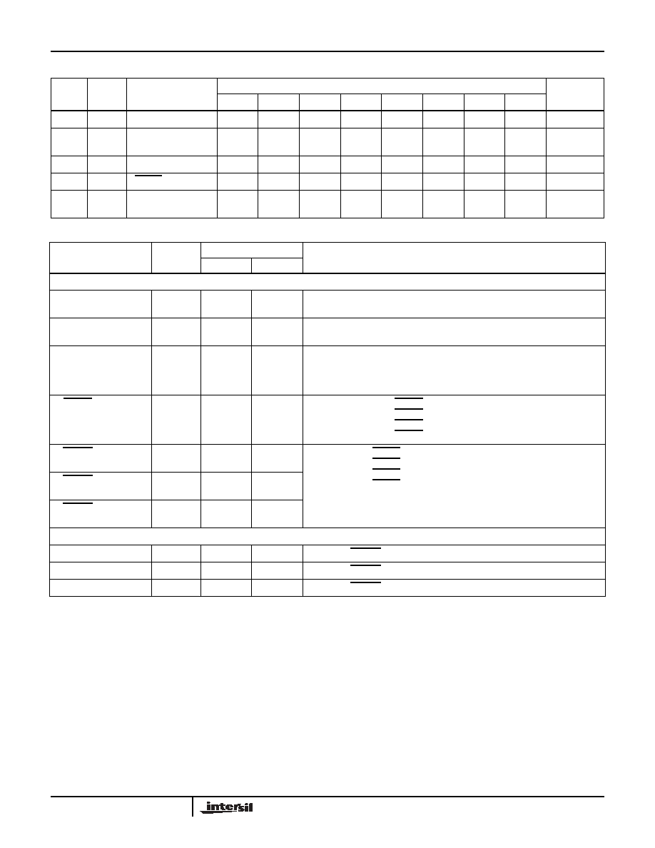
TABLE 4. REGISTER ADDRESS MAP
BYTE
ADDR.
NAME
CONTROI/STATUS
BIT
MEMORY
TYPE
7
6
5
4
3
2
1
0
00H
CR0
Write Enable
WEL
0
0
0
0
0
0
0
Volatile
01H
CR1
EEPROM Block
Control
WPEN
0
0
BP1
BP0
0
0
0
EEPROM
02H
CR2
POR Timing
0
0
0
0
TPOR1
TPOR0
0
0
EEPROM
03H
CR3
ViGDO TIme Delay
T4D1
T4D0
T3D1
T3D0
0
0
T1D1
T1D0
EEPROM
FF
FDR
Fault Detection
Register
0
0
0
0
V40S
V30S
0
V10S
Volatile
TABLE 5. HARDWARE/SOFTWARE CONTROL AND FAULT DETECTION BITS SUMMARY
OPERATION
CONTROL
/STATUS
LOCATION(S)
DESCRIPTION (SEE FUNCTIONAL FOR DETAILS)
REGISTER
BITS
SOFTWARE CONTROL BITS
EEPROM Write Enable
WEL
CR0
7
WEL = 1 enables write operations to the control registers and EEPROM.
WEL = 0 prevents write operations.
EEPROM Write Protect
WPEN
CR1
7
WPEN = 1 (and WP pin HIGH) prevents writes to the control registers and the
EEPROM.
EEPROM Block Protect
BP1
BP0
CR1
4:3
BP1=0, BP0=0 : No EEPROM memory protected.
BP1=0, BP0=1 : Upper 1/4 of EEPROM memory protected
BP1=1, BP0=0 : Upper 1/2 of EEPROM memory protected.
BP1=1, BP0=1 : All of EEPROM memory protected.
RESET Time Delay
TPOR0
TPOR1
CR2
3:2
TPOR1=0, TPOR0=0 : RESET delay = 100ms
TPOR1=0, TPOR0=1 : RESET delay = 500ms
TPOR1=1, TPOR0=0 : RESET delay = 1s
TPOR1=1, TPOR0=1 : RESET delay = 5s
V1GDO Time Delay
T1D0
T1D1
CR3
1:0
TiD1=0, TiD0=0 : ViGDO delay = 100ms
TiD1=0, TiD0=1 : ViGDO delay = 500ms
TiD1=1, TiD0=0 : ViGDO delay = 1s
TiD1=1, TiD0=1 : ViGDO delay = 5s
V3GDO Time Delay
T3D0
T3D1
CR3
5:4
V4GDO Time Delay
T4D0
T4D1
CR3
7:6
STATUS BITS
1st Voltage Monitor
V1OS
FDR
0
V1OS = 0 : V1GDO pin has been asserted (must be preset to 1).
3rd Voltage Monitor
V3OS
FDR
2
V3OS = 0 : V3GDO pin has been asserted (must be preset to 1).
4th Voltage Monitor
V4OS
FDR
3
V4OS = 0 : V4GDO pin has been asserted (must be preset to 1).
X80130, X80131, X80132, X80133, X80134

14
FN8152.0
January 20, 2005
device continuously monitors the SDA and SCL lines for the
START condition and does not respond to any command
until this condition has been met. On power up, the SCL pin
must be brought LOW prior to the START condition.
Serial Stop Condition
All communications must be terminated by a STOP
condition, which is a LOW to HIGH transition of SDA when
SCL is HIGH, followed by a HIGH to LOW on SCL. After
going LOW, SCL can stay LOW or return HIGH. The STOP
condition also places the device into the Standby power
mode after a read sequence.
Serial Acknowledge
Acknowledge is a software convention used to indicate
successful data transfer. The transmitting device, either
master or slave, will release the bus after transmitting eight
bits. During the ninth clock cycle, the receiver will pull the
SDA line LOW to acknowledge that it received the eight bits
of data (See Figure 12).
The device will respond with an acknowledge after
recognition of a START condition and if the correct Device
Identifier and Select bits are contained in the Slave Address
Byte. If a write operation is selected, the device will respond
with an acknowledge after the receipt of each subsequent
eight bit word. The device will acknowledge all incoming data
and address bytes, except for the Slave Address Byte when
the Device Identifier and/or Select bits are incorrect.
The device does not acknowledge any instructions following
a non-volatile write operation, unless the V
P
pin has the
recommended programming voltage applied for the duration
of the write cycle.
In the read mode, the device will transmit eight bits of data,
release the SDA line, then monitor the line for an
acknowledge. If an acknowledge is detected and no STOP
condition is generated by the master, the device will continue
to transmit data. The device will terminate further data
transmissions if an acknowledge is not detected. The master
must then issue a STOP condition to return the device to
Standby mode and place the device into a known state.
Device Addressing
Addressing Protocol Overview
Depending upon the operation to be performed on each of
these individual parts, a 1, 2 or 3 Byte protocol is used. All
operations however must begin with the Slave Address Byte
being clocked into the SMBus port on the SCL and SDA
pins. The Slave address selects the part of the device to be
addressed, and specifies if a Read or Write operation is to
be performed.
Slave Address Byte
Following a START condition, the master must output a
Slave Address Byte. This byte consists of three parts:
∑ The Device Type Identifier which consists of the most
significant four bits of the Slave Address (SA7 - SA4). The
Device Type Identifier MUST be set to 1010 in order to
select the device.
∑ The next two bits (SA3 - SA2) are slave address bits. The
bits received via the SMBus are compared to A0 and A1
pins and must match or the communication is aborted.
The next bit, SA1, selects the device memory sector.
There are two addressable sectors: the memory array and
the control, fault detection and remote shutdown registers.
∑ The Least Significant Bit of the Slave Address (SA0) Byte
is the R/W bit. This bit defines the operation to be
performed. When the R/W bit is "1", then a READ
operation is selected. A "0" selects a WRITE operation
(Refer to Figure 13).
SCL
SDA
Start
Stop
FIGURE 11. VALID START AND STOP CONDITIONS
Data Output from
Transmitter
Data Output from
Receiver
8
1
9
Start
Acknowledge
SCL from
Master
FIGURE 12. ACKNOWLEDGE RESPONSE FROM RECEIVER
X80130, X80131, X80132, X80133, X80134

15
FN8152.0
January 20, 2005
Serial Write Operations
Before any write operations can be performed, a
programming supply voltage (V
P
) must be supplied. This
voltage is only needed for programming, but the nonvolatile
registers and EEPROM locations cannot be programmed
without it.
In order to successfully complete a write operation to either a
Control Register or the EEPROM array, the Write Enable
Latch (WEL) bit must first be set and either the WP pin or the
WPEN bit must be LOW.
Writes to the WEL bit do not cause a high voltage write
cycle, so the device is ready for the next operation
immediately after the STOP condition.
BYTE WRITE
For a write operation, the device requires the Slave Address
Byte and a Word Address Byte. This gives the master
access to any one of the words in the array. After receipt of
the Word Address Byte, the device responds with an
acknowledge, and awaits the next eight bits of data. After
receiving the 8 bits of the Data Byte, the device again
responds with an acknowledge. The master then terminates
the transfer by generating a STOP condition, at which time
the device begins the internal write cycle to the nonvolatile
memory. During this internal write cycle, the device inputs
are disabled, so the device will not respond to any requests
from the master. The SDA output is at high impedance.
A write to a protected block of memory will suppress the
acknowledge bit.
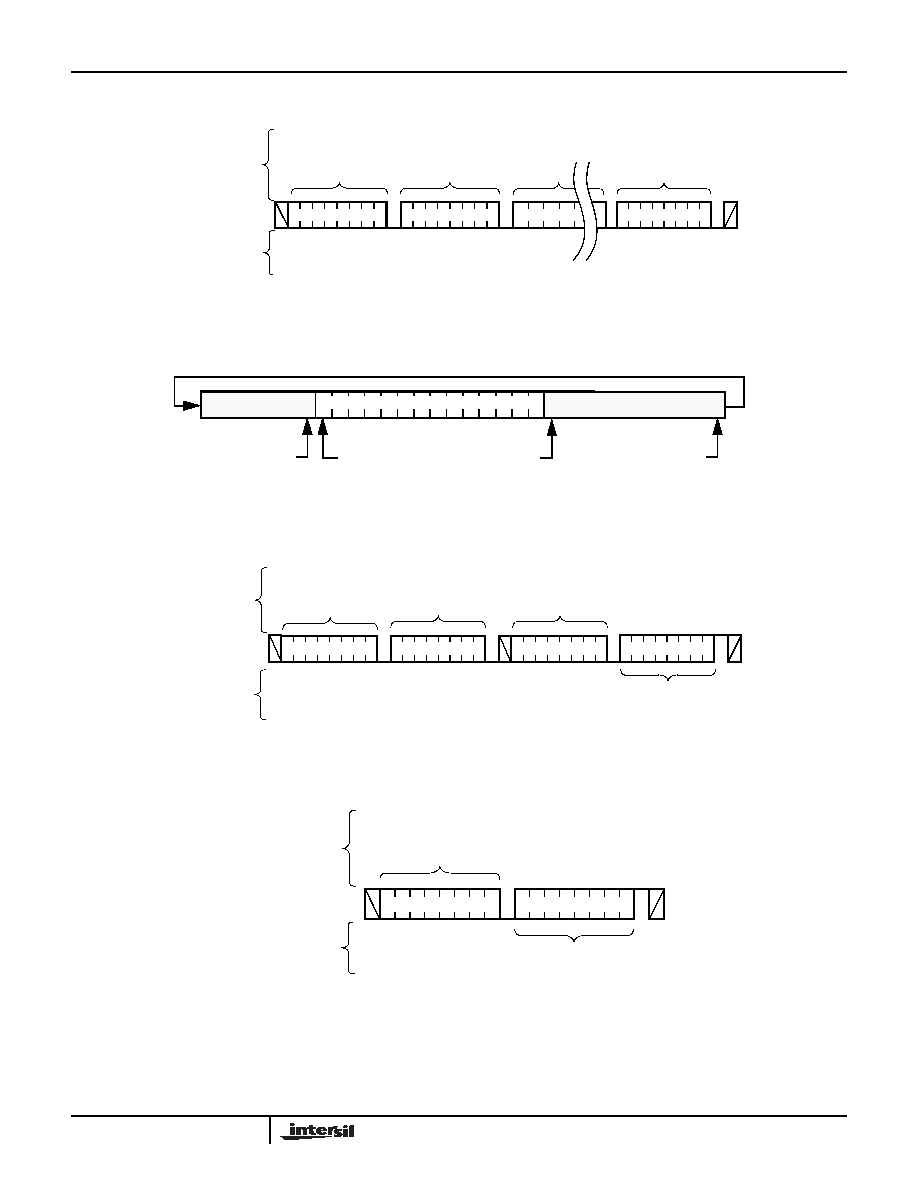
PAGE WRITE
The device is capable of a page write operation (See Figure
14). It is initiated in the same manner as the byte write
operation; but instead of terminating the write cycle after the
first data byte is transferred, the master can transmit an
unlimited number of 8-bit bytes. After the receipt of each
byte, the device will respond with an acknowledge, and the
address is internally incremented by one. The page address
remains constant. When the counter reaches the end of the
page, it "rolls over" and goes back to `0' on the same page
(See Figure 15).
This means that the master can write 16 bytes to the page
starting at any location on that page. If the master begins
writing at location 10, and loads 12 bytes, then the first 6
bytes are written to locations 10 through 15, and the last 6
bytes are written to locations 0 through 5. Afterwards, the
address counter would point to location 6 of the page that
was just written. If the master supplies more than 16 bytes of
data, then new data overwrites the previous data, one byte
at a time.
The master terminates the Data Byte loading by issuing a
STOP condition, which causes the device to begin the
nonvolatile write cycle. As with the byte write operation, all
inputs are disabled until completion of the internal write
cycle.
STOPS AND WRITE MODES
Stop conditions that terminate write operations must be sent
by the master after sending at least 1 full data byte plus the
subsequent ACK signal. If a STOP is issued in the middle of
a data byte, or before 1 full data byte plus its associated ACK
is sent, then the device will reset itself without performing the
write. The contents of the array will not be affected.
ACKNOWLEDGE POLLING
The disabling of the inputs during high voltage cycles can be
used to take advantage of the typical 5ms write cycle time.
Once the STOP condition is issued to indicate the end of the
master's byte load operation, the device initiates the internal
high voltage cycle. Acknowledge polling can be initiated
immediately. To do this, the master issues a START
condition followed by the Slave Address Byte for a write or
read operation. If the device is still busy with the high voltage
cycle then no ACK will be returned. If the device has
completed the write operation, an ACK will be returned and
the host can then proceed with the read or write operation
(See Figure 18).
SA6
SA7
SA5
SA3
SA2
SA1
SA0
Device Type Identifier
READ /
SA4
R/W
1
0
1
0
WRITE
Address
External
Device
Memory
Select
A1
A0
MS
INTERNAL
ADDRESS (SA1)
INTERNALLY ADDRESSED
DEVICE
0
EEPROM Array
1
Control Register,
Fault Detection Register
BIT SA0
OPERATION
0
WRITE
1
READ
FIGURE 13. SLAVE ADDRESS FORMAT
X80130, X80131, X80132, X80133, X80134
16
FN8152.0
January 20, 2005
S
t
a
r
t
S
t
o
p
Slave
Address
Byte
Address
Data
(n)
A
C
K
A
C
K
A
C
K
SDA Bus
Signals from
the Slave
Signals from
the Master
0
Data
(1)
A
C
K
(1 to n to 16)
1 0 1 0
FIGURE 14. PAGE WRITE OPERATION
address
address
10
5 Bytes
n-1
7 Bytes
address
= 6
address pointer
ends here
Addr = 7
FIGURE 15. WRITING 12 BYTES TO A 16-BYTE PAGE STARTING AT LOCATION 10
0
Slave
Address
Byte
Address
A
C
K
A
C
K
S
t
a
r
t
S
t
o
p
Slave
Address
Data
A
C
K
1
S
t
a
r
t
SDA Bus
Signals from
the Slave
Signals from
the Master
1 0 1 0
1 0 1 0
FIGURE 16. RANDOM ADDRESS READ SEQUENCE
S
t
a
r
t
S
t
o
p
Slave Address
Data
SDA Bus
Signals from
the Slave
Signals from
the Master
1
A
C
K
1 0 1
0
FIGURE 17. CURRENT ADDRESS READ SEQUENCE
X80130, X80131, X80132, X80133, X80134

17
FN8152.0
January 20, 2005
Serial Read Operations
Read operations are initiated in the same manner as write
operations with the exception that the R/W bit of the Slave
Address Byte is set to one. There are three basic read
operations: Current Address Reads, Random Reads, and
Sequential Reads.
RANDOM READ
Random read operation allows the master to access any
memory location in the array. Prior to issuing the Slave
Address Byte with the R/W bit set to one, the master must
first perform a "dummy" write operation. The master issues
the START condition and the Slave Address Byte, receives
an acknowledge, then issues the Word Address Bytes. After
acknowledging receipts of the Word Address Bytes, the
master immediately issues another START condition and the
Slave Address Byte with the R/W bit set to one. This is
followed by an acknowledge from the device and then by the
eight bit word. The master terminates the read operation by
not responding with an acknowledge and then issuing a
STOP condition (See Figure 16 for the address,
acknowledge, and data transfer sequence).
CURRENT ADDRESS READ
Internally the device contains an address counter that
maintains the address of the last word read incremented by
one. Therefore, if the last read was to address n, the next
read operation would access data from address n+1. On
power up, the address of the address counter is undefined,
requiring a read or write operation for initialization.
Upon receipt of the Slave Address Byte with the R/W bit set
to one, the device issues an acknowledge and then
transmits the eight bits of the Data Byte. The master
terminates the read operation when it does not respond with
an acknowledge during the ninth clock and then issues a
STOP condition (See Figure 17 or the address,
acknowledge, and data transfer sequence).
Operational Notes
The device powers-up in the following state:
∑ The device is in the low power standby state.
∑ The WEL bit is set to `0'. In this state it is not possible to
write to the device.
∑ SDA pin is the input mode.
Data Protection
The following circuitry has been included to prevent
inadvertent writes:
∑ The WEL bit must be set to allow write operations.
∑ The proper clock count and bit sequence is required prior
to the STOP bit in order to start a nonvolatile write cycle.
∑ The WP pin, when held HIGH, prevents all writes to the
array and all the Register.
∑ A programming voltage must be applied to the V
P
pin prior
to any programming sequence.
ACK
Returned?
Issue Slave Address
Byte (Read or Write)
Byte Load Completed by
Issuing STOP.
Enter ACK Polling
Issue STOP
Issue START
NO
YES
High Voltage Cycle
Complete. Continue
Command Sequence?
Issue STOP
NO
Continue Normal Read
or Write Command
Sequence
PROCEED
YES
FIGURE 18. ACKNOWLEDGE POLLING SEQUENCE
X80130, X80131, X80132, X80133, X80134

18
All Intersil U.S. products are manufactured, assembled and tested utilizing ISO9000 quality systems.
Intersil Corporation's quality certifications can be viewed at www.intersil.com/design/quality
Intersil products are sold by description only. Intersil Corporation reserves the right to make changes in circuit design, software and/or specifications at any time without
notice. Accordingly, the reader is cautioned to verify that data sheets are current before placing orders. Information furnished by Intersil is believed to be accurate and
reliable. However, no responsibility is assumed by Intersil or its subsidiaries for its use; nor for any infringements of patents or other rights of third parties which may result
from its use. No license is granted by implication or otherwise under any patent or patent rights of Intersil or its subsidiaries.
For information regarding Intersil Corporation and its products, see www.intersil.com
FN8152.0
January 20, 2005
Packaging Information
20-Lead Quad Flat No Lead Package (Package Code: Q20)
5mm x 5mm Body with 0.65mm Lead Pitch
Note:
1. The package outline drawing is compati-
ble with JEDEC MO-220; variations:
WHHC-2, except dimensions D2 and E2.
2.
The terminal #1 identifier is a laser
marked feature
SYMBOLS
DIMENSIONS IN MILLIMETERS
MIN
NOM
MAX
A
0.70
0.75
0.80
A1
0.00
0.02
0.05
b
0.25
0.30
0.35
A3
0.19
0.20
0.25
D
4.90
5.00
5.10
D2
3.70
3.80
3.90
E
4.90
5.00
5.10
E2
3.70
3.80
3.90
e
--
0.65
--
L
0.35
0.40
0.45
y
--
0.08
Pin 1 Indent
E
D
A
A1
E2
D2
b
e
A3
L
C
y C
X80130, X80131, X80132, X80133, X80134