1
Æ
FN8154.0
CAUTION: These devices are sensitive to electrostatic discharge; follow proper IC Handling Procedures.
1-888-INTERSIL or 321-724-7143
|
Intersil (and design) is a registered trademark of Intersil Americas Inc.
Copyright Intersil Americas Inc. 2005. All Rights Reserved
All other trademarks mentioned are the property of their respective owners.
X80200, X80201, X80202, X80203, X80204
Power Supply Sequencer with Power-up
System Monitoring
The X80200 power sequencer provides a flexible approach
for handling difficult system power-up conditions. The
X80200 includes control of up to three voltage supplies and
can be cascaded to control additional supplies. The device
contains independent undervoltage lockout for each
controlled voltage.
The three voltage control circuits allow sequencing for
primary, core, and I/O voltages. The core and I/O supplies
are linked together with a comparator or a timer allowing a
tight coupling between these two supplies. The sequencing
may be either voltage based or time based.
The X80200 contains separate charge pumps to control
external N-channel power FETs for each of the supplies. The
charge pumps provide the high gate control voltage
necessary for efficient operation of the FET switches.
The X80200 turns on the primary voltage to the system
when the voltage source is steady. This primary FET switch
turn-on can be delayed with an external RC circuit. For the
secondary voltage sources, the device has a built-in "core-
up-first and core-down-last" sequencing logic which is ideal
for high performance processors, DSPs and ASICs.
The serial bus can be used to monitor the status or turn off
each of the external power switches. The X80200 has 3
slave address bits that allow up to 8 devices to be connected
to the same bus.
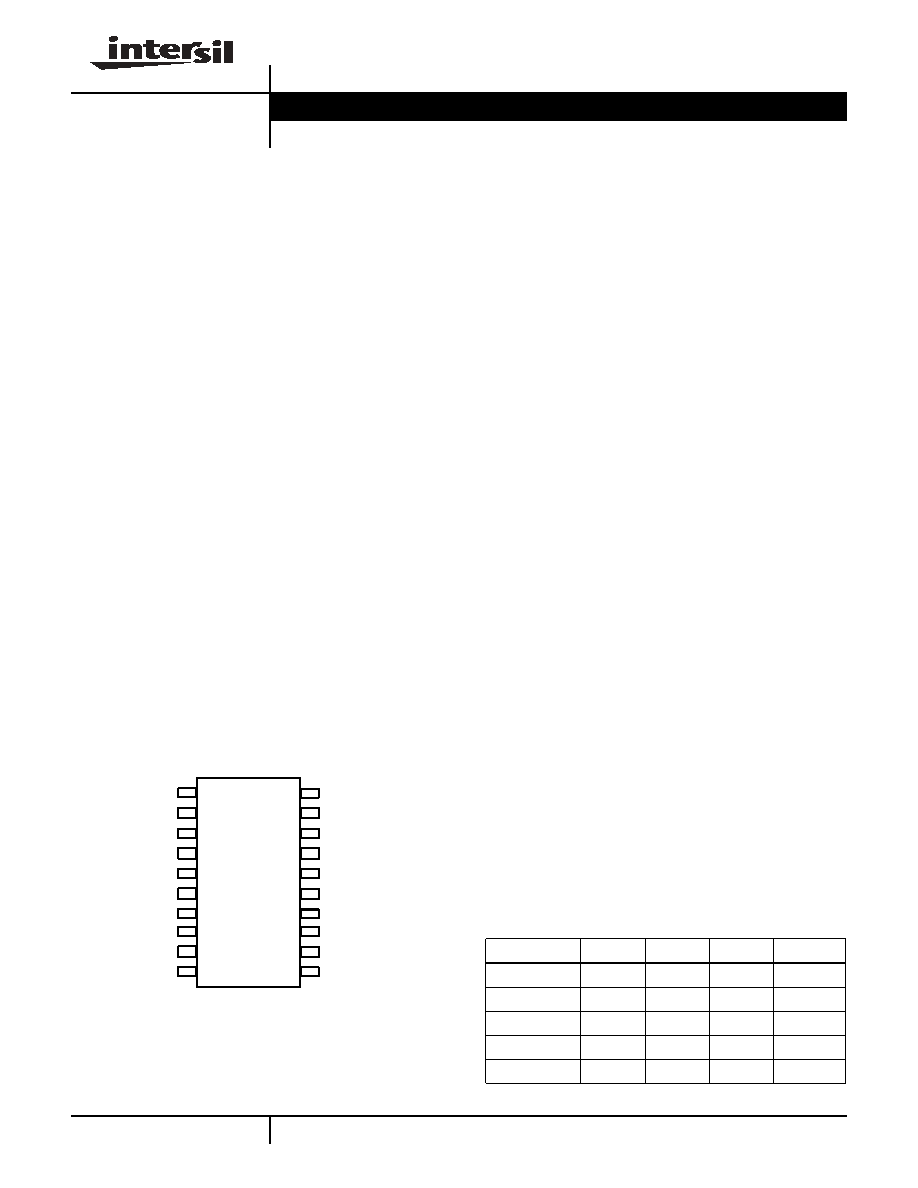
Pinout
20 LD TSSOP
TOP VIEW
Features
∑ Sequence three voltage supplies independently
- Core and Logic I/O VCC power sequencer for processor
supplies
- Power up and power down control
- Voltage monitors have undervoltage lockout
- Internal charge pump drives external N-channel FET
switches
- Cascadable to sequence more than 3 supplies
- Time based or voltage based sequencing
∑ Status register bits monitor gate output status
∑ SMBus compatible Interface
∑ Slave address identification for up to 8 power sequencers
(24 supplies) on the same bus
∑ Surface mount 20-pin TSSOP Package
Applications
∑ Distributed Power Supply Designs
∑ Multi-voltage systems
∑ Multiprocessor systems
∑ Embedded Processor Applications
∑ Digital Signal Processors, FPGAs, ASICs, Memory
Controllers
∑ N + 1 Redundant Power Supplies
∑ Support for SSI ≠ Server System Infrastructure
Specifications
∑ -48V Hotswap Power Backplane/Distribution
∑ Card Insertion Detection and Power
∑ Power Sequencing DC-DC Supplies
∑ Databus Power Interfacing
∑ Custom Industrial Power Backplanes
∑ Other: ATE, Data Acquisition, Mass Storage, Servers,
Data com, Wireless Basestations
VFB
GND
DNC
1
2
3
4
5
6
7
16
15
14
13
12
11
SETV
VDDL
REF
A0
A2
A1
VDDM
VDDH
GATE_H
GATEH_EN
READY
GATE_M
SCL
SDA
GATE_L
ENS
NC
8
9
10
20
19
18
17
Ordering Information
PART NUMBER
UVLO
H
UVLO
M
UVLO
L
PACKAGE
X80200V20I
4.5 3.0
0.9
TSSOP
X80201V20I
4.5 2.25
0.9
TSSOP
X80202V20I
3.0
2.25
1.7
TSSOP
X80203V20I
3.0
2.25
0.9
TSSOP
X80204V20I
3.0 0.9
0.9
TSSOP
Data Sheet
January 21, 2005
2
FN8154.0
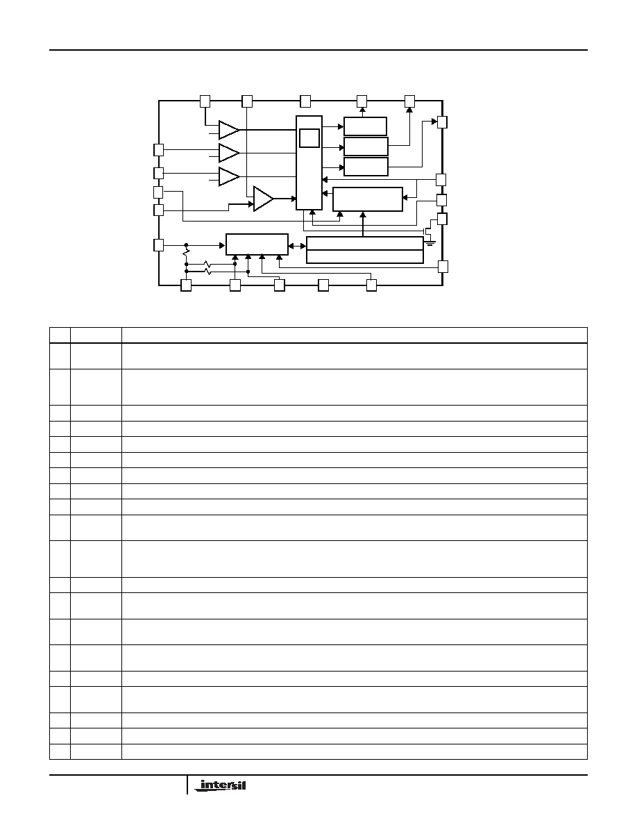
Functional Diagram
GATEH_EN
GATE_L
SCL
VDDH
VFB
DNC
GATE_M
GATE_H
18
17
16
15
14
11
13
10
9
4
5
6
7
8
+
≠
CORE-UP-FIRST
CORE-DOWN-LAST
UVLO
H
UVLO
M
UVLO
L
OSC
SE
Q
U
EN
C
E
DE
L
A
Y
LOG
I
C
CHARGE
PUMP_M
CHARGE
PUMP_H
CHARGE
PUMP_L
GND
A1
A2
NC
SDA
STATUS REGISTER
REMOTE SHUTDOWN REGISTER
2-WIRE
READY
VDDM
VDDL
SETV
REF
A0
19
20
1
2
3
ENS
12
INTERFACE
Pin Descriptions
PIN
NAME
DESCRIPTION
1
SETV
Set Voltage. This pin is used for voltage based power sequencing of supplies VDDM and VDDL.
If unused connect to ground.
2
REF
Reference voltage. This pin is used for voltage based sequencing. The voltage on this pin is compared to the voltage on the
VFB pin and provides the threshold for turn on of the GATE_M output. Either a voltage source or external resistor divider can
be used to provide the reference. If time based sequencing is used this pin should be tied to VDDH.
3
A0
Slave address pin assignment. It has an Internal pull down resistor. (>10M
typical)
4
GND
Voltage Ground.
5
A1
Slave address pin assignment. It has an Internal pull down resistor. (>10M
typical)
6
A2
Slave Address pin assignment. It has an Internal pull down resistor. (>10M
typical)
7
NC
No internal connections.
8
SDA
Serial bus data input/output pin.
9
SCL
Serial bus clock input pin.
10
READY
READY Output Pin: This open-drain output pin goes LOW while VDDH is below UVLO
H
and remains LOW for t
PURST
after
VDDH goes above UVLO
H
. READY goes HIGH after t
PURST
.
11
GATEH_EN GATE_H Enable. When this pin is HIGH and VDDH > UVLO
H
the charge pump of the GATE_H pin turns on and the output
drives HIGH. When this pin is LOW, the charge pump is disabled and the GATE_H output is LOW. An external RC time delay
can be connected between the enable signal and this pin to delay the GATE_H turn on.
12
ENS
Enable Sequence. This pin is used for time-based power sequencing of supplies VDDM and VDDL. If unused, connect to ground.
13
GATE_L
GATE_L Output: This output is connected to the gate of an (external) Power Switch "L". The GATE_L pin is driven HIGH when
charge pump L is enabled and pulled LOW when the charge pump is disabled.
14
GATE_H
GATE_H Output: This output is connected to the gate of a (external) Power Switch "H". The GATE_H pin driven HIGH when
charge pump H is enabled and pulled LOW when the charge pump is disabled.
15
GATE_M
GATE_M Output: This output is connected to the gate of a (external) Power Switch "M". The GATE_M pin driven HIGH when
charge pump M is enabled and pulled LOW when the charge pump is disabled.
16
DNC
Do not connect (must be left floating).
17
VFB
Voltage Feedback Pin. This input pin is used with voltage based power sequencing to monitor the level of a previously turned-
on supply. If unused, connect to ground.
18
VDDH
Primary supply voltage (typically 5V).
19
VDDM
Monitored Supply Voltage "M" input.
20
VDDL
Monitored Supply Voltage "L" input.
X80200, X80201, X80202, X80203, X80204
3
FN8154.0
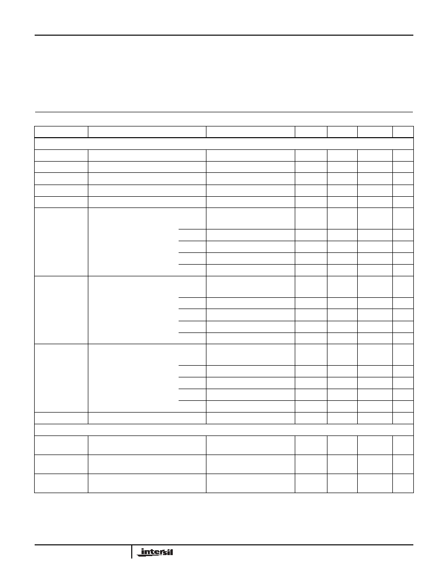
Absolute Maximum Ratings
Recommended Operating Conditions
Temperature under bias . . . . . . . . . . . . . . . . . . . . . .-65∞C to +135∞C
Storage temperature . . . . . . . . . . . . . . . . . . . . . . . .-65∞C to +150∞C
Voltage on given pin (Power Sequencing Functions):
All V
DD
pins . . . . . . . . . . . . . . . . . . . . . . . . . . . . . . . . . . . . . . . . . .7V
Temperature Range . . . . . . . . . . . . . . . . . . . . . . . . . . . -40∞C to 85∞C
Maximum Lead Temperature (Soldering 10s) . . . . . . . . . . . . . 300∞C
CAUTION: Stresses above those listed in "Absolute Maximum Ratings" may cause permanent damage to the device. This is a stress only rating and operation of the
device at these or any other conditions above those indicated in the operational sections of this specification is not implied.
Power Sequencing Control Circuits
Over the recommended operating conditions unless otherwise specified
SYMBOL
PARAMETER
TEST CONDITIONS
MIN
TYP
MAX
UNIT
DC CHARACTERISTICS ≠ Undervoltage Lockout Comparators
V
DDH
Supply Operating Range
3.05
5.5
V
V
DDM
Supply Operating Range
0.95
5.5
V
V
DDL
Supply Operating Range
0.95
5.5
V
I
DDH
Supply Current
V
DDH
= 5.5V
2.5
mA
I
DDH
Supply Current
V
DDH
= 3.1V
200
µA
UVLO
H
Undervoltage lockout for VDDH
X80200
4.425
4.5
4.575
V
X80201
4.425
4.5
4.575
V
X80202
2.95
3.0
3.05
V
X80203
2.95
3.0
3.05
V
X80204
2.95
3.0
3.05
V
UVLO
M
Undervoltage lockout for VDDM
X80200
2.2
3.0
3.05
V
X80201
2.2
2.25
2.3
V
X80202
2.2
2.25
2.3
V
X80203
2.2
2.25
2.3
V
X80204
0.875
0.9
0.925
V
UVLO
L
Undervoltage lockout for VDDL
X80200
0.875
0.9
0.925
V
X80201
0.875
0.9
0.925
V
X80202
1.65
1.7
1.75
V
X80203
0.875
0.9
0.925
V
X80204
0.875
0.9
0.925
V
V
HYS
UVLO
H,M,L
comparator Hysteresis
30
mV
DC CHARACTERISTICS ≠ Gates and Others
V
IH
Voltage Input Valid High for
ENS, SETV, GATEH_EN
VDDH x
0.7
VDDH + 0.5
V
V
IL
Voltage Input Valid Low for
ENS, SETV, GATEH_EN
-0.5
VDDH x 0.3
V
V
OL
Output LOW Voltage
(SDA, READY)
0.4
V
X80200, X80201, X80202, X80203, X80204
4
FN8154.0
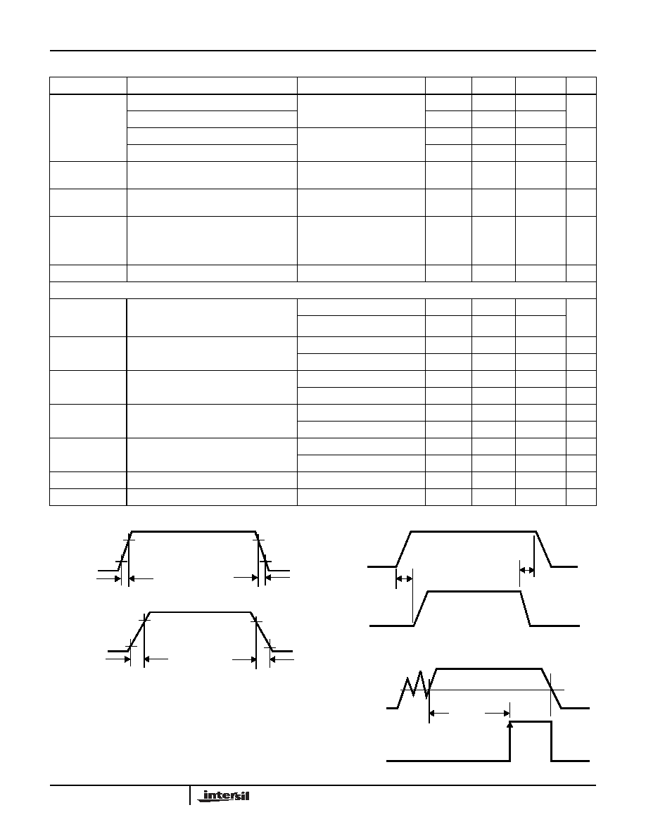
V
GATE_ON
GATE_H, GATE_M
V
DDH
= 5.5V
9.0
10
11.0
V
GATE_L
7.0
8
9.0
GATE_H, GATE_M
V
DDH
= 3.1V
7.0
8
9.0
V
GATE_L
6.0
7.0
8.0
V
GATE_OFF
Gate Voltage Drive (OFF) for GATE_H,
GATE_M, GATE_L
0
0.1
V
I
GATE_ON
Gate Current Drive (ON) for GATE_H,
GATE_M, GATE_L
(Note 1)
20
35
45
µA
I
GATE_OFF
Gate Sinking Current Drive (OFF) for
GATE_H, GATE_M, GATE_L
V
DDH
= 5.5V, V
DDM
= 0V,
V
DDL
= 0V, GATEH_EN = 0,
GATE_H = 5.5, GATE_L = 5.5,
GATE_M = 5.5 (Note 1)
9
10
11
mA
V
HYST
VFB comparator
(Note 1) 25∞C
15
20
25
mV
AC CHARACTERISTICS
t
PURST
Delayed READY Output
(READY output delayed after VDDH rises
above UVLO
H
)
V
DDH
= 5.5V
10
12
15
ms
V
DDH
= 3.1V
40
80
t
DELAY_UP
V
DDH
= 5.5V, C
GATE
= 0
600
750
900
µs
V
DDH
= 3.1V, C
GATE
= 0
6
ms
t
DELAY_DOWN
V
DDH
= 5.5V
700
800
900
µs
V
DDH
= 3.1V
6
ms
t
OFF
GATE_H, GATE_M, GATE_L
turn-off time
V
DDH
= 5.5V, (Note 1)
40
µs
V
DDH
= 3.1V, (Note 1)
80
µs
t
ON
GATE_H, GATE_M, GATE_L
turn-on time
V
DDH
= 5.5V, (Note 1)
0.5
0.6
0.7
ms
V
DDH
= 3.1V, (Note 1)
2
5
ms
t
R
V
DDH
Rise Time
(Note 1)
1.0
µs
t
F
V
DDH
Fall Time
(Note 1)
1.0
µs
Power Sequencing Control Circuits
Over the recommended operating conditions unless otherwise specified (Continued)
SYMBOL
PARAMETER
TEST CONDITIONS
MIN
TYP
MAX
UNIT
VDDH
t
R
t
F
GATE_H, M, L
t
ON
t
OFF
GATE_L
GATE_M
t
DELAY_UP
t
DELAY_DOWN
t
PURST
UVLO
H
VDDH
READY
X80200, X80201, X80202, X80203, X80204
5
FN8154.0
Equivalent AC Output Load Circuit for
VDDH = 5V
Symbol Chart
Serial bus Interface Electrical Characteristics
SYMBOL
PARAMETER
TEST CONDITIONS
MIN
MAX
UNIT
V
IL
Signal Input Low Voltage
0.8
V
V
IH
Signal Input High Voltage
2.0
V
V
OL
Signal Output Low Voltage
(Note 1), I
pullup
4mA
0.4
V
C
BUS
Capacitive Load per bus segment
(Note 1)
400
pF
Capacitance
SYMBOL
PARAMETER
TEST CONDITIONS
MAX
UNIT
C
OUT
Output Capacitance (SDA)
V
OUT
= 0V, (Note 1)
8
pF
C
IN
Input Capacitance (SCL)
V
IN
= 0V, (Note 1)
6
pF
NOTE:
1.
Guaranteed by device characterization.
VDDH
SDA, READY
30pF
2.06k
AC Test Conditions
Input pulse levels
V
CC
x 0.1 to V
CC
x 0.9
Input rise and fall times
10ns
Input and output timing levels
V
CC
x 0.5
Output load
Standard output load
Must be
steady
Will be
steady
May change
from LOW
Will change
from LOW
to HIGH
May change
from HIGH
to LOW
Will change
from HIGH
to LOW
Don't Care:
Changes
Allowed
Changing:
State Not
Known
N/A
Center Line
is High
Impedance
WAVEFORM
INPUTS
OUTPUTS
to HIGH
X80200, X80201, X80202, X80203, X80204
6
FN8154.0
Timing Diagrams
Bus Interface AC Timing
SYMBOL
PARAMETER
TEST
CONDITION
SMBUS
2-WIRE BUS
UNITS
MIN
MAX
MIN
MAX
f
SCL
Clock Frequency
10
100
400
kHz
t
CYC
Clock Cycle Time
10
2.5
µs
t
HIGH
Clock High Time
4.0
50
0.6
µs
t
LOW
Clock Low Time
4.7
1.3
µs
t
SU:STA
Start Set-up Time
4.7
0.6
µs
t
HD:STA
Start Hold Time
4.0
0.6
µs
t
SU:STO
Stop Set-up Time
4.0
0.6
µs
t
SU:DAT
SDA Data Input Set-up Time
250
100
ns
t
HD:DAT
SDA Data Hold Time
300
0
ns
t
R
SCL and SDA Rise Time: TR = (V
ILMAX
- 0.15) to
(V
IHMIN
+0.15)
(Note 1)
1000
300
ns
t
F
SCL and SDA Fall Time: TF = (V
IHMIN
- 0.15) to
(V
ILMAX
- 0.15)
(Note 1)
300
300
ns
t
AA
SCL Low to SDA Data Output Valid Time
(Note 1)
550
1100
250
1100
ns
t
DH
SDA Data Output Hold Time
(Note 1)
300
0
ns
T
I
Noise Suppression Time Constant at SCL and SDA inputs
(Note 1)
50
50
ns
t
BUF
Bus Free Time (Prior to Any Transmission)
(Note 1)
4.7
1.3
µs
t
SU:A
A0, A1, A2 Set-up Time
0
0
ns
t
HD:A
A0, A1, A2 Hold Time
0
0
ns
FIGURE 1. BUS TIMING
t
SU:STO
t
HIGH
t
SU:STA
t
HD:STA
t
HD:DAT
t
SU:DAT
SCL
SDA IN
SDA OUT
t
F
t
LOW
t
HD:DAT
t
R
t
DH
t
AA
t
BUF
t
HD:STO
t
BUF
t
HD:A
SCL
SDA IN
A2, A1, A0
t
SU:A
CLK 1
CLK 9
SLAVE ADDRESS BYTE
START
FIGURE 2. ADDRESS PIN TIMING
X80200, X80201, X80202, X80203, X80204

7
FN8154.0
Principles of Operation
Power Sequencing Control (PSC)
The Intersil X80200 supports a variety of sequencing
applications. The sequencing can be voltage-based or time-
based. Some examples are shown in Figure , Figure , and
Figure in the Applications section. The X80200 allows for
designs that can control the power sequencing of up to three
voltage supplies. For systems with more than three supplies,
the X80200 may be cascaded.
Basic Functions
VDDH is the primary voltage for the X80200. Once VDDH
rises above the primary undervoltage lockout level (UVLO
H
)
for time t
PURST
, the READY output goes HIGH indicating
that the supply power is good. By connecting READY
directly to GATEH_EN, the GATE_H output goes high
immediately, turning on the power FET connected in series
with VDDH. The system primary voltage may be delayed by
using an external RC circuit between READY and
GATEH_EN.
VDDH must be stable before VDDM and VDDL supplies are
monitored and power sequencing begins.
The second supply voltage (I/O supply) is monitored by the
VDDM pin. VDDM must be greater than the I/O supply
undervoltage lockout level (UVLO
M
) prior to any activation of
the GATE_M output. The VDDM voltage is used to turn on
the charge pump that drives the GATE_M output.
The third supply (core supply) is monitored by the VDDL pin.
VDDL must be greater than the core supply undervoltage
lockout level (UVLO
L
) prior to any activation of the GATE_L
output. The VDDL voltage is used to turn on the charge
pump that drives the GATE_M output.
Power Sequencing Functions
X80200 provides two options for power sequencing. In time
based sequencing, the ENS (Enable Sequence) input
signals that the core and I/O voltages are to turn on with a
fixed time relationship. In voltage based sequencing, the
SETV (Set Voltage) initiates turn-on of the core voltage. The
I/O voltage remains off until the core voltage reaches a set
threshold.
In both cases the X80200 uses a core-voltage first and core
voltage-last power up/down algorithm.
TIME-BASED POWER SEQUENCING
A rising edge (LOW to HIGH) transition of the ENS pin turns
on the charge pump that drives the GATE_L output.
A falling edge (HIGH to LOW) transition of the ENS signal
turns off the charge pump that drives the GATE_M output.
This technique provides a "forced" core-voltage-first power
up and core-voltage-last power down algorithm. The ENS
signal does not control the ramp up/down rates of the
GATE_M or GATE_L outputs.
In the absence of an externally provided ENS signal, the
ENS pin can be connected in a number of different ways.
∑ ENS can connect to the VDDH pin. In this case, the
GATE_H and GATE_L outputs are enabled at the same
time. GATE_H could be delayed by using an external RC
timer between READY and GATEH_EN to provide a
sequence where VDDL is the first supply voltage applied
to the system.
∑ ENS can connect to a delayed READY signal, so that the
VDDL voltage follows the VDDH voltage by a fixed time.
∑ ENS can connect to the system side of the VDDH FET, so
the VDDL voltage will follow immediately after the primary
supply is applied to the system.
See "Functional Description" on page 7 for details on timing
and ramp-up.
VOLTAGE-BASED POWER SEQUENCING
In this configuration, the drain of the "L" MOSFET is
connected to the VFB input of the X80200, the ENS pin is
tied to ground and a resistor divider provides a reference
voltage to the REF pin.
A LOW to HIGH transition of the SETV pin turns on the
GATE_L output. This turns on the "L" MOSFET. Once the
drain of this FET reaches the REF level, GATE_M turns on.
Since the trigger for the GATE_M output is selected by a
threshold level, the user has the ability to specify relative
core and I/O voltage sequencing.
System Monitoring and Remote Shutdown
The X80200 Status Register contains fault detection bits that
indicate the status of the GATE_H, GATE_M, and GATE_L
pins. These bits are Stat_GATEH, Stat_GATEM, and
Stat_GATEL. The status register can be read via 2-wire bus.
This feature allows for system monitoring of the power
sequencing of supplies.
The system can turn off the FETs by writing to the Remote
Shutdown Register through the 2-wire interface. There are
three turn-off selections. See "Remote Shutdown Register
(RSR) (Volatile)" on page 10 for more details.
Functional Description
Voltage Inputs. The X80200 has three voltage monitors for
power sequencing: the VDDH (primary voltage), VDDM (I/O
voltage), and VDDL (core voltage). These voltage monitors
operate independently of each other.
PRIMARY VOLTAGE VDDH
This voltage is the primary voltage for the device and is
required before X80200 can power sequence VDDM and
VDDL. As VDDH powers up, it is compared to an internal
UVLO
H
reference. This undervoltage lockout level is preset
at the factory. For information on this setting, see Ordering
Information. For custom programmed levels, contact Intersil.
X80200, X80201, X80202, X80203, X80204

8
FN8154.0
The READY output pin reflects the condition of the VDDH
input. READY is LOW as long as VDDH is below UVLO
H
and remains LOW for a period of t
PURST
after VDDH
crosses UVLO
H
, see Figure 4. Once VDDH rises above
UVLO
H
and remains stable for t
PURST
, the READY output
turns ON. If READY connects directly to the GATEH_EN pin,
then the GATE_H charge pump turns on immediately. The
turn on of the Gate_H charge pump can be delayed by using
an external filter (RC filter) connected between the READY
and GATEH_EN pins.
When VDDH drops below the UVLO
H
threshold, READY
goes inactive immediately. For more details on this turn-off
mechanism, See "Power Supply Failure Conditions" on
page 9.
SECONDARY VOLTAGES VDDM AND VDDL
The VDDM and VDDL voltage inputs each have their own
undervoltage lockout settings, UVLO
M
, and UVLO
L
,
respectively. Each undervoltage lockout level is preset at the
factory. For information on these settings, See Ordering
Information. For custom programmed levels, contact Intersil.
The GATE_M and GATE_ L charge pumps are OFF as long
as VDDM, and VDDL are below their respective UVLO trip
points. When READY is active and VDDM and VDDL go
above their UVLO thresholds, the GATE_M and GATE_L
charge pumps can be turned ON when activated as part of
the power sequence desired. If VDDL or VDDM drop below
the UVLO level the charge pumps turn off. For more details
on this turn-off mechanism, See "Power Supply Failure
Conditions" on page 9.
Sequence Delay Logic. This block contains the logic
circuits that implement the power-up and power-down
sequencing of the VDDH (GATE_H), VDDM (GATE_M), and
VDDL (GATE_L) voltages. The sequencing protocol has a
built-in "core-first-up and core-down-last" algorithm. On
power-up the GATE_L signal turns on first, followed by
GATE_M signal. During the power-down, the GATE_M turns
off first and the GATE_L signal follows.
The sequencing of the power supplies is primarily controlled
and regulated via the SETV and the ENS (enable sequence)
pins.
All charge pumps are designed to ramp up their respective
gates at the same slew rate for the same load.
Time Based Power Sequencing (ENS option)
The ENS (Enable Sequence) pin controls the start of the
ramp up/ramp down sequence for GATE_M and GATE_L in
the time domain. (See Figure 3.)
ENS is an edge-triggered input. A rising edge (LOW to
HIGH) on the ENS input turns on the charge pump that
drives the GATE_L output. The slew rate of the GATE_L
output depends on the external MOSFET and any load
connected to it. (See Electrical Table). After a t
DELAY_UP
time, the GATE_M charge pump turns ON. Again the slew
rate is dependent on the load connected to GATE_M output.
The falling edge transition on the ENS pin (HIGH to LOW)
turns off the charge pump that drives the GATE_M output.
After a t
DELAY_DOWN
time period, the GATE_L charge
pump turns OFF.
Voltage Based Power Sequencing (SETV Option)
Using the SETV pin allows for a voltage based sequencing
of the GATE_L and GATE_M outputs. SETV is an edge
triggered input signal. A LOW to HIGH transition on SETV
immediately turns ON the charge pump for GATE_L. The
GATE_L output then starts ramping up. In this configuration,
the drain of the MOSFET "L" connects to the VFB pin and
this voltage is compared to an external reference applied to
the REF pin. The comparator turns on the charge pump for
GATE_M once the voltage on VFB exceeds the voltage on
REF. (See Figure 5.)
The voltage sequencing comparator has a 30mV hysteresis,
so the GATE_M output does not oscillate as the core voltage
powers up.
A High to Low transition of SETV turns OFF charge pump M
and GATE_M is pulled low. After a t
DELAY_DOWN
time
period, charge pump L turns off and GATE_L is pulled low.
t
DELAY_UP
ENS
GATE_L
GATE_M
t
DELAY_DOWN
FIGURE 3. TIME BASED SEQUENCING OF GATE_M AND
GATE_L
t
PURST
UVLO
H
VDDH
READY
FIGURE 4. VDDH/READY SEQUENCING
X80200, X80201, X80202, X80203, X80204

9
FN8154.0
Power Supply Failure Conditions
Should there be a power failure of VDDH, GATE_H,
GATE_M and GATE_L charge pumps are all turned OFF
when VDDH falls below the UVLO
H
threshold.
Should there be a failure of the VDDM supply, the GATE_M
charge pump turns off when VDDM falls below the UVLO
M
threshold. After a t
DELAY_DOWN
time period, the GATE_L
charge pump turns OFF.
Should there be a failure of the VDDL supply, the GATE_L
and GATE_M charge pumps both turn off when VDDL falls
below the UVLO
L
threshold.
Remote Monitoring Functions
The X80200 can monitor the status of the GATE_H,
GATE_M, and GATE_L charge pump control signals. This
allows an indirect way to monitor system voltages. The
volatile status bits: Stat_GATEH, Stat_GATEM, and
Stat_GATEL indicate the status of GATE_H, GATE_M and
GATE_L output control signals, respectively. If the bit is a "1",
then the charge pump is being turned on. If the bit is a "0",
the output is turned off. Since the bits reflect the internal
control signal and not the state of the output, external
loading that prevents the charge pump from reaching the
desired FET gate drive voltage will not be detected by
reading the register.
These status bits can be read via the 2-wire serial bus. Refer
to Status Register section for more information on how to
read this register.
Several X80200 devices can be used to monitor many
system voltages on different system cards on a backplane.
Each X80200 has 3 slave address pins allowing up to 8
X80200 to be used on the same bus.
X80200 provides the user the ability to remotely turn-off the
gates through software. (See "Remote Shutdown Register
(RSR) (Volatile)" on page 10 for more information.)
SETV
FET "L"
GATE_M
t
DELAY_DOWN
GATE_L
(VFB)
DRAIN
REF
REF
FIGURE 5. VOLTAGE BASED SEQUENCING OF GATE_M
AND GATE_L
VDDH
VDDM
VDDL
GATE_H
GATE_M
GATE_L
t
DELAY_DOWN
VDDH
VDDM
VDDL
FAILS
FAILS
FAILS
FIGURE 6. GATE CONTROL DURING INDIVIDUAL POWER
FAIL CONDITIONS
X80200, X80201, X80202, X80203, X80204

10
FN8154.0
Register Information
The Register Block is organized as follows:
∑ Status Register (SR) (1 Byte). Located at address 00h.
∑ Remote Shut Down Register (RSR) (1 Byte). Located at
address FFh.
The Status Register provides the user a mechanism for
checking the status of GATE_H, GATE_M and GATE_L.
These bits are volatile and are read only.
The gate status values in the Status Register can be read at
any time by performing a random read operation. Only one
byte is returned by each read operation. The master should
supply a stop condition following the output byte to be
consistent with the bus protocol.
STAT_GATEH: GATEH Status Flag (volatile)
STAT_GATEH will be set to `1' when the GATE_H charge
pump is turned on. It will be reset to `0' when the GATE_H
charge pump is turned off.
STAT_GATEM: GATEM Status Flag (volatile)
STAT_GATEM will be set to `1' when GATE_M charge pump
is turned on. It will be reset to `0' when the GATE_M charge
pump is turned off.
STAT_GATEL: GATEL Status Flag (volatile)
STAT_GATEL will be set to `1' when GATE_L charge pump
is turned on. It will be reset to `0' when the GATE_L charge
pump is turned off.
The status register also contains a WEL bit that controls
write operations to the Shutdown Register. Bits 7, 6, 5, and 4
should always be set to `0'.
WEL: Write Enable Latch (Volatile)
The WEL bit controls the access to the Remote Shutdown
Register (RSR). This bit is a volatile latch that powers up in
the LOW (disabled) state. While the WEL bit is LOW, writes
to the RSR will be ignored (no acknowledge will be issued
after the Data Byte). The WEL bit is set by writing a "1" to the
WEL bit and zeroes to the other bits of the status register.
The X80200 provides the user with a software shutdown of
GATE_H, GATE_L and GATE_M. This over-rides the normal
output control.
A write operation with data 01h to the RSR will immediately
turn off GATE_M followed by GATE_L. The GATE_L turn off
is delayed by t
DELAY_DOWN
.
A write operation with data 02 to the RSR will turn off
GATE_H.
A write operation with data 03 to RSR will shutdown all
gates. GATE_H turn off at the same time as GATE_M.
GATE_L turns off after a delay of t
DELAY_DOWN
.
A write operation with data 00h to the RSR will remove the
software override function. Assuming all supplies are good,
the X80200 will return to the previous state by first turning on
GATE_H and GATE_L. Then, GATE_M is turned on
according to the power sequencing mode chosen.
Bits 7, 6, 5, 4, 3 and 2 of the Remote Shutdown Register
should always be set to `0'.
The data in the RSR can be read by performing a random
read operation to the RSR. The data in the RSR powers up
in `0' state.
Bus Interface Information
Interface Conventions
The device supports a bidirectional bus oriented protocol.
The protocol defines any device that sends data onto the
bus as a transmitter, and the receiving device as the
receiver. The device controlling the transfer is called the
master and the device being controlled is called the slave.
The master always initiates data transfers, and provides the
clock for both transmit and receive operations. Therefore,
the devices in this family operate as slaves in all
applications.
Status Register (Volatile)
7
6
5
4
3
2
1
0
0
0
0
0
STAT_
GATEH
STAT_
GATEM
STAT_
GATEL
WEL
Remote Shutdown Register (RSR) (Volatile)
RSR
DATA
GATE
SHUTDOWN
SEQUENCE
01
GATE_M,
GATE_L
GATE_M turns off, then after time
t
DELAY_DOWN
GATE_L turns off.
02
GATE_H
Immediate turn off of GATE_H
03
GATE_H,
GATE_M,
GATE_L
GATE_H and GATE_M turn off, then after
time t
DELAY_DOWN
GATE_L turns off.
00
no override
X80200 returns to previous condition,
assuming all supplies are good, GATE_H
and GATE_L turn on, then GATE_M turns
on according to the chosen sequence
mode.
X80200, X80201, X80202, X80203, X80204
11
FN8154.0
SERIAL CLOCK AND DATA
Data states on the SDA line can change only during SCL
LOW. SDA state changes during SCL HIGH are reserved for
indicating start and stop conditions. (See Figure 7.)
SERIAL START CONDITION
All commands are preceded by the start condition, which is a
HIGH to LOW transition of SDA when SCL is HIGH. The
device continuously monitors the SDA and SCL lines for the
start condition and will not respond to any command until
this condition has been met. (See Figure 8.)
SERIAL STOP CONDITION
All communications must be terminated by a stop condition,
which is a LOW to HIGH transition of SDA when SCL is
HIGH, followed by a HIGH to LOW transition on SCL. After
going LOW, SCL can stay LOW or return to HIGH. (See
Figure 8.)
Slave Address Byte
Following a START condition, the master must output a
Slave Address Byte. This byte consists of three parts:
∑ The Device Type Identifier which consists of the most
significant four bits of the Slave Address. The Device Type
Identifier MUST be set to 1010 in order to select the
device.
∑ The next 3 bits (SA3 - SA1) are slave address bits. These
bits are compared to the status of the input pins A2≠A0.
∑ The Least Significant Bit of the Slave Address (SA0) Byte
is the R/W bit. This bit defines the operation to be
performed on the device being addressed (as defined in
the bits SA2 - SA1). When the R/W bit is "1", then a READ
operation is selected. A "0" selects a WRITE operation.
Word Address
The next 8 bits following the slave byte, BA7≠BA0,
determine the portion of the device accessed. If all `0's, then
Status Register (SR) is selected. If all `1's, then the Remote
Shutdown Register (RSR) is selected.
Serial Acknowledge
Acknowledge is a software convention used to indicate
successful data transfer. The transmitting device, either
master or slave, will release the bus after transmitting eight
bits. During the ninth clock cycle, the receiver will pull the
SDA line LOW to acknowledge that it received the eight bits
of data. (See Figure 9.)
The device will respond with an acknowledge after
recognition of a start condition and if the correct Device
Identifier and Select bits are contained in the Slave Address
Byte. If a write operation is selected, the device will respond
with an acknowledge after the receipt of each subsequent
eight bit word. The device will acknowledge all incoming data
and address bytes, except for the Slave Address Byte when
the Device Identifier and/or Select bits are incorrect.
Write Operation
For a write operation, the device requires the Slave Address
Byte and a Word Address Byte. This gives the master
access to the registers. After receipt of the Word Address
Byte, the device responds with an acknowledge, and awaits
the next eight bits of data. After receiving the 8 bits of the
Data Byte, the device again responds with an acknowledge.
The master then terminates the transfer by generating a stop
condition. (See Figure 11, See Figure 1 for bus timing.)
In order to perform a write operation to Remote Shutdown
Register, the Write Enable Latch (WEL) bit must first be set.
SCL
SDA
DATA STABLE
DATA
CHANGE
DATA STABLE
FIGURE 7. VALID DATA CHANGES ON THE SDA BUS
SCL
SDA
START
STOP
FIGURE 8. VALID START AND STOP CONDITIONS
8
9
1
SCL FROM
MASTER
DATA OUTPUT
FROM TRANSMITTER
DATA OUTPUT
FROM RECEIVER
START
ACKNOWLEDGE
FIGURE 9. ACKNOWLEDGE RESPONSE FROM RECEIVER
X80200, X80201, X80202, X80203, X80204
12
FN8154.0
Read Operation
A Read operation is initiated in the same manner as a write
operation with the exception that the R/W bit of the Slave
Address Byte is set to one.
Prior to issuing the Slave Address Byte with the R/W bit set to
one, the master must first perform a "dummy" write operation.
The master issues the start condition and the Slave Address
Byte, receives an acknowledge, then issues the Word Address
Byte. After acknowledging receipt of the Word Address Byte,
the master immediately issues another start condition and the
Slave Address Byte with the R/W bit set to one. This is followed
by an acknowledge from the device and then by the data byte
containing the register contents. The master terminates the
read operation by responding with a no-acknowledge and then
issuing a stop condition. The ninth clock cycle of the read
operation is not a "don't care." To terminate a read operation,
the master must either issue a stop condition during the
ninth cycle or hold SDA HIGH during the ninth clock cycle
and then issue a stop condition.
See Figure 12 for the address, acknowledge, and data
transfer sequence. See Figure 1 for bus timing.
Operational Notes
The device powers-up in the following state:
∑ The device is in the low power standby state.
∑ The WEL bit is set to `0'. It is not possible to write to the
device.
∑ The WEL bit must be set to allow write operations.
∑ SDA pin is the input mode.
∑ The data in the RSR powers up in `0' state.
SA6
SA7
SA5
SA2
SA1
SA0
DEVICE TYPE
IDENTIFIER
READ/
SA4
R/W
1
0
1
0
WRITE
ADDRESS
INTERNAL
DEVICE
A2
A1
A0
BIT SA0
OPERATION
0
WRITE
1
READ
BA7
BA6
BA5
BA4
BA3
BA2
BA1
BA0
0
0
0
0
0
0
0
1
1
1
1
1
1
1
D7
DATA BYTE
D6
D5
D4
D3
D2
D1
D0
SLAVE ADDRESS
SR
RSR
SA3
WORD ADDRESS
0
1
FIGURE 10. ADDRESS FORMAT
X80200, X80201, X80202, X80203, X80204
13
FN8154.0
Application Section
S
T
A
R
T
S
T
O
P
DATA
A
C
K
A
C
K
SDA BUS
SIGNALS FROM
THE SLAVE
SIGNALS FROM
THE MASTER
0
A
C
K
WORD
ADDRESS
1
0
1
0
SLAVE
ADDRESS
DEVICE
ID
A0
A1
A2
FIGURE 11. BYTE WRITE SEQUENCE
A
C
K
S
T
A
R
T
S
T
O
P
DATA
S
T
A
R
T
SDA BUS
SIGNALS FROM
THE SLAVE
SIGNALS FROM
THE MASTER
WORD
ADDRESS
A
C
K
SLAVE
ADDRESS
0
1
0
1
0
DEVICE
ID
A
C
K
SLAVE
ADDRESS
1
1
0
1
0
DEVICE
ID
A0
A1
A2
A0
A1
A2
A
C
K
S
T
A
R
T
S
T
O
P
DATA
S
T
A
R
T
SDA BUS
SIGNALS FROM
THE SLAVE
SIGNALS FROM
THE MASTER
WORD
ADDRESS
A
C
K
SLAVE
ADDRESS
0
1
0
1
0
DEVICE
ID
A
C
K
SLAVE
ADDRESS
1
1
0
1
0
DEVICE
ID
A0
A1
A2
A0
A1
A2
FIGURE 12. READ SEQUENCE
DC-DC
#1
DC-DC
#2
DC-DC
#3
HOT S
W
AP
CONTROLLE
R
-4
8V
BACK
PLANE
/COMMUNICA
TION
BACKP
LANE
OPTIONAL
SMBus
SMBus
H (OPTIONAL)
PRIMARY
I/O VOLTAGES
CORE VOLTAGES
SLA
V
E
ADDRE
SS
PULL UP
TO SET
ADDRESS HIGH
SYSTEM
COMPONENTS &
BOARD SUPPLIES
I/O SUPPLY
CORE SUPPLY
µP/
ASICs/
FPGA
VCORE
V I/O
Primary
3.3V
5V
5V
2.7V
2.5V
2.0V
1.8V
1.25V
0.9V
3.3V
2.5V
1.35V
1.25V
L
M
RC DELAY
X80200
VDDH
VDDM
SETV
VDDL
GATEH_EN
SDA
SCL
GND
A2
A0
ENS
GATE_L
GATE_M
GATE_H
VFB
REF
READY
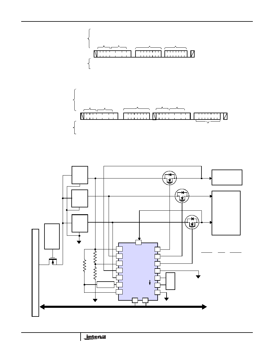
FIGURE 13. TELECOM BACKPLACE/SYSTEM POWER SUPPLY VOLTAGE BASED POWER SEQUENCING
X80200, X80201, X80202, X80203, X80204
14
FN8154.0
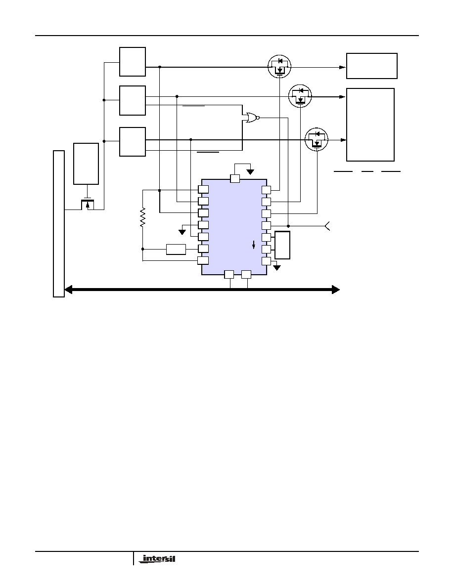
DC-DC
#1
DC-DC
#2
DC-DC
#3
HOT SW
A
P
CONTROLLER
-48V
BACKPLANE/COMMUNICA
TION BACKPLANE
OPTIONAL
SMBus
SMBus
H (OPTIONAL)
PRIMARY
I/O VOLTAGES
CORE VOLTAGES
SL
A
V
E
ADDRE
S
S
PULL UP
TO SET
ADDRESS HIGH
OPTION
FORCED
SEQUENCING
SYSTEM
COMPONENTS &
BOARD SUPPLIES
I/O SUPPLY
CORE SUPPLY
µP/
ASICs/
FPGA
VCORE
V I/O
Primary
3.3V
5V
5V
2.7V
2.5V
2.0V
1.8V
1.25V
0.9V
3.3V
2.5V
1.35V
1.25V
VCORE
L
M
PGOOD1
PGOOD2
DELAY
VDDH
VDDM
SETV
VDDL
GATEH_EN
SDA
SCL
GND
A2
A0
ENS
GATE_L
GATE_M
GATE_H
VFB
REF
READY
FIGURE 14. TELECOM BACKPLACE/SYSTEM POWER SUPPLY TIME BASED POWER SEQUENCING
X80200, X80201, X80202, X80203, X80204

15
FN8154.0
DC-DC
#1
OPTION
SMBus
SMBus
H (OPTIONAL)
PRIMARY
V I/O
V
ID4:ID0
SLA
V
E
ADD
R
ES
S
PULL UP
TO SET
ADDRESS HIGH
OPTIONAL
FORCED
SEQUENCING
SYSTEM
COMPONENTS &
BOARD SUPPLIES
VCORE V I/O Primary
3.3V
5V
5V
2.7V
2.5V
2.0V
1.8V
1.25V
0.9V
3.3V
2.5V
1.35V
1.25V
DC-DC
#2
V
ID4:IDO
VCORE
PWRGD
SCL
SDA
VRM
POWER
SUPPLY
I/O SUPPLY
CORE SUPPLY
µP/
ASICs/
FPGA
M
POWER SEQUENCING (TIME BASED MODE)
USING POWER GOOD SIGNALS
DELAY
10
7,8,55-57
5
9
OUTEN
PGOOD1
53
NC
X80200
VDDH
VDDM
SETV
VDDL
GATEH_EN
SDA
SCL
GND
A2
A0
ENS
GATE_L
GATE_M
GATE_H
VFB
REF
READY
FIGURE 15. POWER SEQUENCING OF VRM SUPPLIES
X80200, X80201, X80202, X80203, X80204
16
All Intersil U.S. products are manufactured, assembled and tested utilizing ISO9000 quality systems.
Intersil Corporation's quality certifications can be viewed at www.intersil.com/design/quality
Intersil products are sold by description only. Intersil Corporation reserves the right to make changes in circuit design, software and/or specifications at any time without
notice. Accordingly, the reader is cautioned to verify that data sheets are current before placing orders. Information furnished by Intersil is believed to be accurate and
reliable. However, no responsibility is assumed by Intersil or its subsidiaries for its use; nor for any infringements of patents or other rights of third parties which may result
from its use. No license is granted by implication or otherwise under any patent or patent rights of Intersil or its subsidiaries.
For information regarding Intersil Corporation and its products, see www.intersil.com
FN8154.0
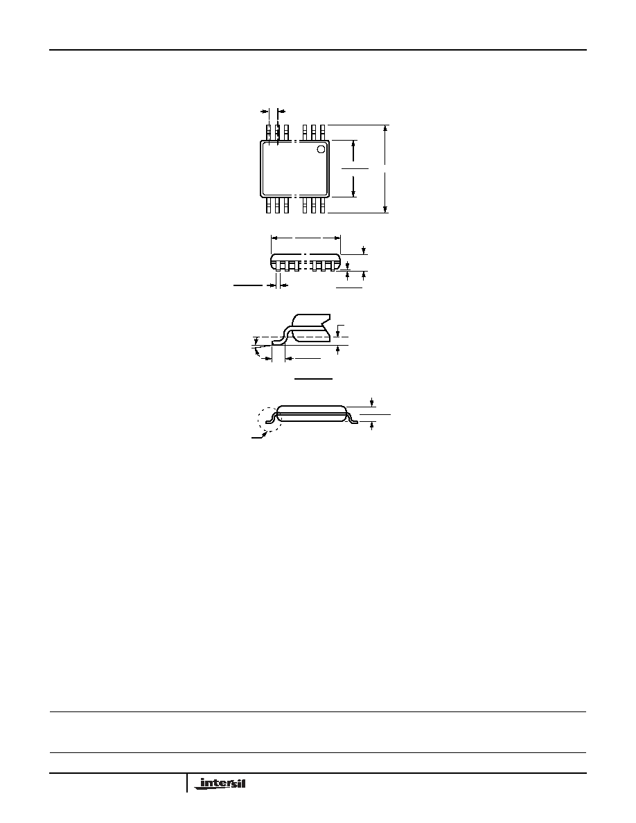
Packaging Information
NOTE: ALL DIMENSIONS IN INCHES (IN PARENTHESES IN MILLIMETERS)
20-Lead Plastic, TSSOP, Package Code V20
See Detail "A"
.031 (.80)
.041 (1.05)
.169 (4.3)
.177 (4.5)
.252 (6.4) BSC
.025 (.65) BSC
.252 (6.4)
.260 (6.6)
.002 (.05)
.006 (.15)
.041 (1.05)
.0075 (.19)
.0118 (.30)
0∞ - 8∞
.010 (.25)
.019 (.50)
.029 (.75)
Gage Plane
Seating Plane
Detail A (20X)
X80200, X80201, X80202, X80203, X80204