1
Æ
FN8167.1
CAUTION: These devices are sensitive to electrostatic discharge; follow proper IC Handling Procedures.
1-888-INTERSIL or 1-888-468-3774
|
Intersil (and design) is a registered trademark of Intersil Americas Inc.
XDCP is a trademark of Intersil Americas Inc. Copyright Intersil Americas Inc. 2005. All Rights Reserved
All other trademarks mentioned are the property of their respective owners.
X9252
Low Power + Quad 256-tap + 2-Wire Bus + Up/Down Interface
Quad Digitally-Controlled (XDCPTM)
Potentiometer
The X9252 integrates 4 digitally controlled potentiometers
(XDCP) on a monolithic CMOS integrated circuit.
The digitally controlled potentiometers are implemented
using 255 resistive elements in a series array. Between each
pair of elements are tap points connected to wiper terminals
through switches. The position of each wiper on the array is
controlled by the user through the Up/Down (U/D) or 2-wire
bus interface. The wiper of each potentiometer has an
associated volatile Wiper Counter Register (WCR) and four
non-volatile Data Registers (DRs) that can be directly written
to and read by the user. The contents of the WCR controls
the position of the wiper on the resistor array through the
switches. At power-up, the device recalls the contents of the
default data registers DR00, DR10, DR20, DR30, to the
corresponding WCR.
Each DCP can be used as a three-terminal potentiometer or
as a two terminal variable resistor in a wide variety of
applications including the programming of bias voltages, the
implementation of ladder networks, and three resistor
programmable networks.
Features
∑ Quad Solid State Potentiometer
∑ 256 Wiper Tap Points-0.4% Resolution
∑ 2-Wire Serial Interface for Write, Read, and Transfer
Operations of the Potentiometer
∑ Up/Down Interface for Individual Potentiometers
∑ Wiper Resistance: 40
Typical
∑ Non-Volatile Storage of Wiper Positions
∑ Power On Recall. Loads Saved Wiper Position on Power-
Up.
∑ Standby Current < 20µA Max
∑ Maximum Wiper Current: 3mA
∑ V
CC
: 2.7V to 5.5V Operation
∑ 2.8k
,10k, 50k, 100k Version of Total Pot Resistance
∑ Endurance: 100, 000 Data Changes per Bit per Register
∑ 100 yr. Data Retention
∑ 24 Ld TSSOP
∑ Pb-Free Plus Anneal Available (RoHS Compliant)
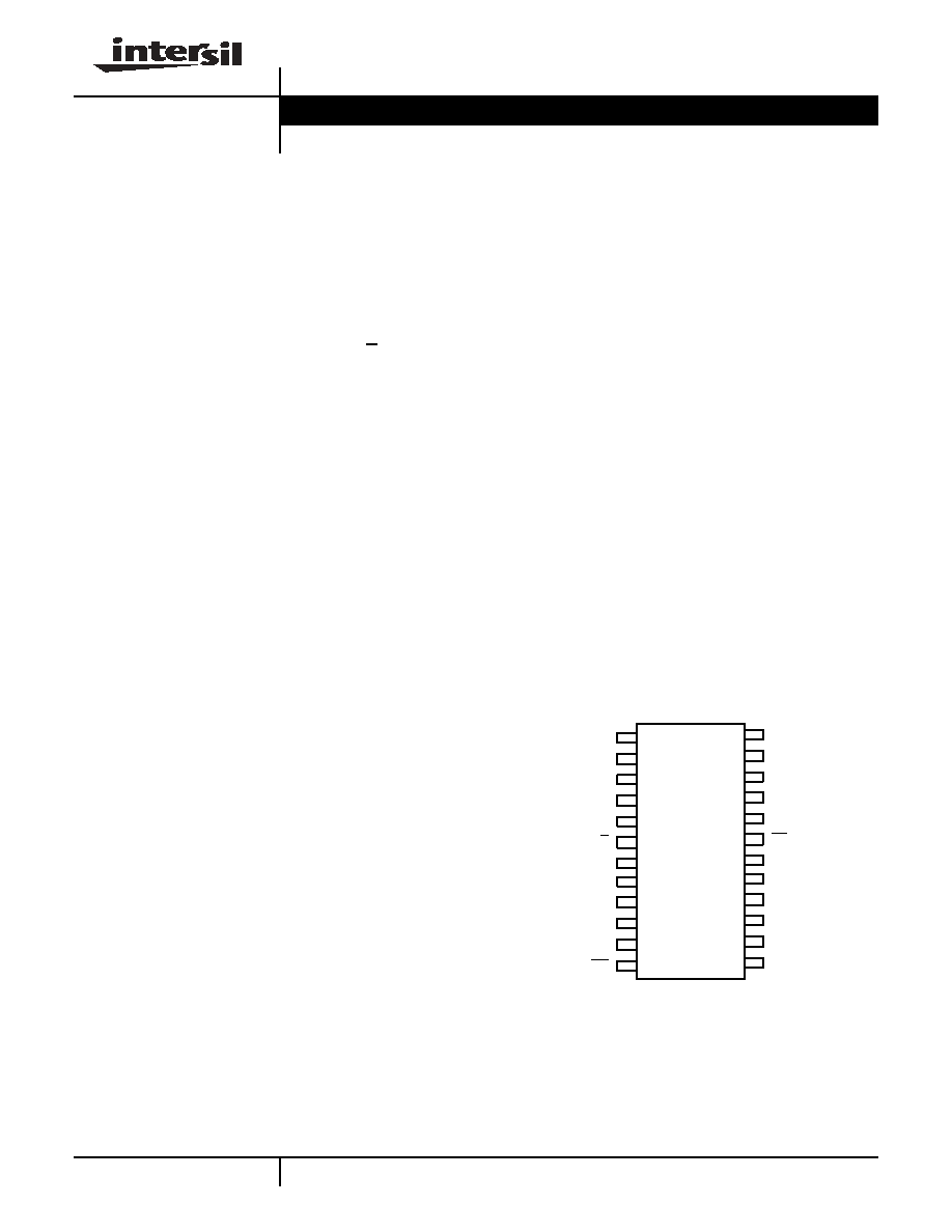
Pinout
X9252
(24 LD TSSOP)
TOP VIEW
R
H2
R
H3
R
W2
1
2
3
4
5
6
7
14
20
19
18
17
16
15
X9252
DS0
DS1
A0
R
W3
U/D
R
L3
SCL
R
L2
V
SS
R
L1
R
W0
CS
R
H0
R
L0
R
W1
R
H1
V
CC
8
9
10
13
WP
A2
11
12
SDA
A1
24
23
22
21
Data Sheet
September 14, 2005
2
FN8167.1
September 14, 2005
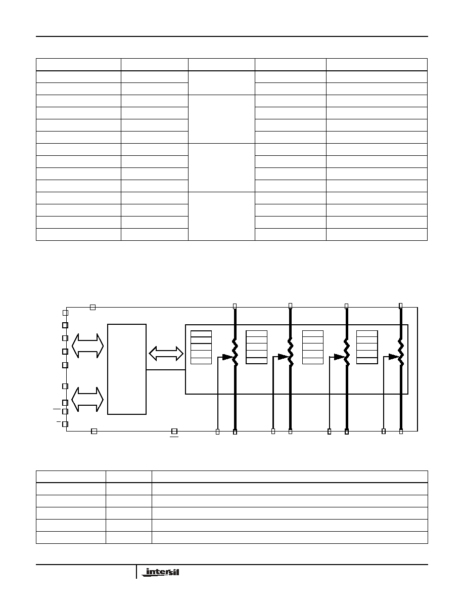
Functional Diagram
Ordering Information
PART NUMBER
PART MARKING
R
TOTAL
(k
)
TEMP RANGE (∞C)
PACKAGE
X9252YV24I-2.7
X9252YV G
2.8
-40 to 85
24 Ld TSSOP (4.4mm)
X9252YV24IZ-2.7 (Note)
X9252YV Z G
-40 to 85
24 Ld TSSOP (4.4mm) (Pb-free)
X9252WS24I-2.7
X9252WS G
10
-40 to 85
24 Ld SOIC (300 mil)
X9252WS24IZ-2.7 (Note)
X9252WS Z G
-40 to 85
24 Ld SOIC (300 mil) (Pb-Free)
X9252WV24I-2.7
X9252WV G
-40 to 85
24 Ld TSSOP (4.4mm)
X9252WV24IZ-2.7 (Note)
X9252WV Z G
-40 to 85
24 Ld TSSOP (4.4mm) (Pb-free)
X9252US24I-2.7
50
-40 to 85
24 Ld SOIC (300 mil)
X9252US24IZ-2.7 (Note)
X9252US Z G
-40 to 85
24 Ld SOIC (300 mil) (Pb-Free)
X9252UV24I-2.7
X9252UV G
-40 to 85
24 Ld TSSOP (4.4mm)
X9252UV24IZ-2.7 (Note)
X9252UV Z G
-40 to 85
24 Ld TSSOP (4.4mm) (Pb-free)
X9252TS24I-2.7
100
-40 to 85
24 Ld SOIC (300 mil)
X9252TS24IZ-2.7 (Note)
X9252TS Z G
-40 to 85
24 Ld SOIC (300 mil) (Pb-Free)
X9252TV24I-2.7
X9252TV G
-40 to 85
24 Ld TSSOP (4.4mm)
X9252TV24IZ-2.7 (Note)
X9252TV Z G
-40 to 85
24 Ld TSSOP (4.4mm) (Pb-free)
Intersil Pb-free plus anneal products employ special Pb-free material sets; molding compounds/die attach materials and 100% matte tin plate
termination finish, which are RoHS compliant and compatible with both SnPb and Pb-free soldering operations. Intersil Pb-free products are MSL
classified at Pb-free peak reflow temperatures that meet or exceed the Pb-free requirements of IPC/JEDEC J STD-020.
POWER UP,
INTERFACE
CONTROL
AND
V
CC
V
SS
2-Wire
R
H0
R
L0
DCP0
R
W0
A1
SDA
SCL
CS
U/D
A2
DS0
DS1
WP
WCR0
DR00
DR01
DR02
DR03
R
H1
R
L1
DCP1
R
W1
WCR1
DR10
DR11
DR12
DR13
R
H2
R
L2
DCP2
R
W2
WCR2
DR20
DR21
DR22
DR23
R
H3
R
L3
DCP3
R
W3
WCR3
DR30
DR31
DR32
DR33
A0
Interface
Up-Down
Interface
STATUS
Pin Descriptions
TSSOP PIN
SYMBOL
BRIEF DESCRIPTION
1
DS0
DCP select for Up/Down interface.
2
A0
Device address for 2-wire bus.
3
RW3
Wiper terminal of DCP3.
4
RH3
High terminal of DCP3.
5
RL3
Low terminal of DCP3.
X9252
3
FN8167.1
September 14, 2005
Pin Descriptions
Bus Interface Pins
Serial Data Input/Output (SDA)
The SDA is a bidirectional serial data input/output pin for the
2-wire interface. It receives device address, operation code,
wiper register address and data from a 2-wire external master
device at the rising edge of the serial clock SCL, and it shifts
out data after each falling edge of the serial clock SCL.
SDA requires an external pull-up resistor, since it's an open
drain output.
Serial Clock (SCL)
This input is the serial clock of the 2-wire and Up/Down
interface.
Device Address (A2-A0)
The Address inputs are used to set the least significant 3 bits of
the 8-bit 2-wire interface slave address. A match in the slave
address serial data stream must be made with the Address
input pins in order to initiate communication with the X9252. A
maximum of 8 devices may occupy the 2-wire serial bus.
Chip Select (CS)
When the CS pin is low, increment or decrement operations
are possible using the SCL and U/D pins. The 2-wire
interface is disabled at this time. When CS is high, the 2-wire
interface is enabled.
Up or Down Control (U/D)
The U/D input pin is held HIGH during increment operations
and held LOW during decrement operations.
DCP Select (DS1-DS0)
The DS1-DS0 select one of the four DCPs for an Up/Down
interface operation.
Hardware Write Protect Input (WP)
When the WP pin is set low, "write" operations to non volatile
DCP Data Registers are disabled. This includes both 2-wire
interface non-volatile "Write", and Up/Down interface "Store"
operations.
DCP Pins
R
H0
, R
L0
, R
H1
, R
L1
, R
H2
, R
L2
, R
H3
, and R
L3
These pins are equivalent to the terminal connections on
mechanical potentiometers. Since there are 4 DCPs, there is
one set of R
H
and R
L
for each DCP.
R
W0
, R
W1
, R
W2
, and R
W3
The wiper pins are equivalent to the wiper terminal of
mechanical potentiometers. Since there are four DCPs,
there are 4 R
W
pins.
6
U/D
Increment/decrement for up/down interface.
7
VCC
System supply voltage
8
RL0
Low terminal of DCP0.
9
RH0
High terminal of DCP0.
10
RW0
Wiper terminal of DCP0.
11
A2
Device address for 2-wire bus.
12
WP
Hardware write protect
13
SDA
Serial data input/output for 2-wire bus.
14
A1
Device address for 2-wire bus.
15
RL1
Low terminal of DCP1.
16
RH1
High terminal of DCP1.
17
RW1
Wiper terminal DCP1.
18
VSS
System ground
19
CS
Chip select for Up/Down interface.
20
RW2
Wiper terminal of DCP2.
21
RH2
High terminal of DCP2.
22
RL2
Low terminal of DCP2.
23
SCL
Serial clock for 2-wire bus.
24
DS1
DCP select for up/down interface.
Pin Descriptions
(Continued)
TSSOP PIN
SYMBOL
BRIEF DESCRIPTION
X9252
4
FN8167.1
September 14, 2005
Absolute Maximum Ratings
Recommended Operating Conditions
Junction Temperature under bias. . . . . . . . . . . . . . .-65
∞C to +135∞C
Storage temperature . . . . . . . . . . . . . . . . . . . . . . . .-65
∞C to +150∞C
Voltage at any digital interface pin
with respect to V
SS
. . . . . . . . . . . . . . . . . . . . . . . . . . . . . -1V to +7V
V
CC
. . . . . . . . . . . . . . . . . . . . . . . . . . . . . . . . . . . . . . . . . -1V to +7V
Voltage at any DCP pin with
respect to V
SS
. . . . . . . . . . . . . . . . . . . . . . . . . . . . . . . . . -1V to V
CC
Lead temperature (soldering, 10s). . . . . . . . . . . . . . . . . . . . . . 300
∞C
I
W
(10s) . . . . . . . . . . . . . . . . . . . . . . . . . . . . . . . . . . . . . . . . . . ±6mA
Commercial . . . . . . . . . . . . . . . . . . . . . . . . . . . . . . . . . 0∞C to +70∞C
Industrial . . . . . . . . . . . . . . . . . . . . . . . . . . . . . . . . . .-40∞C to +85∞C
Supply Voltage (V
CC
)(Note 4) Limits . . . . . . . . . . . . . . . 2.7V to 5.5V
CAUTION: Stresses above those listed under "Absolute Maximum Ratings" may cause permanent damage to the device. This is a stress rating only; functional operation
of the device (at these or any other conditions above those listed in the operational sections of this specification) is not implied. Exposure to absolute maximum rating
conditions for extended periods may affect device reliability.
Analog Specifications
Over recommended operating conditions unless otherwise stated.
SYMBOL
PARAMETER
TEST CONDITIONS
MIN
TYP
(Note 4)
MAX
UNIT
R
TOTAL
End to end resistance
Y, W, U, T versions respectively
2.8, 10,
50, 100
k
End to end resistance tolerance
-20
+20
%
Power rating
25∞C, each DCP
50
mW
R
TOTAL
Matching
DCP to DCP resistance matching
0.75
2.0
%
I
W
(Note 5)
Wiper current
See test circuit
-3.0
+3.0
mA
R
W
Wiper resistance
Wiper current =
50
150
V
TERM
Voltage on any DCP pin
Vss
Vcc
V
Noise (Note 5)
Ref: 1kHz
-120
dBV
Resolution
0.4
%
Absolute linearity (Note 1)
V(R
H0
)=V(R
H1
)=V(R
H2
)=V(R
H3
)=V
CC
V(R
L0
)=V(R
L1
)=V(R
L2
)=V(R
L3
)=V
SS
-1
+1
MI
(Note 3)
Relative linearity (Note 2)
-0.3
+0.3
MI
(Note 3)
Temperature coefficient of resistance
(Note 5)
±300
ppm/
∞C
Ratiometric Temperature (Note 5)
Coefficient
-20
+20
ppm/∞C
C
H
/C
L
/C
W
Potentiometer Capacitance (Note 5)
See equivalent circuit
10/10/25
pF
I
OL
Leakage on DCP pins
Voltage at pin from V
SS
to V
CC
0.1
10
µA
V
CC
R
TOTAL
DC Electrical Specifications
Over the recommended operating conditions unless otherwise specified.
SYMBOL
PARAMETER
TEST CONDITIONS
MIN
MAX
UNITS
I
CC1
V
CC
supply current (Volatile write/read)
f
SCL
= 400kHz;SDA = Open; (for 2-Wire, Active,
Read and Volatile Write States only)
3
mA
I
CC2
V
CC
supply current (active)
f
SCL
= 200kHz;
(for U/D interface, increment, decrement)
3
mA
I
CC3
V
CC
supply current (nonvolatile write)
f
SCL
= 400kHz; SDA = Open;
(for 2-Wire, Active, Nonvolatile Write State only)
5
mA
I
SB
V
CC
current (standby)
V
CC
= +5.5V; V
IN
= V
SS
or V
CC
; SDA = V
CC
;
(for 2-Wire, Standby State only)
20
µA
X9252
5
FN8167.1
September 14, 2005
I
L
Leakage current, bus interface pins
Voltage at pin from V
SS
to V
CC
-10
10
µA
V
IH
Input HIGH voltage
V
CC
x 0.7
V
CC
+ 1
V
V
IL
Input LOW voltage
-1
V
CC
x 0.3
V
V
OL
SDA pin output LOW voltage
I
OL
= 3mA
0.4
V
DC Electrical Specifications
Over the recommended operating conditions unless otherwise specified. (Continued)
SYMBOL
PARAMETER
TEST CONDITIONS
MIN
MAX
UNITS
Endurance and Data Retention
PARAMETER
MIN
UNITS
Minimum endurance
100,000
Data changes per bit
Data retention
100
Years
Capacitance
Symbol
Test
Test Conditions
Max.
Units
C
IN/OUT
(Note 5) Input / Output capacitance (SDA)
V
OUT
= 0V
8
pF
C
IN
(Note 5)
Input capacitance (SCL, WP, DS0, DS1, CS, U/D, A2, A1 and
A0)
V
IN
= 0V
6
pF
Power-Up Timing
SYMBOL
PARAMETER MAX
UNITS
t
D
(Notes 5, 9)
Power Up Delay from V
CC
power up (V
CC
above 2.7V) to wiper position recall
completed, and communication interfaces ready for operation.
2
ms
A.C. Test Conditions
I
nput Pulse Levels
V
CC
x 0.1 to V
CC
x 0.9
Input rise and fall times
10ns
Input and output timing threshold level
V
CC
x 0.5
External load at pin SDA
2.3k
to V
CC
and 100pF to V
SS
2-Wire Interface timing (s)
SYMBOL
PARAMETER
MIN
MAX
UNITS
f
SCL
Clock Frequency
400
kHz
t
HIGH
Clock High Time
600
ns
t
LOW
Clock Low Time
1300
ns
t
SU:STA
Start Condition Setup Time
600
ns
t
HD:STA
Start Condition Hold Time
600
ns
t
SU:STO
Stop Condition Setup Time
600
ns
t
SU:DAT
SDA Data Input Setup Time
100
ns
t
HD:DAT
SDA Data Input Hold Time
30
ns
t
R
(Note 5)
SCL and SDA Rise Time
300
ns
t
F
(Note 5)
SCL and SDA Fall Time
300
ns
t
AA
(Note 5)
SCL Low to SDA Data Output Valid Time
0.9
µs
t
DH
SDA Data Output Hold Time
0
ns
t
IN
(Note 5)
Pulse Width Suppression Time at SCL and SDA inputs
50
ns
X9252
6
FN8167.1
September 14, 2005
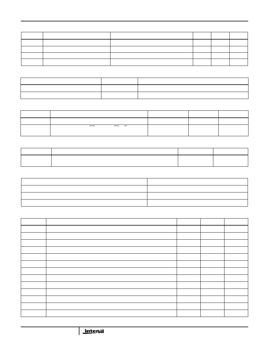
SDA vs SCL Timing
WP, A0, A1, and A2 Pin Timing
t
BUF
(Note 5)
Bus Free Time (Prior to Any Transmission)
1200
ns
t
SU:WPA
(Note 5)
A0, A1, A2 and WP Setup Time
600
ns
t
HD:WPA
(Note 5)
A0, A1, A2 and WP Hold Time
600
ns
2-Wire Interface timing (s)
(Continued)
SYMBOL
PARAMETER
MIN
MAX
UNITS
t
SU:STO
t
DH
t
HIGH
t
SU:STA
t
HD:STA
t
HD:DAT
t
SU:DAT
SCL
SDA
(Input Timing)
SDA
(Output Timing)
t
F
t
LOW
t
BUF
t
AA
t
R
t
HD:WP
SCL
SDA IN
WP, A0, A1, or A2
t
SU:WP
Clk 1
START
STOP
Increment/Decrement Timing
SYMBOL
PARAMETER
MIN
TYP (Note 4)
MAX
UNITS
t
CI
CS to SCL Setup
600
ns
t
ID
(Note 5)
SCL HIGH to U/D, DS0 or DS1 change
600
ns
t
DI
(Note 5)
U/D, DS0 or DS1 to SCL setup
600
ns
t
IL
SCL LOW period
2.5
µs
t
IH
SCL HIGH period
2.5
µs
t
IC
SCL inactive to CS inactive (Nonvolatile Store Setup Time)
1
µs
t
CPHS
CS deselect time (STORE)
10
ms
t
CPHNS
(Note 5)
CS deselect time (NO STORE)
1
µs
t
IW
(Note 5)
SCL to R
W
change
100
500
µs
t
CYC
SCL cycle time
5
µs
t
R
, t
F
(Note 5) SCL input rise and fall time
500
µs
X9252

7
FN8167.1
September 14, 2005
Increment/Decrement Timing
NOTES:
1. Absolute linearity is utilized to determine actual wiper voltage versus expected voltage = [V(R
W(n)(actual)
)-V(R
W(n)(expected)
)]/MI
V(R
W(n)(expected)
) = n(V(R
H
)-V(R
L
))/255 + V(R
L
), with n from 0 to 255.
2. Relative linearity is a measure of the error in step size between taps = [V(R
W(n+1)
)-(V(R
W(n)
) + MI)]/MI, with n from 0 to 254
3. 1 Ml = Minimum Increment = [V(R
H
)-V(R
L
)]/255.
4. Typical values are for T
A
= 25∞C and nominal supply voltage.
5. This parameter is not 100% tested.
6. Ratiometric temperature coefficient = (V(R
W
)
T1(n)
-V(R
W
)
T2(n)
)/[V(R
W
)
T1(n)
(T1-T2)] x 10
6
, with T1 & T2 being 2 temperatures, and n from 0 to
255.
7. Measured with wiper at tap position 255, R
L
grounded, using test circuit.
8. t
WC
is the minimum cycle time to be allowed for any nonvolatile write by the user, unless Acknowledge Polling is used. It is the time from a valid
STOP condition at the end of a write sequence of a 2-wire interface write operation, or from the rising edge of CS of a valid "Store" operation of
the Up/Down interface, to the end of the self-timed internal nonvolatile write cycle.
9. The recommended power up sequence is to apply V
CC
/V
SS
first, then the potentiometer voltages. During power up, the data sheet parameters
for the DCP do not fully apply until t
D
after V
CC
reaches its final value. In order to prevent unwanted tap position changes, or an inadvertant
store, bring the CS pin high before or concurrently with the V
CC
pin on power up.
CS
SCL
U/D
R
W
t
CI
t
IL
t
IH
t
CYC
t
ID
t
DI
t
IW
MI
(3)
t
IC
t
CPHS
t
F
t
R
10%
90%
90%
t
CPHNS
DS0, DS1
High-Voltage Write Cycle Timing
SYMBOL
PARAMETER
TYP
MAX
UNITS
t
WC
(Notes 5, 8)
Non-volatile write cycle time
5
10
ms
XDCP Timing
SYMBOL
PARAMETER
MIN
MAX
UNITS
t
WRL
(Note 5) SCL rising edge to wiper code changed, wiper response time after instruction
issued (all load instructions)
5
20
µs
X9252
8
FN8167.1
September 14, 2005
Test Circuit
Equivalent Circuit
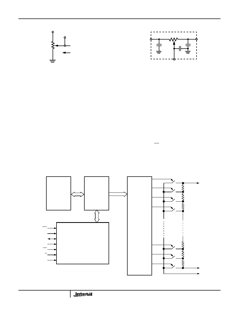
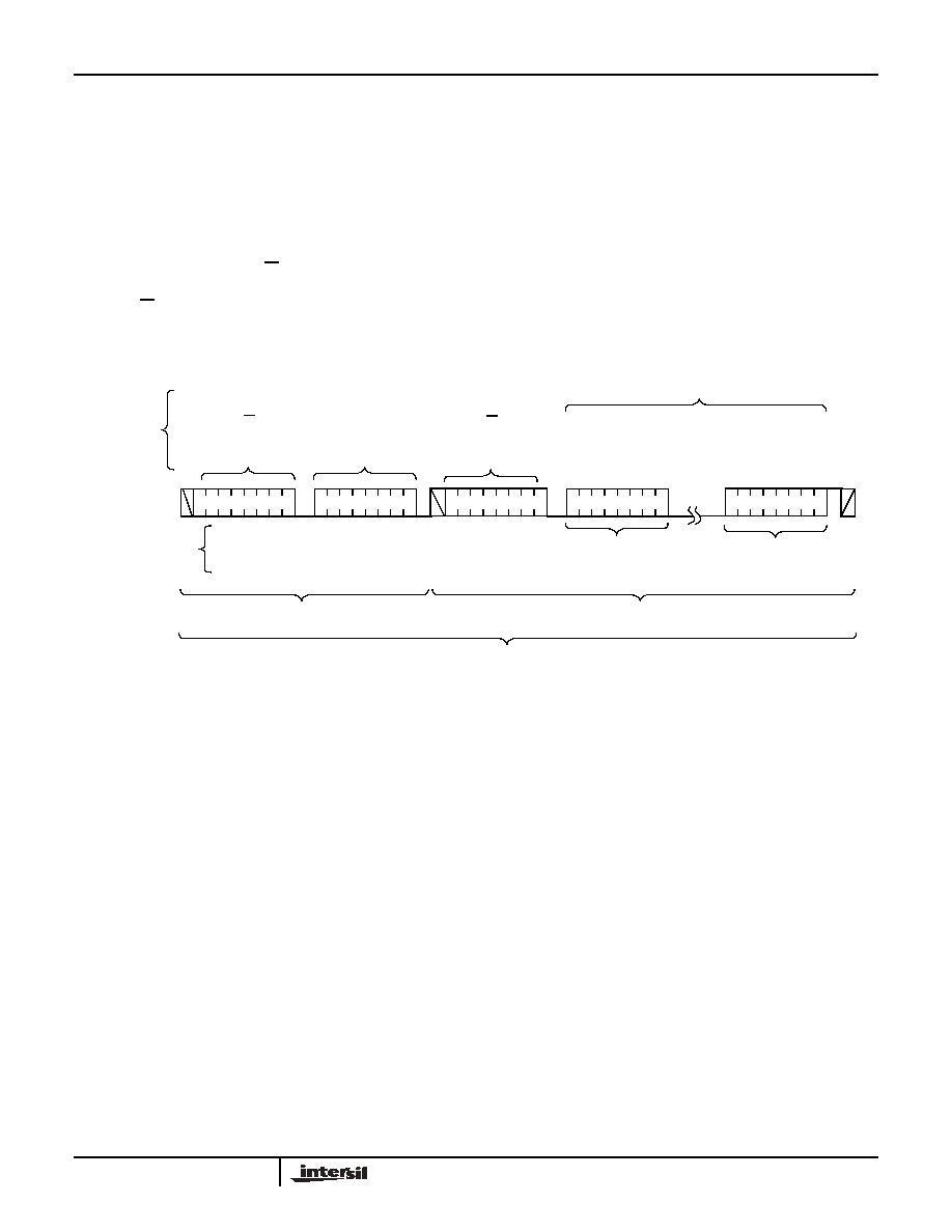
Principles of Operation
The X9252 is an integrated circuit incorporating four resistor
arrays, their associated registers and counters, and the
serial interface logic providing direct communication
between the host and the digitally controlled potentiometers.
This section provides detail description of the following:
- Resistor Array
- Up/Down Interface
- 2-wire Interface
Resistor Array Description
The X9252 is comprised of four resistor arrays. Each array
contains 255 discrete resistive segments that are connected
in series. The physical ends of each array are equivalent to
the fixed terminals of a mechanical potentiometer (R
Hi
and
R
Li
inputs) (See Figure 1.)
At both ends of each array and between each resistor
segment is a switch connected to the wiper (R
Wi
) pin.
Within each individual array only one switch may be turned
on at a time.
These switches are controlled by a Wiper Counter Register
(WCR). The 8-bits of the WCR (WCR[7:0]) are decoded to
select and enable one of 256 switches (see Table 1). Note
that each wiper has a dedicated WCR. When all bits of a
WCR are zeroes, the switch closest to the corresponding R
L
pin is selected. When all bits of a WCR are ones, the switch
closest to the corresponding R
H
pin is selected.
The WCR is volatile and may be written directly. There are
four non-volatile Data Registers (DR) associated with each
WCR. Each DR can be loaded into WCR. All DRs and
WCRs can be read or written.
Power Up and Down Requirements
During power up, CS must be high, to avoid inadvertant
"store" operations. At power up, the contents of Data
Registers DR00, DR10, DR20, and DR30, are loaded into
the corresponding wiper counter register.
Force
Current
Test Point
R
W
C
H
C
L
R
W
R
TOTAL
C
W
R
H
R
L
One
WCR[7:0]
R
Hi
R
Wi
R
Li
= FF hex
255
254
253
252
of
256
Decoder
Volatile
8-bit
Wiper
Counter
Register
WCRi
Four
Non-Volatile
Data
Registers
DRi0, DRi1,
DRi2, and
DRi3
i = 0, 1, 2, and 3
Interface Control and
WCR[7:0]
= 00 hex
2
1
0
Volatile Status Register (SR)
(Shared by the Four DCPs)
WP
SCL
SDA
A2, A1, A0
CS
U/D
DS1, DS0
FIGURE 1. DETAILED BLOCK DIAGRAM OF ONE DCP
X9252
9
FN8167.1
September 14, 2005
Up/Down Interface Operation
The SCL, U/D, CS, DS0 and DS1 inputs control the
movement of the wiper along the resistor array. With CS set
LOW the device is selected and enabled to respond to the
U/D and SCL inputs. HIGH to LOW transitions on SCL will
increment or decrement (depending on the state of the U/D
input) a wiper counter register selected by DS0 and DS1.
The output of this counter is decoded to select one of 256
wiper positions along the resistor array.
The value of the counter is stored in nonvolatile Data
Registers DRi0 whenever CS transitions HIGH while the
SCL and WP inputs are HIGH. "i" indicates the DCP number
selected with pins DS1 and DS0. During a "Store" operation
bits DRSel1 and DRSel0 in the Status Register must be both
"0", which is their power up default value. Other
combinations are reserved and must not be used.
The system may select the X9252, move the wiper, and
deselect the device without having to store the latest wiper
position in nonvolatile memory. After the wiper movement is
performed as described above and once the new position is
reached, the system must keep SCL LOW while taking CS
HIGH. The new wiper position will be maintained until
changed by the system or until a power-down/up cycle
recalled the previously stored data.
This procedure allows the system to always power-up to a
preset value stored in nonvolatile memory; then during
system operation minor adjustments could be made. The
adjustments might be based on user preference, system
parameter changes due to temperate drift, etc.
The state of U/D may be changed while CS remains LOW.
This allows the host system to enable the device and then
move the wiper up and down until the proper trim is attained.
The 2-wire interface is disabled while CS remains LOW.
Mode Selection for Up/Down Control
2-Wire Serial Interface
Protocol Overview
The device supports a bidirectional bus oriented protocol.
The protocol defines any device that sends data onto the
bus as a transmitter, and the receiving device as the
receiver. The device controlling the transfer is called the
master and the device being controlled is called the slave.
The master always initiates data transfers, and provides the
clock for both transmit and receive operations. The X9252
operates as a slave in all applications.
All 2-wire interface operations must begin with a START,
followed by a Slave Address byte. The Slave Address
selects the X9252, and specifies if a Read or Write operation
is to be performed.
All Communication over the 2-wire interface is conducted by
sending the MSB of each byte of data first.
Serial Clock and Data
Data states on the SDA line can change only while SCL is
LOW. SDA state changes while SCL is HIGH are reserved
for indicating START and STOP conditions (See Figure 2).
On power up of the X9252, the SDA pin is in the input mode.
Serial Start Condition
All commands are preceded by the START condition, which
is a HIGH to LOW transition of SDA while SCL is HIGH. The
device continuously monitors the SDA and SCL lines for the
START condition and does not respond to any command
until this condition has been met (See Figure 2).
Serial Stop Condition
All communications must be terminated by a STOP
condition, which is a LOW to HIGH transition of SDA while
SCL is HIGH. The STOP condition is also used to place the
device into the Standby power mode after a read sequence.
A STOP condition can only be issued after the transmitting
device has released the bus (See Figure 2).
TABLE 1. DCP SELECTION FOR UP/DOWN CONTROL
DS1
DS0
SELECTED DCP
0
0
DCP0
0
1
DCP1
1
0
DCP2
1
1
DCP3
CS
SCL
U/D
MODE
L
H
Wiper Up
L
L
Wiper Down
H
X
Store Wiper Position to nonvolatile
memory if WP pin is high. No store,
return to standby, if WP pin is low.
H
X
X
Standby
L
X
No Store, Return to Standby
L
H
Wiper Up (not recommended)
L
L
Wiper Down
(not recommended)
X9252

10
FN8167.1
September 14, 2005
Serial Acknowledge
An ACK (Acknowledge), is a software convention used to
indicate a successful data transfer. The transmitting device,
either master or slave, releases the bus after transmitting
eight bits. During the ninth clock cycle, the receiver pulls the
SDA line LOW to acknowledge the reception of the eight bits
of data (See Figure 3).
The device responds with an ACK after recognition of a
START condition followed by a valid Slave Address byte. A
valid Slave Address byte must contain the Device Type
Identifier 0101, and the Device Address bits matching the
logic state of pins A2, A1, and A0 (See Figure 4).
If a write operation is selected, the device responds with an
ACK after the receipt of each subsequent eight-bit word.
In the read mode, the device transmits eight bits of data,
releases the SDA line, and then monitors the line for an
ACK. The device continues transmitting data if an ACK is
detected. The device terminates further data transmissions if
an ACK is not detected. The master must then issue a STOP
condition to place the device into a known state.
Slave Address Byte
Following a START condition, the master must output a Slave
Address Byte (Refer to figure 4.). This byte includes three parts:
- The four MSBs (SA7-SA4) are the Device Type Identifier,
which must always be set to 0101 in order to select the
X9252.
- The next three bits (SA3-SA1) are the Device Address bits
(AS2-AS0). To access any part of the X9252's memory,
the value of bits AS2, AS1, and AS0 must correspond to
the logic levels at pins A2, A1, and A0 respectively.
- The LSB (SA0) is the R/W bit. This bit defines the
operation to be performed on the device being
addressed. When the R/W bit is "1", then a Read
operation is selected. A "0" selects a Write operation
.
SDA
SCL
START
DATA
DATA
STOP
STABLE
CHANGE
DATA
STABLE
FIGURE 2. VALID DATA CHANGES, START, AND STOP CONDITIONS
SDA Output from
Transmitter
SDA Output from
Receiver
8
1
9
START
ACK
SCL from Master
FIGURE 3. ACKNOWLEDGE RESPONSE FROM RECEIVER
SA6
SA7
SA5
SA3
SA2
SA1
SA0
Device Type
Identifier
Read or
SA4
SLAVE ADDRESS
BIT(S)
DESCRIPTION
SA7-SA4
Device Type Identifier
SA3-SA1
Device Address
SA0
Read or Write Operation Select
R/W
0
1
0
1
Address
Device
AS0
AS1
AS2
Write
FIGURE 4. SLAVE ADDRESS (SA) FORMAT
X9252
11
FN8167.1
September 14, 2005
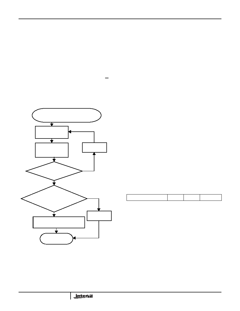
Nonvolatile Write Acknowledge Polling
After a nonvolatile write command sequence is correctly
issued (including the final STOP condition), the X9252
initiates an internal high voltage write cycle. This cycle
typically requires 5ms. During this time, any Read or Write
command is ignored by the X9252. Write Acknowledge
Polling is used to determine whether a high voltage write
cycle is completed.
During acknowledge polling, the master first issues a START
condition followed by a Slave Address Byte. The Slave
Address Byte contains the X9252's Device Type Identifier
and Device Address. The LSB of the Slave Address (R/W)
can be set to either 1 or 0 in this case. If the device is busy
within the high voltage cycle, then no ACK is returned. If the
high voltage cycle is completed, an ACK is returned and the
master can then proceed with a new Read or Write
operation. (Refer to figure 5.)
2-Wire Serial Interface Operation
X9252 Digital Potentiometer Register Organization
Refer to the Functional Diagram on page 2. There are four
Digitally Controlled Potentiometers, referred to as DCPi,
i=0,1,2,3. Each potentiometer has one volatile Wiper Control
Register (WCR) with the corresponding number, WCRi,
i=0,1,2,3. Each potentiometer also has four nonvolatile
registers to store wiper position or general data, these are
numbered DRi0, DRi1, DRi2 and DRi3, i=0,1,2,3.
The registers are organized in five pages of four, with one
page consisting of the WCRi (i=0-3), a second page
containing the DRi0 (i=0-3), a third page containing the
DRi1, and so forth. These pages can be written to four bytes
at time. In this manner all four potentiometer WCRs can be
updated in a single serial write (see "Page Write Operation"),
as well as all four registers of a given page in the DR array.
The unique feature of the X9252 device is that writing or
reading to a Data Register of a given DCP automatically
updates/moves the WCR of that DCP with the content of the
DR. In this manner data can be moved from a particular DCP
register to that DCP's WCR just by performing a 2-wire read
operation. Simultaneously, that data byte can be utilized by
the host.
Status Register Organization
The Status Register (SR) is used in read and write
operations to select the appropriate DCP register. Before
any DCP register can be accessed, the SR must be set to
the correct value. It is accessed by setting the Address Byte
to 07h (See Table 3). Do this by Writing the Slave Address
followed by a Byte Address of 07h. The SR is volatile and
defaults to 00h on power up. It is an 8-bit register containing
three control bits in the 3 LSBs as follows:
Bits DRSel1 and DRSel0 determine which Data Register of a
DCP is selected for a given operation. NVEnable is used to
select the volatile WCR if "0", and one of the nonvolatile
DCP registers if "1". Table 2 shows this register organization.
"Store" operations using the Up/Down interface require that
bits DRSel1 and DRSel0 are set to "0".
ACK returned?
Issue Slave Address
Byte (Read or Write)
Byte load completed by issuing
STOP. Enter ACK Polling
Issue STOP
Issue START
NO
YES
NO
Continue normal Read or Write
command sequence
PROCEED
YES
complete. Continue command
sequence.
High Voltage
Issue STOP
FIGURE 5. ACKNOWLEDGE POLLING SEQUENCE
7
6
5
4
3
2
1
0
Reserved
DRSel1
DRSel0
NVEnable
X9252
12
FN8167.1
September 14, 2005
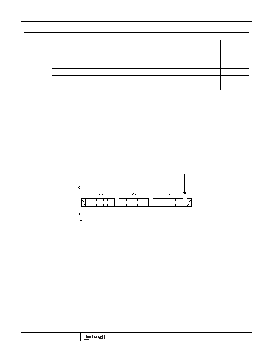
To read or write the contents of a single Data Register or Wiper Register:
1.
Load the status register (using a write command) to select the row (See Figure 6)
Writing a 1, 3, 5, or 7 to the Status Register specifies that the subsequent read or write command will access a Data Register. This Status
Register operation also initiates a transfer of the contents of the selected data register to its associated WCR for all DCPs. So, for example,
writing `03h' to the status register causes the value in DR01 to move to WCR0, DR11 to move to WCR1, DR21 to move to WCR2, and DR31
to move to WCR3.
Writing a 0 to bit `0' of the Status Register specifies that the subsequent read or write command will access a Wiper Counter Register. Each
WCR can be written to individually, without affecting the contents of any other.
2.
Access the desired DR or WCR using a new write or read command (see Figure 7 for write and Figure 9 for read.)
Specify the desired column (DCP number) by sending the DCP address as part of this read or write command.
TABLE 2. REGISTER NUMBERING
STATUS REG (Note 1) (Addr: 07H)
REGISTERED SELECTED (Note 2)
RESERVED
BITS 7-3
DRSel1
bit 2
DRSel0
bit 1
NVEnable
bit 0
DCP0
DCP1
DCP2
DCP3
(Addr: 00h)
(Addr: 01h)
(Addr: 02h)
(Addr: 03h)
Reserved
X
X
0
WCR0
WCR1
WCR2
WCR3
0
0
1
DR00
DR10
DR20
DR30
0
1
1
DR01
DR11
DR21
DR31
1
0
1
DR02
DR12
DR22
DR32
1
1
1
DR03
DR13
DR23
DR33
S
t
a
r
t
S
t
o
p
Slave
Address
Status Register
Address
Data
A
C
K
A
C
K
Signal at SDA
Signals from
the Slave
Signals from
the Master
0
A
C
K
If bit 0 of data byte = 1,
DR contents move to WCR
during this ACK period
0 1 0 1
0 0 0 0 0 1 1 1
0 0 0 0 0 x x 1
DR select
FIGURE 6. STATUS REGISTER WRITE (USES STANDARD BYTE WRITE SEQUENCE TO SET UP ACCESS TO A DATA REGISTER)
X9252
13
FN8167.1
September 14, 2005
DCP Addressing for 2-Wire Interface
Once the register number has been selected by a 2-wire
instruction, then the DCP number is determined by the
Address Byte of the following instruction. Note again that this
enables a complete page write of the DRs of all four
potentiometers at once. The register addresses accessible
in the X9252 include:
All other address bits in the Address Byte must be set to "0"
during 2-wire write operations and their value should be
ignored when read.
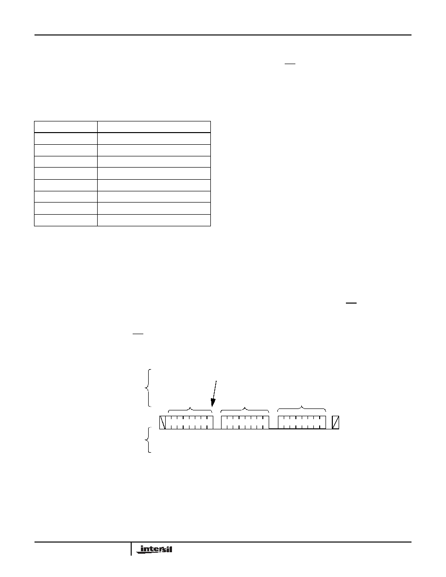
Byte Write Operation
For any Byte Write operation, the X9252 requires the Slave
Address byte, an Address Byte, and a Data Byte (See Figure
7). After each of them, the X9252 responds with an ACK.
The master then terminates the transfer by generating a
STOP condition. At this time, if the write operation is to a
volatile register (WCR, or SR), the X9252 is ready for the
next read or write operation. If the write operation is to a
nonvolatile register (DR), and the WP pin is high, the X9252
begins the internal write cycle to the nonvolatile memory.
During the internal nonvolatile write cycle, the X9252 does
not respond to any requests from the master. The SDA
output is at high impedance.
The SR bits and WP pin determine the register being
accessed through the 2-wire interface (See Table 2).
As noted before, any write operation to a Data Register
(DR), also transfers the contents of all the data registers in
that row to their corresponding WCR.
For example, to write 3Ahex to the Data Register 1 of DCP2
the following sequence is required:
During the sequence of this example, WP pin must be high,
and A0, A1, and A2 pins must be low. When completed, the
DR21 register and the WCR2 will be set to 3Ah and the other
Data Register in Row 1 will transfer their other contents to
the respective WCR's.
TABLE 3. 2-WIRE INTERFACE ADDRESS BYTE
ADDRESS (HEX)
CONTENTS
0
DCP 0
1
DCP 1
2
DCP 2
3
DCP 3
4
Not Used
5
Not Used
6
Not Used
7
Status Register
START
Slave Address
0101 0000
ACK
Address Byte
0000 0111
ACK
Data Byte
0000 0011
ACK
note: at this ACK, the WCRs are all updated with their respective DR.
STOP
START
Slave Address
0101 0000
ACK
Address Byte
0000 0010
ACK
Data Byte
0011 1010
ACK
STOP
(Hardware Address = 000,
and a Write command)
(Indicates Status Register
address)
(Data Register 1 and
NVEnable selected)
(Hardware address = 000,
(Access DCP2)
(Write Data Byte 3Ah)
Write command)
S
t
a
r
t
S
t
o
p
Slave
Address
Address
Byte
Data
Byte
A
C
K
Signals from the
Master
Signals from the
Slave
A
C
K
0
0
0
1
1
A
C
K
Write
Signal at SDA
FIGURE 7. BYTE WRITE SEQUENCE
X9252
14
FN8167.1
September 14, 2005
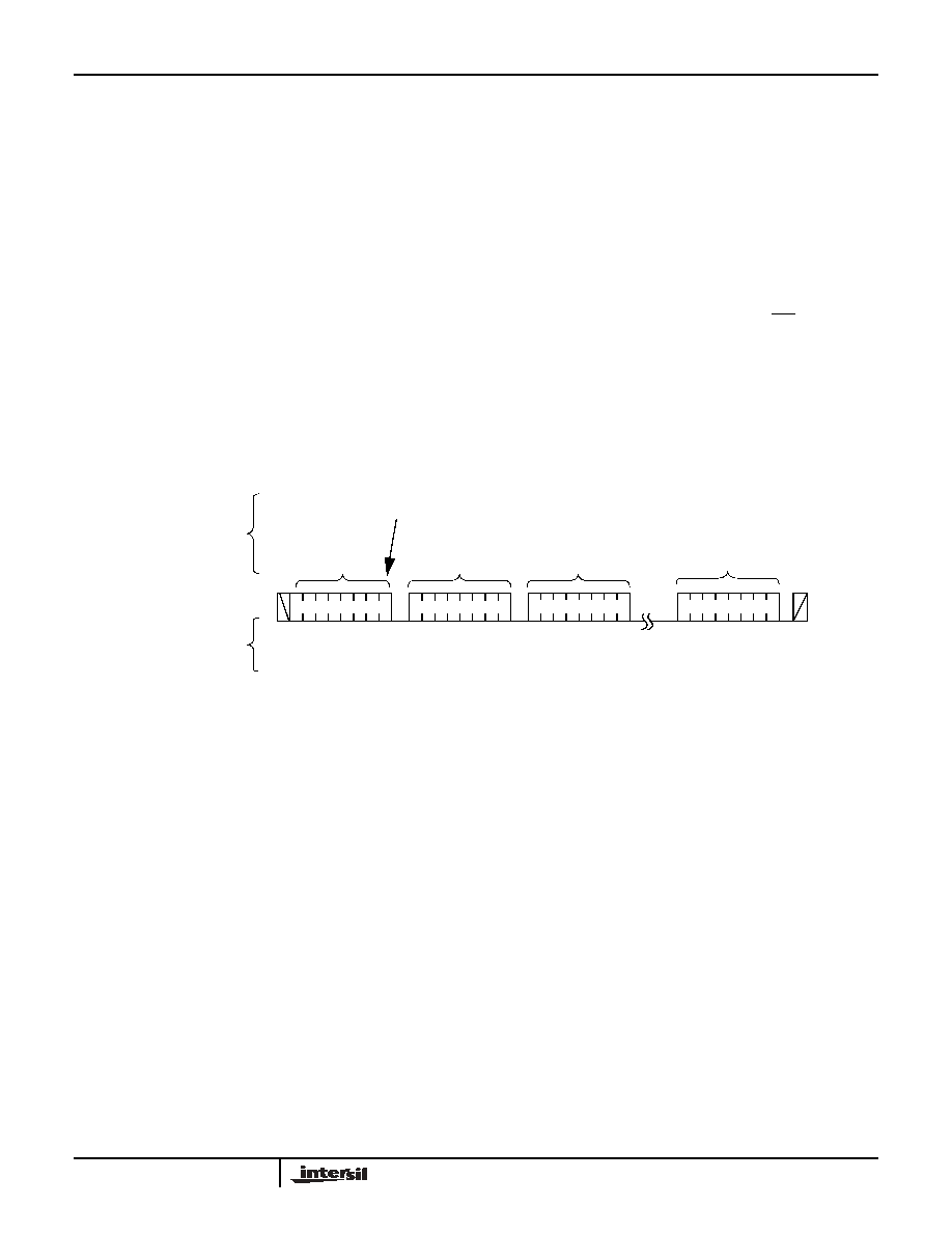
Page Write Operation
As stated previously, the memory is organized as a single
Status Register (SR), and four pages of four registers each.
Each page contains one Data Register for each DCP. The
order of the bytes within a page is DR0i, followed by DR1i,
followed by DR2i, and then DR3i, with i being the Data
Register number (0, 1, 2, or 3). Normally a page write
operation will be used to efficiently update all four data
registers and WCR in a single write command, starting at
DCP0 and finishing with DCP3.
In order to perform a Page Write operation to the memory
array, the NVEnable bit in the SR must first be set to "1".
A Page Write operation is initiated in the same manner as
the byte write operation; but instead of terminating the write
cycle after the first data byte is transferred, the master can
transmit up to 4 bytes (See Figure 8). After the receipt of
each byte, the X9252 responds with an ACK, and the
internal DCP address counter is incremented by one. The
page address remains constant. When the counter reaches
the end of the page (DR3i, 03hex), it "rolls over" and goes
back to the first byte of the same page (DR0i, 00hex).
For example, if the master writes 3 bytes to a page starting
at location DR22, the first 2 bytes are written to locations
DR22 and DR32, while the last byte is written to locations
DR02. Afterwards, the DCP counter would point to location
DR12. If the master supplies more than 4 bytes of data, then
new data overwrites the previous data, one byte at a time.
The master terminates the loading of Data Bytes by issuing
a STOP condition, which initiates the nonvolatile write cycle.
As with the Byte Write operation, all inputs are disabled until
completion of the internal write cycle. If the WP pin is low,
the nonvolatile write cycle doesn't start and the bytes are
discarded.
Notice that the Data Bytes are also written to the WCR of the
corresponding DCPs, therefore in the above example,
WCR2, WCR3, and WCR0 are also written and WCR1 is
updated with the contents of DR12.
2 < n < 4
Signals from the
Master
Signals from the
Slave
Signal at SDA
S
t
a
r
t
Slave
Address
Address
Byte
A
C
K
A
C
K
0
0
0
1
1
Data Byte (1)
S
t
o
p
A
C
K
A
C
K
Data Byte (n)
Write
FIGURE 8. PAGE WRITE OPERATION
X9252
15
FN8167.1
September 14, 2005
Move/Read Operation
The Move/Read operation simultaneously reads the
contents of a Data Register (DR) and moves the contents
into the corresponding DCP's WCR and the WCRs of all
DCPs are updated with the content of their corresponding
DR. Move/Read operation consists of a one byte, or three
byte instruction followed by one or more Data Bytes (See
Figure 9). To read an arbitrary byte, the master initiates the
operation issuing the following sequence: a START, the
Slave Address byte with the R/W bit set to "0", an Address
Byte, a second START, and a second Slave Address byte
with the R/W bit set to "1". After each of the three bytes, the
X9252 responds with an ACK. Then the X9252 transmits
Data Bytes as long as the master responds with an ACK
during the SCL cycle following the eight bit of each byte. The
master terminates the Move/Read operation (issuing a
STOP condition) following the last bit of the last Data Byte.
The first byte being read is determined by the current DCP
address and by the Status Register bits, according to Table
2. If more than one byte is read, the DCP address is
incremented by one after each byte, in the same way as
during a Page Write operation. After reaching DCP3, the
DCP address "rolls over" to DCP0.
On power up, the Address pointer is set to the Data Register
0 of DCP0.
Signals
from the
Master
Signals from the
Slave
Signal at SDA
S
t
a
r
t
Slave
Address with
R/W=0
Address
Byte
A
C
K
A
C
K
0
0
0
1
1
S
t
o
p
A
C
K
0
1
0
1
1
Slave
Address with
R/W=1
A
C
K
S
t
a
r
t
Last Read Data
Byte
First Read Data
Byte
A
C
K
One or more Data Bytes
Current Address Read
Setting the Current Address
Random Address Read
FIGURE 9. MOVE/READ SEQUENCE
X9252
16
FN8167.1
September 14, 2005
Applications Information
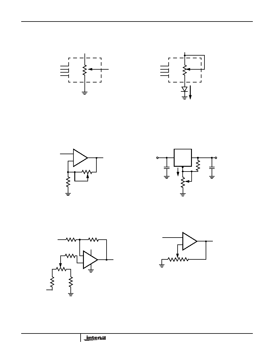
Basic Configurations of Electronic Potentiometers
Application Circuits
V
R
RW
+V
R
I
Three terminal
Potentiometer;
Variable voltage divider
Two terminal Variable
Resistor;
Variable current
NONINVERTING AMPLIFIER
VOLTAGE REGULATOR
OFFSET VOLTAGE ADJUSTMENT
COMPARATOR WITH HYSTERISIS
+
-
V
S
V
O
R
2
R
1
V
O
= (1+R
2
/R
1
)V
S
R
1
R
2
I
adj
V
O
(REG) = 1.25V (1+R
2
/R
1
)+I
adj
R
2
V
O
(REG)
V
IN
317
+
-
V
S
V
O
R
2
R
1
V
UL
= {R
1
/(R
1
+R
2
)} V
O
(max)
RL
L
= {R
1
/(R
1
+R
2
)} V
O
(min)
100k
10k
10k
10k
+5V
TL072
+
-
V
S
V
O
R
2
R
1
}
}
+5V
X9252
17
FN8167.1
September 14, 2005
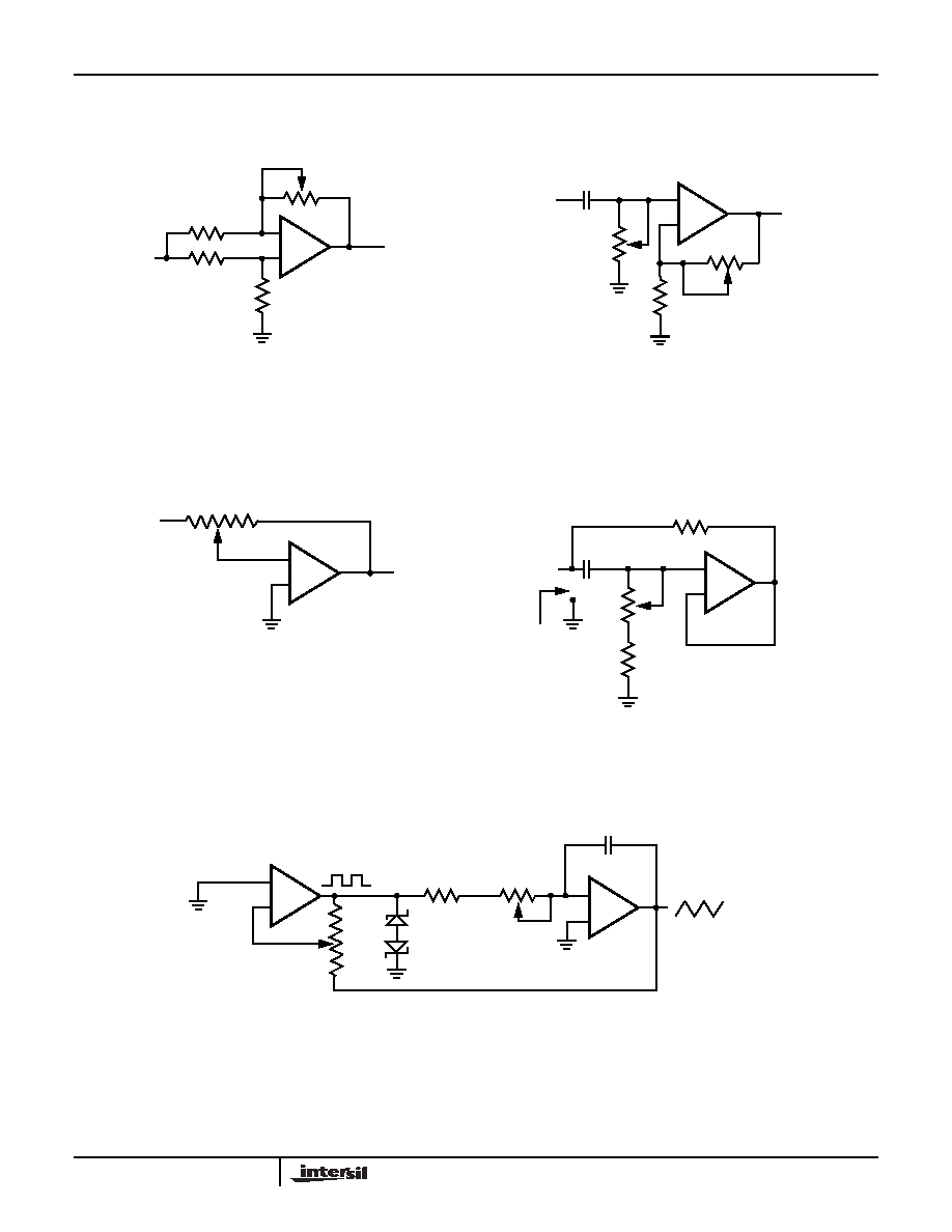
Application Circuits (Continued)
ATTENUATOR
FILTER
INVERTING AMPLIFIER
EQUIVALENT L-R CIRCUIT
+
-
V
S
V
O
R
3
R
1
V
O
= G V
S
-1/2
G +1/2
G
O
= 1 + R
2
/R
1
fc = 1/(2
RC)
+
-
V
S
V
O
R
2
R
1
Z
IN
= R
2
+ s R
2
(R
1
+ R
3
) C
1
= R
2
+ s Leq
(R
1
+ R
3
) >> R
2
+
-
V
S
FUNCTION GENERATOR
R
2
R
4
R
1
= R
2
= R
3
= R
4
= 10k
+
-
V
S
R
2
R
1
R
C
}
}
V
O
= G V
S
G = - R
2
/R
1
R
2
C
1
R
1
R
3
Z
IN
+
-
R
2
+
-
R
1
}
}
R
A
R
B
frequency
R
1
, R
2
, C
amplitude
R
A
, R
B
C
V
O
X9252
18
FN8167.1
September 14, 2005
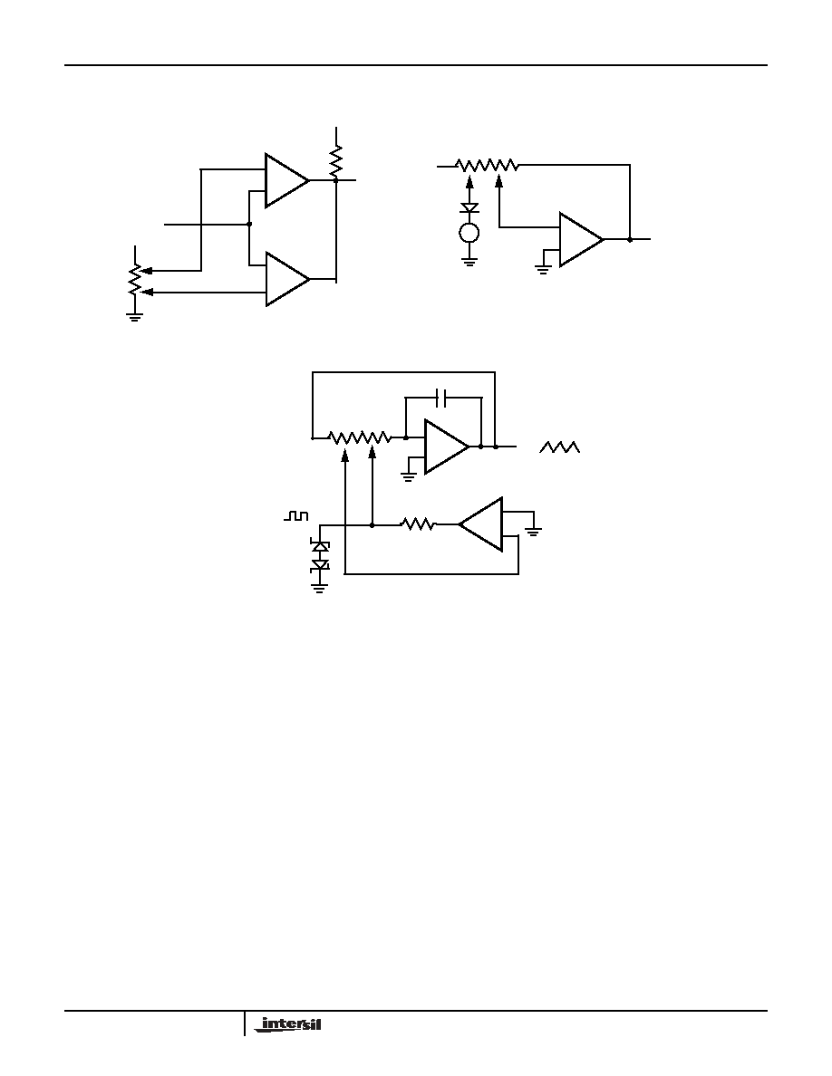
Application Circuits (Continued)
WINDOW COMPARATOR
SHUNT LIMITER
FUNCTION GENERATOR
+
-
V
S
V
O
V+
+
-
V
UL
V
LL
V+
+
-
V
S
V
O
}
}
V
R
+
}
mR nR pR
+
-
V
O
}
}
}
mR nR pR
C
+
-
X9252
19
All Intersil U.S. products are manufactured, assembled and tested utilizing ISO9000 quality systems.
Intersil Corporation's quality certifications can be viewed at www.intersil.com/design/quality
Intersil products are sold by description only. Intersil Corporation reserves the right to make changes in circuit design, software and/or specifications at any time without
notice. Accordingly, the reader is cautioned to verify that data sheets are current before placing orders. Information furnished by Intersil is believed to be accurate and
reliable. However, no responsibility is assumed by Intersil or its subsidiaries for its use; nor for any infringements of patents or other rights of third parties which may result
from its use. No license is granted by implication or otherwise under any patent or patent rights of Intersil or its subsidiaries.
For information regarding Intersil Corporation and its products, see www.intersil.com
FN8167.1
September 14, 2005
Packaging Information
NOTE: ALL DIMENSIONS IN INCHES (IN PARENTHESES IN MILLIMETERS)
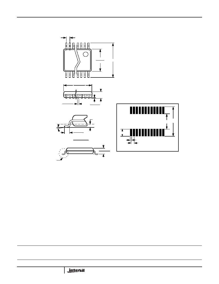
24-Lead Plastic, TSSOP, Package Code V24
.169 (4.3)
.177 (4.5)
.252 (6.4) BSC
.026 (.65) BSC
.303 (7.70)
.311 (7.90)
.002 (.06)
.005 (.15)
.047 (1.20)
.0075 (.19)
.0118 (.30)
See Detail "A"
.031 (.80)
.041 (1.05)
.010 (.25)
.020 (.50)
.030 (.75)
Gage Plane
Seating Plane
Detail A (20X)
(4.16) (7.72)
(1.78)
(0.42)
(0.65)
ALL MEASUREMENTS ARE TYPICAL
0∞-8∞
X9252